EP0408464A2 - Logische Operationseinheit für Bitfelder und ein diese enthaltender, monolithischer Mikroprozessor - Google Patents
Logische Operationseinheit für Bitfelder und ein diese enthaltender, monolithischer Mikroprozessor Download PDFInfo
- Publication number
- EP0408464A2 EP0408464A2 EP90402037A EP90402037A EP0408464A2 EP 0408464 A2 EP0408464 A2 EP 0408464A2 EP 90402037 A EP90402037 A EP 90402037A EP 90402037 A EP90402037 A EP 90402037A EP 0408464 A2 EP0408464 A2 EP 0408464A2
- Authority
- EP
- European Patent Office
- Prior art keywords
- logic operation
- bit
- mask pattern
- logic
- pattern generation
- Prior art date
- Legal status (The legal status is an assumption and is not a legal conclusion. Google has not performed a legal analysis and makes no representation as to the accuracy of the status listed.)
- Granted
Links
Images


Classifications
-
- G—PHYSICS
- G06—COMPUTING OR CALCULATING; COUNTING
- G06F—ELECTRIC DIGITAL DATA PROCESSING
- G06F7/00—Methods or arrangements for processing data by operating upon the order or content of the data handled
- G06F7/76—Arrangements for rearranging, permuting or selecting data according to predetermined rules, independently of the content of the data
- G06F7/764—Masking
-
- G—PHYSICS
- G06—COMPUTING OR CALCULATING; COUNTING
- G06F—ELECTRIC DIGITAL DATA PROCESSING
- G06F9/00—Arrangements for program control, e.g. control units
- G06F9/06—Arrangements for program control, e.g. control units using stored programs, i.e. using an internal store of processing equipment to receive or retain programs
- G06F9/30—Arrangements for executing machine instructions, e.g. instruction decode
- G06F9/30003—Arrangements for executing specific machine instructions
- G06F9/30007—Arrangements for executing specific machine instructions to perform operations on data operands
- G06F9/30018—Bit or string instructions
-
- G—PHYSICS
- G06—COMPUTING OR CALCULATING; COUNTING
- G06F—ELECTRIC DIGITAL DATA PROCESSING
- G06F9/00—Arrangements for program control, e.g. control units
- G06F9/06—Arrangements for program control, e.g. control units using stored programs, i.e. using an internal store of processing equipment to receive or retain programs
- G06F9/30—Arrangements for executing machine instructions, e.g. instruction decode
- G06F9/30003—Arrangements for executing specific machine instructions
- G06F9/30007—Arrangements for executing specific machine instructions to perform operations on data operands
- G06F9/30029—Logical and Boolean instructions, e.g. XOR, NOT
-
- G—PHYSICS
- G06—COMPUTING OR CALCULATING; COUNTING
- G06F—ELECTRIC DIGITAL DATA PROCESSING
- G06F9/00—Arrangements for program control, e.g. control units
- G06F9/06—Arrangements for program control, e.g. control units using stored programs, i.e. using an internal store of processing equipment to receive or retain programs
- G06F9/30—Arrangements for executing machine instructions, e.g. instruction decode
- G06F9/30003—Arrangements for executing specific machine instructions
- G06F9/30007—Arrangements for executing specific machine instructions to perform operations on data operands
- G06F9/30036—Instructions to perform operations on packed data, e.g. vector, tile or matrix operations
- G06F9/30038—Instructions to perform operations on packed data, e.g. vector, tile or matrix operations using a mask
Definitions
- This invention relates to a logic operation unit (LU) adapted for use in a computer system, more particularly, a bit field logic operation unit which performs a logic operation accompanied by a masking operation of a part of an operand.
- LU logic operation unit
- a logic operation such as AND, OR, EOR and the like accompanied by a masking operation is sometimes required.
- a bit or bits to be masked are specified by mask information,
- a bit or bits of an operand in the specified bit position are not altered by the logic operation, and only a remaining bit or bits are altered by the logic operation.
- This kind of operation can be performed by carrying out the following three processes:
- the logic operation accompanied by the mark operation is realized by controlling an ALU (Arithmetic Logic Unit) provided in the computer system according to a microprogram which is constituted from three microinstructions which correspond to these three processes 1) to 3), respectively.
- ALU Arimetic Logic Unit
- An object of the present invention is to provide a bit field logic operation unit which can perform a logic operation accompanied by a mask operation, within one machine cycle.
- Another object of the present invention is to provide the aforementioned bit field logic operation unit, wherein the unit is constituted from a small number of elements and the power consumption thereof is small.
- Still another object of the present invention is to provide a monolithic microprocessor wherein a bit manipulation instruction can be quickly executed, in particular, to provide a monolithic microprocessor wherein a variable-length bit field manipulation instruction, for example, an instruction to perform a specified logic operation on variable-length bit fields of a source data and a destination data and to store the operation result into a bit field of the destination side, can be executed within a smaller number of machine cycles.
- a bit manipulation instruction can be quickly executed
- a variable-length bit field manipulation instruction for example, an instruction to perform a specified logic operation on variable-length bit fields of a source data and a destination data and to store the operation result into a bit field of the destination side
- a bit field logic operation unit comprising a logic operation means for performing a specified logic operation on source data and destination data to output a logic operation result, a mask pattern generation means for simultaneously calculating a bit mask pattern from mask information in parallel with the operation of the logic operation means, and a bit map operation means for selecting either the logic operation result or the destination data in each bit position according to the bit mask pattern to output a masked logic operation result.
- the logic operation means and the mask pattern generation means are constituted by dynamic circuit constructions where the processes are performed in a precharge period to charge circuit elements according to input signals, and an active period to output processed data.
- precharge period of the logic operation means and the precharge period of the mask pattern generation means are carried out simultaneously.
- a monolithic microprocessor comprising an instruction receiving means for receiving an instruction, a control means for generating control signals according to the instruction transferred from the instruction receiving means, an arithmetic logic unit for performing an arithmetic logic operation in response to the control signal, and a bit field logic operation unit connected to the control means and for performing a logic operation on bit fields of parts of a source data and a destination data both of which comprise a plurality of bits, in response to a bit manipulation instruction, wherein the bit field logic operation unit comprise a logic operation means for performing a specified logic operation on source data and destination data to output a logic operation result, a mask pattern generation means for simultaneously generating a bit mask pattern from mask information in parallel with the operation of the logic operation means, and a bit map operation means for selecting either the logic operation result or the destination data in each bit position according to the bit mask pattern to output a masked logic operation result.
- Figure 1 shows a construction of an example of monolithic microprocessor, formed in a single semiconductor body comprising a logic operation unit according to the present invention.
- An instruction prefetching part 10 sends an instruction address to an address translation part 12 and issues an instruction prefetch request to the address translation part 12.
- the address translation part 12 translates the logical address into a physical address and transfers the translated address to an I/O control part 14.
- the I/O control part 14 prefetches an instruction and transfers it to the instruction prefetching part 10.
- the instruction prefetching part 10 transfers the prefetched instruction to an instruction decoding part 16.
- the instruction decoding part 16 decodes the instruction and transfers decoded information such as an origin address of microinstructions to an operation control part 18.
- the operation control part 18 sequentially reads out microinstructions from a microinstruction ROM 20 based on the origin address of microinstructions, stores each microinstruction into a microinstruction register 22, and controls an instruction executing part 24 according to the stored microinstruction and other decoded information to execute the instruction.
- the instruction executing part 24 comprises various types of operation units such as an ALU (Arithmetic Logic Unit) 26, a logic operation unit 28, and a register group 30.
- the operation units and the register groups 30 can exchange data with each other through buses 32, 34, and 36.
- a bit manipulation instruction, a variable-length bit field manipulation instruction, or the like is transferred from the instruction decoding part 16 to the operation control part 18.
- the operation control part 18 supplies the bit field logic operation unit 28 with a control signal, mask data D, and mask data input size M, and the instruction is executed in the bit field logic operation unit 28. As mentioned later, in this embodiment, these bit manipulations can be executed within one machine cycle.
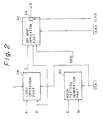
- Figure 2 shows a construction of the bit field logic operation unit 28 shown in Fig. 1.
- the bit field logic operation unit comprises a bit field logic operation part 38, a mask pattern generation part 40, and a bit map operation part 42.
- Source data A, destination data B and function signals F are supplied to the logic operation part 38, and a logic operation specified by the function signals is carried out on the source data A and the destination data B.
- Resulting logic values E from the operation in the logic operation unit 38 are supplied to the bit map operation part 42.
- Mask data D and a mask data input size M are supplied to the mask pattern generation part 40, and a mask pattern MPG is generated in the mask pattern generation part 40.
- the mask data D are, for example, information for specifying a bit position a more or less significant bit or bits of which are masked.
- the mask data input size M is, for example, information for specifying data type such as a byte or word.
- the destination data B, the logic values E and the mask pattern MPG are supplied to the bit map operation part 42.
- each bit of either E or B is selected according to the mask pattern MPG to form output data S.
- All of the logic operation part 38, the mask pattern generation part 40 and the bit map operation part 42 are constituted in a dynamic circuit construction where the operation is carried out in a precharge or preset period and an active period under control of a clock signal.
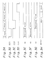
- Figures 3A to 3H are timing charts showing an operation of the bit field logic operation unit shown in Fig. 2.
- Fig. 3A represents four phases which constitute a machine cycle.
- Figs. 3B to 3D show waveforms of the CLK1 , CLK2 , and CLK0, respectively, shown in Fig. 2.
- Fig. 3E, Fig. 3F, and Fig. 3G represent operation modes of the logic operation part 38, the mask pattern generation part 40, and the bit map operation part 42.
- Fig. 3H represents a state of the output signal S.
- both the logic operation part 38 and the mask pattern generation part 40 are in the preset period, as the CLK1 supplied to both parts is at "low" level (Fig. 3B) in phase 1.
- Potentials of circuit nodes in the logic operation part 38 are preset and potentials of circuit nodes in the mask pattern generation part 40 are preset at the same time.
- both the logic operation part 38 and the mask pattern generation part 40 are in the active period, as the CLK1 is at "high” level.
- the logic operation part 38 outputs E according to the input A, B and F
- the mask pattern generation part 40 outputs MPG according to the input D and M.
- the bit map operation part 42 is in the preset period, as the CLK2 is at "low” level in phase 2. Therefore, potentials of circuit nodes in the bit map operation part 42 are preset.
- bit map operation part 42 is in the active period, as the CLK2 is at "high" level. There onlyfore the operation result is fixed within the bit map operation part 42 according to the E, MPG and B.
- phase 4 the output of the latch circuit 44 (Fig. 2) comprised in the bit map operation part 42 is valid as the CLK0 is at "high” level, so that the latch circuit 44 outputs the output signal S.
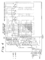
- Figure 4 shows a detailed construction of the mask pattern generation part 40.
- the mask data input size M represents a data type as shown in Table I.
- Table I M1 M0 data type MPG0-MPG7 MPG8-MPG15 MPG16-MPG23 MPG24-MPG31 0 0 byte x 1 1 1 0 1 half byte x x 1 1 1 0 word x x x x 1: all 1 X: determined by D
- MPG8 - MPG31 the upper 24 bits of MPG (MPG8 - MPG31) are forced to be "1" and the lower 8 bits of MPG are determined by the mask data D.
- the mask data D specifies a bit position which defines the most significant bit of bits having value of "0" as shown in Table II.
- Figure 5 shows detailed constructions of the logic operation part 38 and the bit map operation part 42.
- the least significant bits A0 , B0 , MPG0 , and S0
- Portions for other bits A1 ⁇ 31 , B1 ⁇ 31 , MPG1 ⁇ 31 , and S1 ⁇ 31 are identical.
- the logic operation part 38 performs a logic operation specified by the F0 to F3 on the source data A and the destination data B, and outputs E, as shown in Table III.
- Table III F3 F2 F1 F0 E 0 0 0 0 0 0 0 0 1 B AND A 0 0 1 1 A 0 1 0 0 B AND A 0 1 0 1 B 0 1 1 0 B XOR A 0 1 1 1 B OR A 1 0 0 0 B AND A 1 0 0 1 B XOR A 1 0 1 0 B 1 0 1 1 B OR A 1 1 0 0 0 A 1 1 0 1 B OR A 1 1 1 1 0 1 0 1 B OR A 1 1 1 0 0 B OR A 1 1 1 1 0 B OR A 1 1 1 1 0 B OR A 1 1 1 1 0 B OR A 1 1 1 1 0 B OR A 1 1 1 1 0 B OR A 1 1 1 1 1 1 1 1 1 1 1 1 B OR A 1
- Figure 6 shows another embodiment of the bit map operation part 42.
- the signals U, L and N are signals for specifying a masking mode.
- a bit or bits of output signal S corresponding to a bit or bits of MPG having a logic value "1” become corresponding bit or bits of E
- a bit or bits of output signal S corresponding to a bit or bits of MPG having a logic value "0” become corresponding bit or bits of B, namely, the upper bit or bits are unmasked.
- the signal L is "1”
- a lower bit or bits are unmasked.
- the signal N is "1" all bits are unmasked.
Landscapes
- Engineering & Computer Science (AREA)
- Theoretical Computer Science (AREA)
- Software Systems (AREA)
- Physics & Mathematics (AREA)
- General Engineering & Computer Science (AREA)
- General Physics & Mathematics (AREA)
- Mathematical Physics (AREA)
- Executing Machine-Instructions (AREA)
- Image Processing (AREA)
Applications Claiming Priority (2)
| Application Number | Priority Date | Filing Date | Title |
|---|---|---|---|
| JP178930/89 | 1989-07-13 | ||
| JP17893089 | 1989-07-13 |
Publications (3)
| Publication Number | Publication Date |
|---|---|
| EP0408464A2 true EP0408464A2 (de) | 1991-01-16 |
| EP0408464A3 EP0408464A3 (en) | 1992-08-19 |
| EP0408464B1 EP0408464B1 (de) | 1996-09-18 |
Family
ID=16057128
Family Applications (1)
| Application Number | Title | Priority Date | Filing Date |
|---|---|---|---|
| EP90402037A Expired - Lifetime EP0408464B1 (de) | 1989-07-13 | 1990-07-13 | Logische Operationseinheit für Bitfelder und ein diese enthaltender, monolithischer Mikroprozessor |
Country Status (5)
| Country | Link |
|---|---|
| US (1) | US5457803A (de) |
| EP (1) | EP0408464B1 (de) |
| JP (1) | JP2567134B2 (de) |
| KR (1) | KR930009632B1 (de) |
| DE (1) | DE69028583D1 (de) |
Cited By (1)
| Publication number | Priority date | Publication date | Assignee | Title |
|---|---|---|---|---|
| EP0454636A1 (de) * | 1990-04-26 | 1991-10-30 | STMicroelectronics S.r.l. | Verfahren zur Durchführung boolescher Operationen zwischen zwei beliebige Bits von zwei beliebigen Registern |
Families Citing this family (4)
| Publication number | Priority date | Publication date | Assignee | Title |
|---|---|---|---|---|
| JP3433588B2 (ja) * | 1995-10-19 | 2003-08-04 | 株式会社デンソー | マスクデータ生成回路及びビットフィールド操作回路 |
| JP3560596B2 (ja) | 2002-08-22 | 2004-09-02 | 沖電気工業株式会社 | 演算装置及びデータの読出方法 |
| CN104011650B (zh) | 2011-12-23 | 2017-09-19 | 英特尔公司 | 使用输入写掩码和立即数从源写掩码寄存器在目的地写掩码寄存器中设置输出掩码的系统、装置和方法 |
| KR102075260B1 (ko) | 2018-08-07 | 2020-02-07 | 김윤식 | 마늘 분쇄기 |
Family Cites Families (4)
| Publication number | Priority date | Publication date | Assignee | Title |
|---|---|---|---|---|
| US4400794A (en) * | 1981-11-17 | 1983-08-23 | Burroughs Corporation | Memory mapping unit |
| US4785393A (en) * | 1984-07-09 | 1988-11-15 | Advanced Micro Devices, Inc. | 32-Bit extended function arithmetic-logic unit on a single chip |
| JPS61262923A (ja) * | 1985-05-17 | 1986-11-20 | Sharp Corp | パイプライン方式デ−タ処理回路の先まわり制御回路 |
| JP2583525B2 (ja) * | 1987-09-30 | 1997-02-19 | 健 坂村 | データ処理装置 |
-
1990
- 1990-07-13 JP JP2184088A patent/JP2567134B2/ja not_active Expired - Fee Related
- 1990-07-13 EP EP90402037A patent/EP0408464B1/de not_active Expired - Lifetime
- 1990-07-13 KR KR1019900010655A patent/KR930009632B1/ko not_active Expired - Fee Related
- 1990-07-13 DE DE69028583T patent/DE69028583D1/de not_active Expired - Lifetime
-
1994
- 1994-02-28 US US08/202,876 patent/US5457803A/en not_active Expired - Fee Related
Cited By (1)
| Publication number | Priority date | Publication date | Assignee | Title |
|---|---|---|---|---|
| EP0454636A1 (de) * | 1990-04-26 | 1991-10-30 | STMicroelectronics S.r.l. | Verfahren zur Durchführung boolescher Operationen zwischen zwei beliebige Bits von zwei beliebigen Registern |
Also Published As
| Publication number | Publication date |
|---|---|
| EP0408464A3 (en) | 1992-08-19 |
| JPH03129425A (ja) | 1991-06-03 |
| US5457803A (en) | 1995-10-10 |
| DE69028583D1 (de) | 1996-10-24 |
| JP2567134B2 (ja) | 1996-12-25 |
| KR910003941A (ko) | 1991-02-28 |
| KR930009632B1 (ko) | 1993-10-08 |
| EP0408464B1 (de) | 1996-09-18 |
Similar Documents
| Publication | Publication Date | Title |
|---|---|---|
| KR100266337B1 (ko) | 정보처리회로,반도체집적회로장치,마이크로컴퓨터,및전자기기 | |
| KR100440841B1 (ko) | 마이크로컴퓨터 | |
| US6446190B1 (en) | Register file indexing methods and apparatus for providing indirect control of register addressing in a VLIW processor | |
| US4037213A (en) | Data processor using a four section instruction format for control of multi-operation functions by a single instruction | |
| US7350054B2 (en) | Processor having array of processing elements whose individual operations and mutual connections are variable | |
| JP3954171B2 (ja) | コンピュータにおけるスカラ値をベクトルに記入する方法 | |
| WO2004053718A1 (en) | Cellular engine for a data processing system | |
| JP2001142697A (ja) | データ処理装置 | |
| JP2622612B2 (ja) | 集積回路 | |
| JPH0470662B2 (de) | ||
| US5666510A (en) | Data processing device having an expandable address space | |
| EP1680735B1 (de) | Vorrichtung und verfahren zur ermöglichung mehrerer anweisungssätze und mehrerer decodierungsbetriebsarten | |
| US5757685A (en) | Data processing system capable of processing long word data | |
| GB2092786A (en) | Stored-program controlled machine | |
| US5687344A (en) | Single-chip microcomputer having an expandable address area | |
| JPH11272546A (ja) | 可変長レジスタ装置 | |
| EP0614137B1 (de) | Datenverarbeitungssystem und -Verfahren mit einem erweitbaren Register | |
| EP0408464A2 (de) | Logische Operationseinheit für Bitfelder und ein diese enthaltender, monolithischer Mikroprozessor | |
| US5363322A (en) | Data processor with an integer multiplication function on a fractional multiplier | |
| US5077659A (en) | Data processor employing the same microprograms for data having different bit lengths | |
| US6975250B2 (en) | Methods and systems for data manipulation | |
| JPH034936B2 (de) | ||
| JP3727395B2 (ja) | マイクロコンピュータ | |
| JPH0685147B2 (ja) | 半導体回路装置 | |
| US5708800A (en) | High speed microprocessor for processing and transferring N-bits of M-bit data |
Legal Events
| Date | Code | Title | Description |
|---|---|---|---|
| PUAI | Public reference made under article 153(3) epc to a published international application that has entered the european phase |
Free format text: ORIGINAL CODE: 0009012 |
|
| AK | Designated contracting states |
Kind code of ref document: A2 Designated state(s): DE FR GB |
|
| PUAL | Search report despatched |
Free format text: ORIGINAL CODE: 0009013 |
|
| AK | Designated contracting states |
Kind code of ref document: A3 Designated state(s): DE FR GB |
|
| 17P | Request for examination filed |
Effective date: 19930127 |
|
| 17Q | First examination report despatched |
Effective date: 19951004 |
|
| GRAH | Despatch of communication of intention to grant a patent |
Free format text: ORIGINAL CODE: EPIDOS IGRA |
|
| GRAH | Despatch of communication of intention to grant a patent |
Free format text: ORIGINAL CODE: EPIDOS IGRA |
|
| GRAA | (expected) grant |
Free format text: ORIGINAL CODE: 0009210 |
|
| AK | Designated contracting states |
Kind code of ref document: B1 Designated state(s): DE FR GB |
|
| PG25 | Lapsed in a contracting state [announced via postgrant information from national office to epo] |
Ref country code: FR Effective date: 19960918 |
|
| REF | Corresponds to: |
Ref document number: 69028583 Country of ref document: DE Date of ref document: 19961024 |
|
| PG25 | Lapsed in a contracting state [announced via postgrant information from national office to epo] |
Ref country code: DE Effective date: 19961219 |
|
| EN | Fr: translation not filed | ||
| PLBE | No opposition filed within time limit |
Free format text: ORIGINAL CODE: 0009261 |
|
| STAA | Information on the status of an ep patent application or granted ep patent |
Free format text: STATUS: NO OPPOSITION FILED WITHIN TIME LIMIT |
|
| 26N | No opposition filed | ||
| REG | Reference to a national code |
Ref country code: GB Ref legal event code: IF02 |
|
| PGFP | Annual fee paid to national office [announced via postgrant information from national office to epo] |
Ref country code: GB Payment date: 20060712 Year of fee payment: 17 |
|
| GBPC | Gb: european patent ceased through non-payment of renewal fee |
Effective date: 20070713 |
|
| PG25 | Lapsed in a contracting state [announced via postgrant information from national office to epo] |
Ref country code: GB Free format text: LAPSE BECAUSE OF NON-PAYMENT OF DUE FEES Effective date: 20070713 |