EP0409245A2 - Mit verbesserter Ausgangsstruktur ausgestattetes Ladungstransfer-Bauelement - Google Patents
Mit verbesserter Ausgangsstruktur ausgestattetes Ladungstransfer-Bauelement Download PDFInfo
- Publication number
- EP0409245A2 EP0409245A2 EP90113876A EP90113876A EP0409245A2 EP 0409245 A2 EP0409245 A2 EP 0409245A2 EP 90113876 A EP90113876 A EP 90113876A EP 90113876 A EP90113876 A EP 90113876A EP 0409245 A2 EP0409245 A2 EP 0409245A2
- Authority
- EP
- European Patent Office
- Prior art keywords
- reset
- gate electrode
- drain region
- charge transfer
- region
- Prior art date
- Legal status (The legal status is an assumption and is not a legal conclusion. Google has not performed a legal analysis and makes no representation as to the accuracy of the status listed.)
- Granted
Links
- 230000004888 barrier function Effects 0.000 claims abstract description 32
- 239000000758 substrate Substances 0.000 claims abstract description 17
- 238000010521 absorption reaction Methods 0.000 claims abstract description 15
- 239000004065 semiconductor Substances 0.000 claims abstract description 15
- 239000003990 capacitor Substances 0.000 claims abstract description 13
- 239000012535 impurity Substances 0.000 claims description 10
- XUIMIQQOPSSXEZ-UHFFFAOYSA-N Silicon Chemical compound [Si] XUIMIQQOPSSXEZ-UHFFFAOYSA-N 0.000 claims description 4
- 229910052710 silicon Inorganic materials 0.000 claims description 4
- 239000010703 silicon Substances 0.000 claims description 4
- 230000000694 effects Effects 0.000 description 3
- 230000006866 deterioration Effects 0.000 description 2
- 238000010586 diagram Methods 0.000 description 2
- 238000012986 modification Methods 0.000 description 2
- 230000004048 modification Effects 0.000 description 2
- 229910021420 polycrystalline silicon Inorganic materials 0.000 description 2
- 230000004075 alteration Effects 0.000 description 1
- 230000015572 biosynthetic process Effects 0.000 description 1
- 230000002708 enhancing effect Effects 0.000 description 1
- 230000005669 field effect Effects 0.000 description 1
- 230000002093 peripheral effect Effects 0.000 description 1
Images


Classifications
-
- G—PHYSICS
- G11—INFORMATION STORAGE
- G11C—STATIC STORES
- G11C27/00—Electric analogue stores, e.g. for storing instantaneous values
- G11C27/04—Shift registers
-
- G—PHYSICS
- G11—INFORMATION STORAGE
- G11C—STATIC STORES
- G11C19/00—Digital stores in which the information is moved stepwise, e.g. shift registers
- G11C19/28—Digital stores in which the information is moved stepwise, e.g. shift registers using semiconductor elements
- G11C19/282—Digital stores in which the information is moved stepwise, e.g. shift registers using semiconductor elements with charge storage in a depletion layer, i.e. charge coupled devices [CCD]
- G11C19/285—Peripheral circuits, e.g. for writing into the first stage; for reading-out of the last stage
-
- H—ELECTRICITY
- H10—SEMICONDUCTOR DEVICES; ELECTRIC SOLID-STATE DEVICES NOT OTHERWISE PROVIDED FOR
- H10D—INORGANIC ELECTRIC SEMICONDUCTOR DEVICES
- H10D44/00—Charge transfer devices
- H10D44/40—Charge-coupled devices [CCD]
- H10D44/45—Charge-coupled devices [CCD] having field effect produced by insulated gate electrodes
- H10D44/462—Buried-channel CCD
Definitions
- the present invention relates to a solid-state charge transfer device such as a charge coupled device (CCD).
- CCD charge coupled device
- a floating diffused region is widely used as charge detecting means in a solid-state charge transfer device.
- a signal charge transferred through the channel region of a charge transfer section is led to the floating diffused region.
- the charges are drained to a reset drain through a channel under a reset gate.
- the floating diffused region and the reset drain region are impurity-doped regions separately formed in a semiconductor substrate.
- the reset gate is provided on the semiconductor substrate between the floating diffused region and the reset drain region via an insulating layer.
- the floating diffused region, the reset gate electrode and the reset drain region constitute a field effect transistor (reset transistor).
- the drain of charges from the floating diffused region is achieved by turning this reset transistor on.
- the potential of the reset drain should be higher than a certain level and held at that certain level.
- the channel potential under the reset gate electrode in the aforementioned on-state of the reset transistor should be somewhat lower than that of the reset drain region.
- the amplitude of the reset pulse to be applied to the reset gate electrode is usually greater than that of the transfer pulse of the charge transfer section. For instance, in an n-type buried channel charge coupled device, the amplitude of the transfer pulse is 5 volts; that of the reset pulse, 8 volts, and the voltage supplied to the reset drain region, 12 volts.
- the channel potential under the reset gate electrode changes between 7 volts and approximately 13.5 volts.
- the channel potential (about 13.5 V) of a reset transistor in on-state is higher than the drain voltage, which is 12 volts, the reset transistor is driven into an on-state of a complete transfer mode to reset the potential of the floating diffused region to that of the reset drain region.
- the power voltage for the peripheral circuits using the output from the charge coupled device is as low as 5 volts, for instance, so that the charge coupled device operable at a low power voltage is widely demanded.
- the drain voltage of 12 volts can be realized with relative ease with a voltage booster.
- a voltage booster for enhancing 5 volts of the reset pulse to 8 volts is more complex to provide than the aforementioned voltage booster from 5 volts to 15 volts and accordingly should one of circuits to be avoided in a semiconductor integrated circuit.
- the channel potential of the reset transistor in on-state is about 11 volts in the above cited example, lower than the 12 volts in potential at the reset drain region.
- the reset transistor is driven into an on-state in an incomplete transfer mode. Under such incomplete transfer mode operation, it is impossible to completely drain the signal charges from the floating diffused region, and the dynamic range of the signal output will become correspondingly narrower.
- first and second gates are arranged between the floating diffused region and the reset drain region.
- the first gate similar to the charge transfer section, includes a pair of a barrier electrode and a storage electrode.
- the second gate is supplied with the same voltage as the output gate which is formed in adjacent to the floating diffused region in the charge transfer section, but the insulating film formed thereunder is thickened to keep the channel potential thereunder lower than the channel potential under the output gate.
- the charges in the floating diffused region, after being transferred to under the storage electrode of the first gate, are drained to the reset drain region.
- the first gate receives the same pulse as what is supplied to the output gate. In this way, the voltage supplied to the reset drain region can be lowered, because the potential at the reset drain region is sufficient to have a value slightly deeper than the channel potential under the storage electrode of the first gate when the channel potential takes a lower one.
- the transfer from the floating diffused region to under the storage electrode of the first gate is performed in an incomplete transfer mode, because the channel potential under the first barrier electrode is lower than that under the storage electrode.
- a third gate and an intermediate drain are arranged between the floating diffused region and the first gate in the first example, and a large-capacity capacitor is connected between the intermediate drain and the grounding terminal.
- the charges in the floating diffused region after being first drained into this intermediate drain through the third gate, are finally drained into the reset drain held at a constant voltage.
- the transfer of charges from the floating diffused region to the reset drain is performed in a complete transfer mode.
- the potential at the reset drain can be further lowered. A pulse of a greater amplitude is required, however, when the charge under the storage electrode of the first gate is drained into the reset drain.
- the potential at the reset drain in both the first and the second examples, is made lower than the channel potential under the storage electrode.
- An object of the present invention is to provide an electric charge transfer device capable of normal operation with a single low-voltage power source.
- Another object of the invention is to provide an electric charge transfer device free from the deterioration of the dynamic range even if the amplitude of the reset pulse is equal to that of the transfer pulse.
- an output gate is arranged as a final stage of a charge transfer section, and a floating diffused region is provided adjacent to the output gate.
- a reset gate electrode adjacent to the floating diffused region, and adjacent to the reset gate electrode is a reset drain region.
- a large-capacity capacitor is connected between the reset drain region and a reference potential terminal.
- a barrier gate adjoins the reset drain region, and an absorption drain region is arranged next to the barrier gate.
- the barrier gate has a barrier gate electrode, provided on a semiconductor substrate via a gate insulating film, and the channel potential under the barrier gate electrode is lower than that of the reset gate electrode when in resetting operation.
- the preferred state of the means is realized by somewhat elongating the gate length of the barrier gate electrode when a reset gate electrode has a proper gate length to be accompanied by a short channel effect.
- This voltage booster can be readily realized with a circuit to enlarge the amplitude of the transfer pulse supplied to the charge transfer section.
- the presence of the voltage booster makes it possible to sufficiently deepen the potential of the absorption drain region even if the voltage of the power source is low.
- the charges in the floating diffused region are periodically drained, first temporarily to the reset drain region connected to the capacitor and then to the absorption drain connected to the voltage booster. As the large-capacity capacitor is connected to the reset drain region, its potential fluctuations can be ignored.
- the potential at the reset drain region can be deemed to be fixed at the channel potential under the barrier gate electrode. As the potential under the barrier gate electrode is set shallower than that under the reset gate electrode, the reset transistor consisting of the floating diffused region, the reset gate electrode and the reset drain region is driven into an on-state of a complete transfer mode. Signal charges remaining in the floating diffused region can be completely drained with a low-voltage power source.
- an n-type diffused region 2 is formed over the surface of a p-type silicon substrate 1 whose impurity concentration is 5 x 1015 cm ⁇ 3.
- the impurity concentration, thickness and width of the n-type diffused region 2 are 2 x 1016 cm ⁇ 3, 1 micron meters and 10 micron meters, respectively.
- Over the surface of the silicon substrate 1 is provided a 100 nm thick gate oxide film 4, over which are arranged transfer electrodes 5a and 5b, an output gate electrode 6 and a reset gate electrode 8.
- These electrodes are made of phosphorus-doped polycrystalline silicon films of 400 nm in thickness and 20 ⁇ / in sheet resistance. Every one of them is 5 microns in width (gate length).
- n-type diffused region 2 (n-type buried channel) under the transfer electrodes are alternately formed p-type barrier regions 3 (1 x 1015 cm ⁇ 3 in impurity concentration and at most 0.1 micron meters in thickness).
- the transfer electrode provided with one of the p-type barrier layers 3 is the barrier electrode, while that provided with none is the storage electrode.
- An n+-type floating diffused region 7 (2 x 1017 cm ⁇ 3 in impurity concentration) is provided adjacent to a position immediately beneath the output gate electrode 6.
- the position immediately beneath the reset gate electrode 8 adjoins the floating diffused region 7 on one side and a reset drain 9 (an n+-type diffused region of 2 x 1017 cm ⁇ 3 in impurity concentration) on the other.
- transfer clocks ⁇ 1 and ⁇ 2 which are 5 V at the high level and 0 V at the low level and 180° apart in phase from each other.
- a fixed gate voltage V OG (3 V for example) is applied to the output gate electrode 6 to control the flow of charges from the charge transfer section into the floating diffused region 7.
- a reset clock ⁇ R which is the same as the clock ⁇ 1 in phase, but shorter than the clock ⁇ 1 in high level duration, 5 V at the high level and 0 V at the level, to reset the potential of the floating diffused region 7 to that of the reset drain region 9 at regular intervals by draining charges in the floating diffused region 7 to the reset drain region 9.
- the floating diffused region 7 is connected to the gate electrode of an enhancement type n channel MOS transistor Tr1 in a source follower circuit, which consists of the transistor Tr1 and a depression type n channel MOS transistor Tr2.
- the reset drain 9 is grounded via a capacitor C, whose capacity is 100 to 1,000 times as great as that of the capacity (for instance 0.01 pF) of the floating diffused region 7, 5 pF for example.
- a barrier gate electrode 10 (phosphorus-doped polycrystalline silicon film) of 10 micron meters in gate length is provided via the gate oxide film 4 over the n-type diffused region 2 adjoining the reset drain region 9, and connected to an external power source 16.
- MOS transistors M1, M2, ...., M8 are connected in cascade in the voltage booster 15. These MOS transistors have a common gate oxide film of 100 microns in the thickness and source/drain regions of 2 x 1017 cm ⁇ 3 in impurity concentration and present a threshold voltage of 0.7 volts.
- the MOS transistors M1 to M8 are formed on the same semiconductor chip as the n-type buried channel charge coupled device.
- the gate of the MOS transistor M1 is supplied with the transfer clock ⁇ 1.
- the transfer clock ⁇ 1 is also supplied to the output side of the MOS transistors M2, M4, M6 and M8 through capacitors C2, C4, C6 and C8.
- To the output side of the MOS transistors M1, M3, M5 and M7 is supplied the transfer clock ⁇ 2 through capacitors C1, C3, C5 and C7.
- the capacities of the capacitors C1, C2, ... C8 are 3 pF each.
- the voltage booster uses diode-connected MOS transistors instead of diodes in an eightfold voltage doubler circuit.
- the number of stages is increased, due to the inability of this circuit compared to a circuit using diodes on account of the back gate effect of the MOS transistors, to achieve an efficient boosting.
- the gate lengths L R and L B of the reset gate electrode and the barrier gate electrode are 5 micron meters and 10 micron meters, respectively.
- the channel potential ⁇ RH beneath that gate electrode will become 11 V
- the channel potential ⁇ B beneath the barrier gate electrode held at a constant voltage of 5 volts will be fixed at 10.5 V.
- the difference in channel potential underneath, in spite of the same voltage supplied to the gate electrodes, is due to the short channel effect (which poses a problem from a gate length of around 7 microns on).
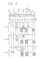
- the reset clock ⁇ R reaches its high level (5 V) at a time t1
- the on-state of the reset transistor 12 leads to the inflow of charges from the floating diffused region 7 to the reset drain region 9 and consequently a variation in the potential V RD there, but the variation in the potential V RD due to the inflow of charges can be ignored if the capacity of the capacitor C is sufficiently large.
- the reset clock ⁇ R drops to its low level, and at a time t3, a signal charge 40 flows into the floating diffused region 7.
- the voltage variation due to the inflow charge 40 into the floating diffused region 7 is guaranteed in a range of ⁇ B to ⁇ RL , as is apparent from FIG. 4, ⁇ RL being the channel potential beneath the reset gate electrode 8 when the reset clock ⁇ R is at its low level.
- ⁇ B - ⁇ RL will be 3.5 volts, because ⁇ RL is 7 volts according to FIG. 2. Since a 2 volt variation is usually considered sufficient, a wide enough dynamic range can be assured if the input voltage is 5 V.
- FIG. 5 shows a sectional view of a second preferred embodiment of the present invention.
- This embodiment differs from the first one in that the gate length of a barrier gate electrode 10a is 5 micron meters, equal to that of the reset gate electrode 8, and that a p-type barrier region 17 is formed beneath this barrier gate electrode 10a.
- the p-type barrier region 17 is 0.3 micron meters in depth, and its impurity concentration need not be higher than, or may be even half as high as, that of the p-type barrier region 3.
- the channel potential ⁇ B beneath the barrier gate electrode 10a is lower than the channel potential ⁇ RH beneath the reset gate electrode 8, which is the potential at the time when the reset clock ⁇ R is at its high level, so that charges in the floating diffused region 7 can be completely drained.
- the present invention makes it possible, by providing an absorption drain region via a barrier gate in a stage following the reset drain region connected to a capacitor, making the channel potential of the barrier gate lower than that under the reset gate electrode when in resetting operation, and providing a voltage booster whose output voltage is supplied to the absorption drain region, to obtain a charge transfer device free from the deterioration of the dynamic range resulting from faulty resetting of the floating diffused region even if the power voltage or the driving pulse supplied from outside is low in voltage. Since the charge transfer section may be prior art structure and requires no alteration, the voltage requirement can be lowered without entailing major redesigning.
Landscapes
- Solid State Image Pick-Up Elements (AREA)
Applications Claiming Priority (2)
| Application Number | Priority Date | Filing Date | Title |
|---|---|---|---|
| JP19023389 | 1989-07-21 | ||
| JP190233/89 | 1989-07-21 |
Publications (3)
| Publication Number | Publication Date |
|---|---|
| EP0409245A2 true EP0409245A2 (de) | 1991-01-23 |
| EP0409245A3 EP0409245A3 (en) | 1991-07-10 |
| EP0409245B1 EP0409245B1 (de) | 1997-03-12 |
Family
ID=16254709
Family Applications (1)
| Application Number | Title | Priority Date | Filing Date |
|---|---|---|---|
| EP90113876A Expired - Lifetime EP0409245B1 (de) | 1989-07-21 | 1990-07-19 | Mit verbesserter Ausgangsstruktur ausgestattetes Ladungstransfer-Bauelement |
Country Status (3)
| Country | Link |
|---|---|
| EP (1) | EP0409245B1 (de) |
| JP (1) | JPH07123163B2 (de) |
| DE (1) | DE69030142T2 (de) |
Cited By (2)
| Publication number | Priority date | Publication date | Assignee | Title |
|---|---|---|---|---|
| EP0766221A1 (de) * | 1995-09-29 | 1997-04-02 | Pioneer Electronic Corporation | Treiberschaltung für ein lichtemittierendes Element mit Switched-Capacitor-Netzwerk |
| US5777317A (en) * | 1994-05-27 | 1998-07-07 | Sony Corporation | Boosting circuit and solid-state image-sensing device employing said boosting circuit |
Families Citing this family (2)
| Publication number | Priority date | Publication date | Assignee | Title |
|---|---|---|---|---|
| JP3872927B2 (ja) * | 2000-03-22 | 2007-01-24 | 株式会社東芝 | 昇圧回路 |
| JP4641166B2 (ja) * | 2004-09-15 | 2011-03-02 | ルネサスエレクトロニクス株式会社 | 固体撮像装置の電荷転送デバイスおよび固体撮像装置の電荷転送デバイスの駆動方法 |
Family Cites Families (3)
| Publication number | Priority date | Publication date | Assignee | Title |
|---|---|---|---|---|
| US4513431A (en) * | 1982-06-07 | 1985-04-23 | International Business Machines Corporation | Charge coupled device output circuit structure |
| JP2508668B2 (ja) * | 1986-11-10 | 1996-06-19 | ソニー株式会社 | 電荷転送装置 |
| JPH084136B2 (ja) * | 1987-12-22 | 1996-01-17 | 日本電気株式会社 | 電荷転送装置 |
-
1990
- 1990-07-10 JP JP2182027A patent/JPH07123163B2/ja not_active Expired - Fee Related
- 1990-07-19 DE DE69030142T patent/DE69030142T2/de not_active Expired - Fee Related
- 1990-07-19 EP EP90113876A patent/EP0409245B1/de not_active Expired - Lifetime
Cited By (3)
| Publication number | Priority date | Publication date | Assignee | Title |
|---|---|---|---|---|
| US5777317A (en) * | 1994-05-27 | 1998-07-07 | Sony Corporation | Boosting circuit and solid-state image-sensing device employing said boosting circuit |
| EP0766221A1 (de) * | 1995-09-29 | 1997-04-02 | Pioneer Electronic Corporation | Treiberschaltung für ein lichtemittierendes Element mit Switched-Capacitor-Netzwerk |
| US5793163A (en) * | 1995-09-29 | 1998-08-11 | Pioneer Electronic Corporation | Driving circuit for light emitting element |
Also Published As
| Publication number | Publication date |
|---|---|
| JPH07123163B2 (ja) | 1995-12-25 |
| DE69030142T2 (de) | 1997-09-25 |
| EP0409245A3 (en) | 1991-07-10 |
| DE69030142D1 (de) | 1997-04-17 |
| JPH03129744A (ja) | 1991-06-03 |
| EP0409245B1 (de) | 1997-03-12 |
Similar Documents
| Publication | Publication Date | Title |
|---|---|---|
| US4321489A (en) | Voltage detection circuit | |
| US4228527A (en) | Electrically reprogrammable non volatile memory | |
| US5047816A (en) | Self-aligned dual-gate transistor | |
| JP2528794B2 (ja) | ラツチアツプ保護回路付き集積回路 | |
| US5825237A (en) | Reference voltage generation circuit | |
| US5191398A (en) | Charge transfer device producing a noise-free output | |
| JPH084136B2 (ja) | 電荷転送装置 | |
| JP2528795B2 (ja) | ラツチアツプ保護回路付き集積回路 | |
| US5306932A (en) | Charge transfer device provided with improved output structure | |
| US4455493A (en) | Substrate bias pump | |
| JPH04256361A (ja) | 半導体記憶装置 | |
| EP0409245A2 (de) | Mit verbesserter Ausgangsstruktur ausgestattetes Ladungstransfer-Bauelement | |
| JPH0152906B2 (de) | ||
| EP0248608A1 (de) | Ausgangspufferschaltungen | |
| EP0040377A2 (de) | Integrierte Schaltung zum Lesen und Schreiben von Informationen | |
| KR100278725B1 (ko) | 제1전압 부스팅 회로를 가진 집적회로 | |
| JPS6249991B2 (de) | ||
| JPH07105489B2 (ja) | 電荷転送装置 | |
| US4280067A (en) | Semiconductor charge transfer device having a decoupling gate for stopping reverse charge flow | |
| JPH07106553A (ja) | 固体撮像素子 | |
| JP2963572B2 (ja) | 電荷結合素子 | |
| JP3263197B2 (ja) | 電荷結合素子 | |
| EP0013117B1 (de) | Dynamische logische MOS-Schaltung | |
| JP2786665B2 (ja) | 電荷転送装置 | |
| JP2904962B2 (ja) | 昇圧装置 |
Legal Events
| Date | Code | Title | Description |
|---|---|---|---|
| PUAI | Public reference made under article 153(3) epc to a published international application that has entered the european phase |
Free format text: ORIGINAL CODE: 0009012 |
|
| 17P | Request for examination filed |
Effective date: 19900719 |
|
| AK | Designated contracting states |
Kind code of ref document: A2 Designated state(s): DE FR GB |
|
| PUAL | Search report despatched |
Free format text: ORIGINAL CODE: 0009013 |
|
| AK | Designated contracting states |
Kind code of ref document: A3 Designated state(s): DE FR GB |
|
| 17Q | First examination report despatched |
Effective date: 19931110 |
|
| GRAG | Despatch of communication of intention to grant |
Free format text: ORIGINAL CODE: EPIDOS AGRA |
|
| GRAH | Despatch of communication of intention to grant a patent |
Free format text: ORIGINAL CODE: EPIDOS IGRA |
|
| GRAH | Despatch of communication of intention to grant a patent |
Free format text: ORIGINAL CODE: EPIDOS IGRA |
|
| GRAA | (expected) grant |
Free format text: ORIGINAL CODE: 0009210 |
|
| AK | Designated contracting states |
Kind code of ref document: B1 Designated state(s): DE FR GB |
|
| REF | Corresponds to: |
Ref document number: 69030142 Country of ref document: DE Date of ref document: 19970417 |
|
| ET | Fr: translation filed | ||
| PLBE | No opposition filed within time limit |
Free format text: ORIGINAL CODE: 0009261 |
|
| STAA | Information on the status of an ep patent application or granted ep patent |
Free format text: STATUS: NO OPPOSITION FILED WITHIN TIME LIMIT |
|
| 26N | No opposition filed | ||
| PGFP | Annual fee paid to national office [announced via postgrant information from national office to epo] |
Ref country code: DE Payment date: 20010709 Year of fee payment: 12 |
|
| PGFP | Annual fee paid to national office [announced via postgrant information from national office to epo] |
Ref country code: FR Payment date: 20010712 Year of fee payment: 12 |
|
| PGFP | Annual fee paid to national office [announced via postgrant information from national office to epo] |
Ref country code: GB Payment date: 20010718 Year of fee payment: 12 |
|
| REG | Reference to a national code |
Ref country code: GB Ref legal event code: IF02 |
|
| PG25 | Lapsed in a contracting state [announced via postgrant information from national office to epo] |
Ref country code: GB Free format text: LAPSE BECAUSE OF NON-PAYMENT OF DUE FEES Effective date: 20020719 |
|
| PG25 | Lapsed in a contracting state [announced via postgrant information from national office to epo] |
Ref country code: DE Free format text: LAPSE BECAUSE OF NON-PAYMENT OF DUE FEES Effective date: 20030201 |
|
| GBPC | Gb: european patent ceased through non-payment of renewal fee |
Effective date: 20020719 |
|
| PG25 | Lapsed in a contracting state [announced via postgrant information from national office to epo] |
Ref country code: FR Free format text: LAPSE BECAUSE OF NON-PAYMENT OF DUE FEES Effective date: 20030331 |
|
| REG | Reference to a national code |
Ref country code: FR Ref legal event code: ST |