EP0410464A2 - Dispositif de mémoire à semiconducteur comportant un circuit de diagnostic pour cellules de mémoire - Google Patents
Dispositif de mémoire à semiconducteur comportant un circuit de diagnostic pour cellules de mémoire Download PDFInfo
- Publication number
- EP0410464A2 EP0410464A2 EP90114389A EP90114389A EP0410464A2 EP 0410464 A2 EP0410464 A2 EP 0410464A2 EP 90114389 A EP90114389 A EP 90114389A EP 90114389 A EP90114389 A EP 90114389A EP 0410464 A2 EP0410464 A2 EP 0410464A2
- Authority
- EP
- European Patent Office
- Prior art keywords
- diagnostic
- voltage level
- memory device
- diagnostic mode
- mode
- Prior art date
- Legal status (The legal status is an assumption and is not a legal conclusion. Google has not performed a legal analysis and makes no representation as to the accuracy of the status listed.)
- Granted
Links
Images


Classifications
-
- G—PHYSICS
- G11—INFORMATION STORAGE
- G11C—STATIC STORES
- G11C29/00—Checking stores for correct operation ; Subsequent repair; Testing stores during standby or offline operation
- G11C29/04—Detection or location of defective memory elements, e.g. cell constructio details, timing of test signals
- G11C29/50—Marginal testing, e.g. race, voltage or current testing
-
- G—PHYSICS
- G11—INFORMATION STORAGE
- G11C—STATIC STORES
- G11C29/00—Checking stores for correct operation ; Subsequent repair; Testing stores during standby or offline operation
- G11C29/04—Detection or location of defective memory elements, e.g. cell constructio details, timing of test signals
- G11C29/08—Functional testing, e.g. testing during refresh, power-on self testing [POST] or distributed testing
- G11C29/12—Built-in arrangements for testing, e.g. built-in self testing [BIST] or interconnection details
- G11C29/18—Address generation devices; Devices for accessing memories, e.g. details of addressing circuits
- G11C29/30—Accessing single arrays
- G11C29/34—Accessing multiple bits simultaneously
-
- G—PHYSICS
- G11—INFORMATION STORAGE
- G11C—STATIC STORES
- G11C11/00—Digital stores characterised by the use of particular electric or magnetic storage elements; Storage elements therefor
- G11C11/21—Digital stores characterised by the use of particular electric or magnetic storage elements; Storage elements therefor using electric elements
- G11C11/34—Digital stores characterised by the use of particular electric or magnetic storage elements; Storage elements therefor using electric elements using semiconductor devices
- G11C11/40—Digital stores characterised by the use of particular electric or magnetic storage elements; Storage elements therefor using electric elements using semiconductor devices using transistors
- G11C11/401—Digital stores characterised by the use of particular electric or magnetic storage elements; Storage elements therefor using electric elements using semiconductor devices using transistors forming cells needing refreshing or charge regeneration, i.e. dynamic cells
-
- G—PHYSICS
- G11—INFORMATION STORAGE
- G11C—STATIC STORES
- G11C29/00—Checking stores for correct operation ; Subsequent repair; Testing stores during standby or offline operation
- G11C29/04—Detection or location of defective memory elements, e.g. cell constructio details, timing of test signals
- G11C29/50—Marginal testing, e.g. race, voltage or current testing
- G11C2029/5004—Voltage
Definitions
- This invention relates to a semiconductor memory device and, more particularly, to a diagnostic circuit incorporated in the semiconductor memory device.
- semiconductor memory devices are subjected to a diagnostic operation prior to delivery from the factory.
- diagnostic operation all of the memory cells are examined to see whether the individual memory cells are perfect or defective, and, for this reason, time period consumed per a chip is increased with the integration density.
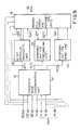
- the diagnostic circuit shown in Fig. 1 is incorporated in a 4 mega-bit dynamic random access memory device and comprises a mode discriminating unit 1, an eight-bit parallel diagnostic unit 2 and a memory cell array associated with peripheral units 3.
- the mode discriminating unit 1 is supplied with a row address strobe signal RAS , a column address strobe signal CAS and a write enable signal WE , and a diagnostic mode of operation is requested at a CAS -before- RAS refresh timing in the presence of the write enable signal WE of an active low voltage level.
- the column address strobe signal CAS is shifted to the active low voltage level at time t1, and the row address strobe signal RAS enters the active low voltage level at time t2 as shown in Fig. 2.
- the mode discriminating unit 1 acknowledges the request for the diagnostic mode of operation and allows a diagnostic mode signal DGM to go up to an active high voltage level.
- the diagnostic mode signal DGM is supplied in parallel to the eight-bit parallel diagnostic unit 2 and the memory cell array 3. With the diagnostic mode signal DGM, the eight-bit diagnostic unit 2 is activated, and data bits are sequentially read out from the memory cell array 3.
- the data bits are transferred from the memory cell array 3 to the eight-bit parallel diagnostic unit 2 through an eight-bit read-and-write bus RWB, and every eight data bits are simultaneously examined to see whether any one of the eight data bits is indicative of a defect or not. Since a data bit of a predetermined logic level has been written into all of the memory cells, the eight-bit parallel diagnostic unit 2 decides that the semiconductor memory device is of the inferior product upon discrepancy between the eight data bits and shifts a fail signal DGF to the active high voltage level. With the fail signal DGF, one of the peripheral units associated with the memory cell array 3 allows a data output terminal Dout to enter the high impedance state. The data output terminal Dout is monitored from the outside during the diagnostic operation, and the high impedance state tells of the defect found through the diagnostic operation.
- the prior art diagnostic technology decreases the amount of time consumed for the diagnostic operation.
- the eight bit parallel diagnostic unit 2 shrinks the time period to a eighth of that achieved by a single bit diagnostic unit.
- the number of items to be examined is generally n 2 times larger than that of the previous generation. For this reason, the eight bit parallel diagnostic unit 2 is less effective to a semiconductor memory device of the next generation.
- the inventor analyzes the diagnostic items to see what item consumes a relatively long time and why that item consumes the time.
- the 4-mega bit dynamic random access memory device guarantees the maximum cycle time of 10 micro-second which is fifty times longer than the minimum cycle time.
- the memory cell array is innocent of any defect on the time consuming, but some peripheral units associated with the memory cell array directly concern it.
- Fig. 3 shows an essential part of the prior art dynamic random access memory device shown in Fig. 1 in an enlarged scale.
- the memory cell array incorporated in the dynamic random access memory device consists of a large number of, typically four million one hundred and ninety thousand, bits, and the memory cells are of the one-transistor and one-capacitor type.
- One of the memory cells is abbreviated as "MC11" and coupled to a bit line pair BLP consisting of a bit line BL1 and a dummy bit line BL2.
- An electric source 31 is coupled through a power line HFV to a switching element array and equalizer 32 which precharge and balance bit line pairs including the bit line pair BLP.
- the memory cell array is further coupled to word lines including a word line WL1, and the word lines are selectively driven by a row address decoder circuit 33 coupled to an electric source 34.
- the bit line pair BLP is coupled to a sense amplifier circuit 35, and the sense amplifier circuit 35 increases a difference in voltage level between the bit line Bl1 and the dummy bit line BL2 for quick decision.
- the short circuiting is hardly found because the bit line pair BLP is well balanced due to the electric charges discharged upon the equalization.
- the bit line pair BLP is maintained in a predetermined intermediate voltage level over the minimum cycle time regardless of the short circuit between the power line HFV and the conductive node.
- the short circuiting allows current more than that of the electric source 31 to flow, the intermediate voltage level fluctuates and the sense amplifier circuit 35 fails in the differential amplification. This failure is detected by the eight-bit discriminating unit 1, and the dynamic random access memory device is rejected as an inferior product.
- Another defect detectable in the maximum cycle time resides in the electric source 34.
- the word lines are driven at a predetermined high voltage level, and the predetermined high voltage level is produced through a bootstrapping.
- the defect in the electric source 34 is hardly detectable in a diagnostic operation on the minimum cycle time due to the bootstrapped high voltage level but is detectable in the diagnostic operation on the maximum cycle time. The same problem is encountered in the diagnostic operation as described hereinbefore.
- the prior art diagnostic technology has problems in a prolonged time period consumed in the diagnostic operation and in a reliability of the diagnostic technology.
- the present invention proposes to directly compare voltage levels at predetermined points in a semiconductor memory device with respective standard values in a diagnostic mode of operation.
- a semiconductor memory device having a usual mode and a diagnostic mode of operation for detecting a defective portion, comprising: a) a diagnostic mode discriminating unit responsive to external control signals indicative of a request for the diagnostic mode of operation and producing first and second activation signals; b) a memory cell array having a plurality of memory cells and associat ed with a plurality of peripheral units for carrying out the usual mode and the diagnostic mode of operation, the memory cells storing respective data bits, the peripheral units having a conductive portion liable to be affected by a defect; c) a multi-bit parallel diagnostic unit responsive to the first activation signal and causing the memory cell array associated with the peripheral units to sequentially supply a plurality of data bit groups each consisting of a predetermined number of the data bits thereto for detecting a defective portion having an influence on the data bits; and d) voltage level examining means responsive to the second activation signal and comparing
- a dynamic random access memory device embodying the present invention is fabricated on a semiconductor chip 41 and comprises a diagnostic mode discriminating unit 42, an eight-bit parallel diagnostic unit 43, an examining unit for precharging level 44 and a memory cell array associated with peripheral units 45.
- the diagnostic mode discriminating unit 42 is supplied with a row address strobe signal RAS , a column address strobe signal CAS , a write enable signal WE and two address bits A0 and A1 of an address signal ADD, and discriminates a diagnostic mode of operation at the CAS -before- RAS refresh timing in the presence of the write enable signal WE of an active low voltage level.
- the diagnostic mode discriminating unit 42 acknowledges a request for a diagnostic operation in the presence of the write enable signal WE of the active low voltage level at time t12 as shown in Fig. 5.
- the diagnostic mode discriminating unit 42 selectively drives first and second activation signals ACT1 and ACT2 depending upon a combination of the address bits A0 and A1.
- the diagnostic mode discriminating unit 42 shifts only the second activation signal ACT2 to the active level and allows the examining unit 44 to carry out an examination for a precharging level as described hereinlater. However, if both of the address bits A0 and A1 are in the high voltage level, the diagnostic mode discriminating unit 42 drives not only the first activation signal ACT1 but also the second activation signal ACT2 to the active level.
- the memory cell array 45a has a plurality of memory cells, and only two memory cells are designated by MC11 and MC21, respectively. All of the memory cells are of the type having one-transistor and one-capacitor, and a plurality of bit lines including bit lines BL1 and BL2 are coupled to the memory cells.
- the bit lines are precharged and balanced by a combined circuit 45b of a switching element array and an equalizer, and the switching element array provides and blocks current paths between an electric source 45c and the bit lines.
- a current path between the electric source 45c and the switching element array is designated by a reference mark HFV.
- the memory cells are further coupled to a plurality of word lines WL1 to WLn, and the word lines WL1 to WLn are selectively driven by a row address decoder circuit 45d.
- An electric source 45e is coupled to the row decoder circuit 45d and supplies a high voltage produced through a bootstrapping to the row address circuit 45d.
- the row address decoder circuit 45d drives one of the word lines WL1 to WLn, data bits are read out from the memory cells coupled to the selected word line to the bit lines.
- bit line BL1 is paired with the bit line BL2 to form a bit line pair BLP1, and other bit lines are also paired with one another to form bit line pairs.
- a sense amplifier circuit 45f is coupled to the bit line pair BLP1, and the other bit line pairs are also coupled to sense amplifier circuits (not shown).
- the sense amplifier circuit 45f increases a small difference in voltage level between the bit lines BL1 and BL2 for quick determination in logic level.
- the other sense amplifier circuits behaves as similar to the sense amplifier circuit 45f.
- One of the data bits thus determined in logic level is transferred through a suitable selector circuit to a tri-state output buffer circuit 48g, and the tri-state output buffer circuit 48g drives a data pin Dout depending upon the logic level of the selected data bit.
- the tri-state output buffer circuit 48g is associated with an OR gate 48h, and the OR gate 48h allows the data pin Dout to enter a high impedance stated
- the memory cell array 45a is further associated with various peripheral units or circuits; however, no further description is incorporated hereinbelow because such units and circuits are well known.
- the dynamic random access memory device shown in Fig. 4 selectively enter a diagnostic mode of operation and a usual mode of operation, i.e. a read-out mode of operation and a write-in mode of operation.
- a diagnostic mode of operation i.e. a read-out mode of operation and a write-in mode of operation.
- a usual mode of operation i.e. a read-out mode of operation and a write-in mode of operation.
- description for the usual mode of operation is omitted because of similarity to the prior art dynamic random access memory device.
- the eight bit parallel diagnostic unit 43 is similar to those of the dynamic memory device shown in Fig. 1. Namely, the first activation signal ACT1 is supplied in parallel to the eight-bit parallel diagnostic unit 43 and the memory cell array associated with the peripheral units 45. With the first activation signal ACT1, the eight-bit diagnostic unit 43 is activated, and data bits are sequentially read out from the memory cell array 45a. The data bits are transferred from the memory cell array 45a to the eight-bit parallel diagnostic unit 43 through an eight-bit read-and-write bus RWB, and every eight data bits are simultaneously examined to see whether any one of the eight data bits is indicative of a defect or not.
- the eight-bit parallel diagnostic unit 2 decides that the dynamic random access memory device is of the inferior product upon discrepancy between the eight data bits and shifts a first fail signal DGF1 to the active high voltage level.
- the first fail signal DGF1 is relayed through the OR gate 48h to the tri-state output buffer circuit 48g, and the tri-state output buffer circuit 48g allows the data pin Dout to enter the high impedance state.
- the data pin Dout is monitored from the outside during the diagnostic operation, and the high impedance state tells of the defect found through the diagnostic operation.
- the examining unit for precharging level 44 is responsive to the second activation signal ACT2 and checks a voltage level Vnd at a node ND on the power line HFV to see whether or not any variation takes place. If a defect has an influence on the precharging voltage level on the bit line pair BLP1, the voltage level Vnd at the node ND is different from a standard level.
- the examining circuit 44 notices the defect taking place through comparison of the voltage level Vnd with reference voltage signals Ref1 and Ref2 indicative of an acceptable range, and shifts a second fail signal DGF2 to an active level.
- the second fail signal DGF2 passes through the OR gate 48h and reaches the tri-state output buffer circuit 48g.
- the tri-state output buffer circuit 48g allows the data pin Dout to enter the high impedance state. Then, the external monitor recognizes the defect, and, accordingly, the dynamic random access memory device is rejected as a inferior product.
- a typical example of the defect having an influence on the precharging level is a short circuiting in the electric source 45c, however, various defects are detectable through monitoring the voltage level Vnd in so far as the precharging voltage level reaches the defective point.
- Fig. 7 shows the arrangement of the examining circuit 44 comprising a reference signal producing circuit 48a, two comparators 48b and 48c and a fail signal producing circuit 48d.
- the reference signal producing circuit 48a has an upper bound level setting section 48e for producing the reference signal Ref1 indicative of the upper bound value of the acceptable range, and a lower bound level setting section 48f for producing the reference signal Ref2 indicative of the lower bound value of the acceptable range.
- the fail signal producing circuit is implemented by an OR gate.
- Each of the upper bound level setting section 48e and the lower bound level setting section 48f is arranged as shown in Fig. 8 and comprises a first series combination of a first resistor R1, second and third field effect transistors Q1 and Q2 and a second resistor R2 coupled between a source of positive voltage level Vdd and a ground node, and a second series combination of third and fourth field effect transistors Q3 and Q4 coupled between the source of positive voltage level Vdd and the ground node.
- the first and second field effect transistors are an n-channel type, but the second and fourth field effect transistors Q2 and Q4 are a p-channel type.
- the voltage level at a node N1 is adjustable by selecting the resistances of the first and second resistors R1 and R2, and the voltage level at the node N1 is relayed to a node N2, because gate voltage levels at nodes N3 and N4 are shared between the n-channel type field effect transistors Q1 and Q3 and between the n-channel type field effect transistors Q2 and Q4, respectively.
- the second series combination is larger in current driving capability than the first series combination, and, for this reason, the reference signal Ref1 or Ref2 is large enough for the comparator 48b or 48c.
- the ratio of the first resistor R1 to the second resistor R2 is different between the upper bound level setting section 48e and the lower bound setting section 48f, and, accordingly, the reference signals Ref1 and Ref2 are different in voltage level from one another.
- the comparators 48b and 48c are activated in the presence of the second activation signal ACT2 and compares the voltage level Vnd with the reference signals Ref1 and Ref2, respectively. If the voltage level Vnd is higher than the reference signal Ref1 or lower than the reference signal Ref2, the voltage level Vnd is out of the acceptable range, and, accordingly, the fail signal producing circuit 48d shifts the second fail signal DGF2 to the active level.
- the electric source 45c has the same circuit arrangement as the upper bound level setting section 48e or the lower bound level setting section 48f, and any short circuiting is such a circuit arrangement is causative of the variation of the precharging voltage level.
- the examining circuit 48 thus arranged is effective in decreasing the time period for the diagnostic operation as well as in enhancing the reliability of the dynamic random access memory device. If the examining circuit 48 is activated with the address bits A0 and A1 of the high voltage level, any defect with influence on the precharging level is directly detected within an extremely short time period. Such a quick detection speeds up the diagnostic operation. Since the variation in the precharging voltage level is directly detected, the diagnostic operation enhances the reliability of the dynamic random access memory device. Moreover, only a single examination is enough for the diagnostic operation on the precharging voltage level, because the variation in precharging voltage level is independent of the memory cells and the sense amplifier circuits. If the random access memory device is of the four-mega bit type, the diagnostic operation is decreased to an extremely short time period which is one five hundred thousandth of that consumed by the prior art four-mega bit dynamic random access memory device.
- FIG. 9 of the drawings another dynamic random access memory device is illustrated and has all of the component units 42, 43, 44 and 45 of the dynamic random access memory device shown in Fig. 4.
- the diagnostic mode discriminating unit 42 produces not only the first and second activation signals ACT1 and ACT2 but also a third activation signal ACT3 depending upon a combination of address bits A0, A1 and A2.
- the dynamic random access memory device shown in Fig. 9 further comprises another examining unit 101 which examines a voltage level Vwd on the word lines WL1 to WLn in the presence of the third activation signal ACT3. If a defect takes place in the electric source 45e by way of example, the voltage level Vwd on the word line is varied from a standard range.
- the examining unit 101 detects the voltage level Vwd out of the standard range as similar to the examining unit 44 and shift a third fail signal DGF3 to an active level. With the third fail signal DGF3, the tri-state output buffer circuit 48g allows the data pin Dout to enter the high impedance state.
- the examining unit 101 is similar in circuit arrangement to the examining unit 44, and, for this reason, no further description is incorporated for the sake of simplicity.
- the examining unit 101 is valuable for a semiconductor memory device having the electric source 45e for boot-strapping a voltage level fed from the outside thereof, because a defect having an influence on the voltage level on the word line tends to takes place in the electric source 45e.
- the semiconductor devices described hereinbefore are of the random access memory, however, the present invention is applicable to a semiconductor memory device of another type such as, for example, an electrically erasable programmable read only memory.
Landscapes
- For Increasing The Reliability Of Semiconductor Memories (AREA)
- Dram (AREA)
- Techniques For Improving Reliability Of Storages (AREA)
- Tests Of Electronic Circuits (AREA)
Applications Claiming Priority (2)
| Application Number | Priority Date | Filing Date | Title |
|---|---|---|---|
| JP1195458A JPH0359899A (ja) | 1989-07-27 | 1989-07-27 | 半導体メモリ |
| JP195458/89 | 1989-07-27 |
Publications (3)
| Publication Number | Publication Date |
|---|---|
| EP0410464A2 true EP0410464A2 (fr) | 1991-01-30 |
| EP0410464A3 EP0410464A3 (en) | 1992-01-02 |
| EP0410464B1 EP0410464B1 (fr) | 1994-09-28 |
Family
ID=16341408
Family Applications (1)
| Application Number | Title | Priority Date | Filing Date |
|---|---|---|---|
| EP19900114389 Expired - Lifetime EP0410464B1 (fr) | 1989-07-27 | 1990-07-26 | Dispositif de mémoire à semiconducteur comportant un circuit de diagnostic pour cellules de mémoire |
Country Status (3)
| Country | Link |
|---|---|
| EP (1) | EP0410464B1 (fr) |
| JP (1) | JPH0359899A (fr) |
| DE (1) | DE69012913T2 (fr) |
Cited By (5)
| Publication number | Priority date | Publication date | Assignee | Title |
|---|---|---|---|---|
| EP0520356A1 (fr) * | 1991-06-25 | 1992-12-30 | Nec Corporation | Circuit intégré à semi-conducteur équipé d'un circuit de diagnostic |
| EP0520696A3 (en) * | 1991-06-27 | 1993-10-27 | Nec Corp | Semiconductor memory/integrated circuit device with discriminator for diagnostic mode of operation |
| EP0455977A3 (fr) * | 1990-03-30 | 1995-02-08 | Nippon Electric Co | |
| SG79979A1 (en) * | 1997-06-13 | 2001-04-17 | Advantest Corp | Semiconductor integrated circuit testing apparatus |
| CN101452010B (zh) * | 2007-11-30 | 2011-12-14 | 上海华虹Nec电子有限公司 | 用于芯片测试的探针卡的测试方法 |
Family Cites Families (1)
| Publication number | Priority date | Publication date | Assignee | Title |
|---|---|---|---|---|
| US4393475A (en) * | 1981-01-27 | 1983-07-12 | Texas Instruments Incorporated | Non-volatile semiconductor memory and the testing method for the same |
-
1989
- 1989-07-27 JP JP1195458A patent/JPH0359899A/ja active Pending
-
1990
- 1990-07-26 DE DE1990612913 patent/DE69012913T2/de not_active Expired - Fee Related
- 1990-07-26 EP EP19900114389 patent/EP0410464B1/fr not_active Expired - Lifetime
Cited By (5)
| Publication number | Priority date | Publication date | Assignee | Title |
|---|---|---|---|---|
| EP0455977A3 (fr) * | 1990-03-30 | 1995-02-08 | Nippon Electric Co | |
| EP0520356A1 (fr) * | 1991-06-25 | 1992-12-30 | Nec Corporation | Circuit intégré à semi-conducteur équipé d'un circuit de diagnostic |
| EP0520696A3 (en) * | 1991-06-27 | 1993-10-27 | Nec Corp | Semiconductor memory/integrated circuit device with discriminator for diagnostic mode of operation |
| SG79979A1 (en) * | 1997-06-13 | 2001-04-17 | Advantest Corp | Semiconductor integrated circuit testing apparatus |
| CN101452010B (zh) * | 2007-11-30 | 2011-12-14 | 上海华虹Nec电子有限公司 | 用于芯片测试的探针卡的测试方法 |
Also Published As
| Publication number | Publication date |
|---|---|
| EP0410464A3 (en) | 1992-01-02 |
| EP0410464B1 (fr) | 1994-09-28 |
| DE69012913T2 (de) | 1995-05-04 |
| JPH0359899A (ja) | 1991-03-14 |
| DE69012913D1 (de) | 1994-11-03 |
Similar Documents
| Publication | Publication Date | Title |
|---|---|---|
| EP0638902B1 (fr) | Circuit de sélection, sélectionnant et générant une tension appliquée à l'un ou l'autre terminal en réponse au niveau de tension appliquée au premier terminal | |
| US5563832A (en) | Semiconductor memory device having interface units memorizing available memory cell sub-arrays | |
| US6424142B1 (en) | Semiconductor device operable in a plurality of test operation modes | |
| US5079744A (en) | Test apparatus for static-type semiconductor memory devices | |
| US6819611B2 (en) | Method and apparatus for data compression in memory devices | |
| US5436911A (en) | Semiconductor memory device comprising a test circuit and a method of operation thereof | |
| US5185722A (en) | Semiconductor memory device having a memory test circuit | |
| US6327200B1 (en) | Circuit and method for testing a memory device | |
| US5523977A (en) | Testing semiconductor memory device having test circuit | |
| EP0920032B1 (fr) | Mémoire ferroélectrique à accès aléatoire avec détecteur éphémère de cellules pour tester un condensateur ferroélectrique et procédé de test de cellules ferroélectriques de mémoire | |
| KR20040092801A (ko) | 반도체 메모리 장치 | |
| KR19990078380A (ko) | 반도체 메모리 테스트 방법 및 장치 | |
| US5745499A (en) | Supervoltage detection circuit having a multi-level reference voltage | |
| US6501691B2 (en) | Word-line deficiency detection method for semiconductor memory device | |
| US5742549A (en) | Sense amplifier circuit for detecting degradation of digit lines and method thereof | |
| KR100367191B1 (ko) | 테스트수단을구비한전자회로및메모리셀테스트방법 | |
| JP2008522334A (ja) | ウィークセルを検出するためのsram検査方法とsram検査装置 | |
| US6172925B1 (en) | Memory array bitline timing circuit | |
| US20040062096A1 (en) | Rapidly testable semiconductor memory device | |
| EP0410464B1 (fr) | Dispositif de mémoire à semiconducteur comportant un circuit de diagnostic pour cellules de mémoire | |
| US5091884A (en) | Semiconductor memory device with improved address discriminating circuit for discriminating an address assigned defective memory cell replaced with redundant memory cell | |
| US5088063A (en) | Semiconductor memory device having on-chip test circuit | |
| US5184327A (en) | Semiconductor memory device having on-chip test circuit and method for testing the same | |
| US6317368B1 (en) | Semiconductor integrated circuit device tested in batches | |
| US5365482A (en) | Semiconductor memory device with provision of pseudo-acceleration test |
Legal Events
| Date | Code | Title | Description |
|---|---|---|---|
| PUAI | Public reference made under article 153(3) epc to a published international application that has entered the european phase |
Free format text: ORIGINAL CODE: 0009012 |
|
| 17P | Request for examination filed |
Effective date: 19900726 |
|
| AK | Designated contracting states |
Kind code of ref document: A2 Designated state(s): DE FR GB |
|
| PUAL | Search report despatched |
Free format text: ORIGINAL CODE: 0009013 |
|
| AK | Designated contracting states |
Kind code of ref document: A3 Designated state(s): DE FR GB |
|
| 17Q | First examination report despatched |
Effective date: 19940107 |
|
| GRAA | (expected) grant |
Free format text: ORIGINAL CODE: 0009210 |
|
| AK | Designated contracting states |
Kind code of ref document: B1 Designated state(s): DE FR GB |
|
| REF | Corresponds to: |
Ref document number: 69012913 Country of ref document: DE Date of ref document: 19941103 |
|
| ET | Fr: translation filed | ||
| PGFP | Annual fee paid to national office [announced via postgrant information from national office to epo] |
Ref country code: GB Payment date: 19950725 Year of fee payment: 6 Ref country code: FR Payment date: 19950725 Year of fee payment: 6 |
|
| PLBE | No opposition filed within time limit |
Free format text: ORIGINAL CODE: 0009261 |
|
| STAA | Information on the status of an ep patent application or granted ep patent |
Free format text: STATUS: NO OPPOSITION FILED WITHIN TIME LIMIT |
|
| 26N | No opposition filed | ||
| PGFP | Annual fee paid to national office [announced via postgrant information from national office to epo] |
Ref country code: DE Payment date: 19950920 Year of fee payment: 6 |
|
| PG25 | Lapsed in a contracting state [announced via postgrant information from national office to epo] |
Ref country code: GB Effective date: 19960726 |
|
| GBPC | Gb: european patent ceased through non-payment of renewal fee |
Effective date: 19960726 |
|
| PG25 | Lapsed in a contracting state [announced via postgrant information from national office to epo] |
Ref country code: FR Effective date: 19970328 |
|
| PG25 | Lapsed in a contracting state [announced via postgrant information from national office to epo] |
Ref country code: DE Effective date: 19970402 |
|
| REG | Reference to a national code |
Ref country code: FR Ref legal event code: ST |