EP0411612A2 - Dispositif émetteur de lumiÀ¨re à semi-conducteur - Google Patents
Dispositif émetteur de lumiÀ¨re à semi-conducteur Download PDFInfo
- Publication number
- EP0411612A2 EP0411612A2 EP90114775A EP90114775A EP0411612A2 EP 0411612 A2 EP0411612 A2 EP 0411612A2 EP 90114775 A EP90114775 A EP 90114775A EP 90114775 A EP90114775 A EP 90114775A EP 0411612 A2 EP0411612 A2 EP 0411612A2
- Authority
- EP
- European Patent Office
- Prior art keywords
- area
- type semiconductor
- semiconductor layer
- emitting device
- junction
- Prior art date
- Legal status (The legal status is an assumption and is not a legal conclusion. Google has not performed a legal analysis and makes no representation as to the accuracy of the status listed.)
- Granted
Links
Images


Classifications
-
- H—ELECTRICITY
- H10—SEMICONDUCTOR DEVICES; ELECTRIC SOLID-STATE DEVICES NOT OTHERWISE PROVIDED FOR
- H10H—INORGANIC LIGHT-EMITTING SEMICONDUCTOR DEVICES HAVING POTENTIAL BARRIERS
- H10H20/00—Individual inorganic light-emitting semiconductor devices having potential barriers, e.g. light-emitting diodes [LED]
- H10H20/80—Constructional details
- H10H20/81—Bodies
- H10H20/819—Bodies characterised by their shape, e.g. curved or truncated substrates
- H10H20/821—Bodies characterised by their shape, e.g. curved or truncated substrates of the light-emitting regions, e.g. non-planar junctions
-
- H—ELECTRICITY
- H10—SEMICONDUCTOR DEVICES; ELECTRIC SOLID-STATE DEVICES NOT OTHERWISE PROVIDED FOR
- H10H—INORGANIC LIGHT-EMITTING SEMICONDUCTOR DEVICES HAVING POTENTIAL BARRIERS
- H10H20/00—Individual inorganic light-emitting semiconductor devices having potential barriers, e.g. light-emitting diodes [LED]
- H10H20/01—Manufacture or treatment
- H10H20/011—Manufacture or treatment of bodies, e.g. forming semiconductor layers
- H10H20/014—Manufacture or treatment of bodies, e.g. forming semiconductor layers having light-emitting regions comprising only Group IV materials
-
- H—ELECTRICITY
- H10—SEMICONDUCTOR DEVICES; ELECTRIC SOLID-STATE DEVICES NOT OTHERWISE PROVIDED FOR
- H10H—INORGANIC LIGHT-EMITTING SEMICONDUCTOR DEVICES HAVING POTENTIAL BARRIERS
- H10H20/00—Individual inorganic light-emitting semiconductor devices having potential barriers, e.g. light-emitting diodes [LED]
- H10H20/052—Light-emitting semiconductor devices having Schottky type light-emitting regions; Light emitting semiconductor devices having Metal-Insulator-Semiconductor type light-emitting regions
-
- H—ELECTRICITY
- H10—SEMICONDUCTOR DEVICES; ELECTRIC SOLID-STATE DEVICES NOT OTHERWISE PROVIDED FOR
- H10H—INORGANIC LIGHT-EMITTING SEMICONDUCTOR DEVICES HAVING POTENTIAL BARRIERS
- H10H20/00—Individual inorganic light-emitting semiconductor devices having potential barriers, e.g. light-emitting diodes [LED]
- H10H20/80—Constructional details
- H10H20/81—Bodies
-
- H—ELECTRICITY
- H10—SEMICONDUCTOR DEVICES; ELECTRIC SOLID-STATE DEVICES NOT OTHERWISE PROVIDED FOR
- H10H—INORGANIC LIGHT-EMITTING SEMICONDUCTOR DEVICES HAVING POTENTIAL BARRIERS
- H10H20/00—Individual inorganic light-emitting semiconductor devices having potential barriers, e.g. light-emitting diodes [LED]
- H10H20/80—Constructional details
- H10H20/81—Bodies
- H10H20/822—Materials of the light-emitting regions
- H10H20/824—Materials of the light-emitting regions comprising only Group III-V materials, e.g. GaP
- H10H20/8242—Materials of the light-emitting regions comprising only Group III-V materials, e.g. GaP characterised by the dopants
Definitions
- the present invention relates to a semiconductor light-emitting device which has a planar type PN junction or a Schottky junction and produces a light by applying a reverse bias to the junction to cause an avalanche breakdown.
- Photo-emission from avalanche breakdown has been reported by an article "Photo emission from avalanche breakdown” by A.G. Chynoweth and H.K. Mckey, Phys. Rev., Vol. 102, p.369, 1956.
- an application of the photo emission phenomenon to a light emitting semiconductor element is reported in "A study of the nature and characteristics of light radiation in reverse-biased silicon junctions” by C.B. Williams and K. Daneshver, Conf. Proc. IEEE, sou theostion, p.161, 1988.
- a photo emission intensity on a Si PN junction interface is 0.01 W/cm2.
- the semiconductor devices in those articles comprise planar type PN junctions as described in "Physics of Semiconductor Devices" by S.M. Sze, John Wiley & Sons, p.73.
- a semiconductor light emitting device comprising: a substrate; an n-type semiconductor layer formed on said substrate; a p-type semiconductor layer formed on a portion of a surface of said n-type semiconductor layer; said p-type semiconductor layer forming a planar type PN junction with said n-type semiconductor layer; an electorde for applying a reverse biasing voltage to said PN junction to cause an avalanche breakdown; and an area formed in a portion of said PN junction; said area having a lower breakdown voltage than that of other area.
- a semiconductor light emitting device comprising: a substrate; an n-type semiconductor layer formed on said substrate; a Schottky electrode layer formed on said n-type semiconductor layer; said Schottky electrode layer forming a Schottky junction with the n-type semiconductor layer; a contact electrode for applying a reverse biasing voltage to said Schottky junction to cause an avalanche breakdown; and an area formed in a portion of said Schottky junction; said area having a lower breakdown voltage than other area.
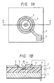
- Figs. 1A and 1B show a plan view and an A-A′ sectional view of a first embodiment of the semiconductor light emitting device of the present invention. This device manufactured by the following process.
- n-type semiconductor layer 2 having an impurity concentration of 3 ⁇ 1016 cm ⁇ 3 was formed on an n-type semiconductor substrate 1 (GaAs (100) in the present embodiment) by monochrome beam epitaxy (MBE) growth.
- Photoresist in an area 3 is cut by a photolithography resist process, and Si ions were injected therein at an acceleration voltage of 80 KeV.
- photoresist in an area 5 was cut by a similar resist process and Zn ions were injected therein at an acceleration voltage of 40 KeV.
- the area 3 was rendered to a highly doped n-type area having a peak impurity concentration of approximately 1 ⁇ 1018 cm ⁇ 3, and the area 5 to a p-type semiconductor layer having a peak impurity concentration of no smaller than approximately 1 ⁇ 1019 cm ⁇ 3.
- the size of the highly doped n-type area 3 is preferably no larger than 5 ⁇ m in diameter. When it is larger than 5 ⁇ m, a uniform light emission is not attained and heat generation increases.
- the thickness of the p-type semiconductor layer is preferably no larger than 0.1 ⁇ m. If it is larger than 0.1 ⁇ m, a light transmittance rapidly decreases.
- SiO2 was sputtered on the semiconductor layer to form an insulation layer 9.
- Photoresist at a predetermined position was cut by the same resist process as that described above and a portion of the insulation layer 9 was etched off to form an opening.
- Cr/Au was vapor-deposited thereon and unnecessary portion was removed by etching, and an ohmic contact electrode 6 to the p-type semiconductor was formed.
- An Al contact electrode 11 was formed to be connected to the electrode 6.
- An ohmic contact electrode 8 was formed on a bottom surface of the substrate 1.
- a reverse biasing electric field was applied to the device thus formed from a power supply 7 through electrodes 6 and 8 so that a light h ⁇ was emitted from the top of the area 3.
- Fig. 2 shows an energy band of the semiconductor light emitting device of the present invention.
- Fig. 2 by jointing the p-type semiconductor layer to the n-type semiconductor layer and applying the reverse bias to cause the avalanche breakdown, a number of electrons and holes are generated in a depletion layer.
- the generated electrons and holes cause not only a normal inter-band transition shown by a in Fig. 3 but also a recombination of carriers having a high energy shown by b or an intra-band transition shown by c , and the light is emitted.
- the highly doped n-type area 3 which is distinctive from other area is formed in the n-type semiconductor layer 2 to from a depletion layer shown by a broken line 4 in Fig. 1B.
- An uniform and high electric field area is formed throughout the highly doped n-type area 3 so that the light emission uniformly occurs only in the highly doped area.
- the high electric field is formed to increase an electron-hole pair generation efficiency to increase the light emission probability and attain a brightness control. Further, by applying a high energy to the electrons-holes, a light having a larger energy than a band gap Eg is emitted.
- the n-type semiconductor is used as the semiconductor substrate.
- a highest electric field is formed below the p-type semiconductor which is exposed to the surface, and the electrons which are minority carriers in the p-type semiconductor most act on the avalanche amplification.
- a substrate for example, silicon
- the electron-hole pair generation efficiency varies depending on the type of carriers and the probability of generation of the electron-hole pairs by the electron is larger than the probability of generation of the electron-hole pairs by the holes
- the electron generation efficiency is improved by the present embodiment.
- the thickness of the p-type semiconductor layer is very thin enough to fully transmit the light generated at the PN junction interface and reduce a light transmission loss.
- a light emitting device having a relation between the photon energy and the light intensity as shown in Fig. 4 is manufactured with a high control.
- Fig. 5 shows a second embodiment of the present invention.
- Fig. 5 shows a sectional view of the device as Fig. 1B does.
- the like elements to those shown in Fig. 1B are designated by the like numerals.
- the device was manufactured in the following process.
- n-type semiconductor layer 2 having an impurity concentration of 5 ⁇ 1016 cm ⁇ 3 was epitaxially grown on an n-type semiconductor substrate (Si (100) in the present embodiment) by a vapor deposition (CVD) method. Then, SiO2 was formed to a thickness of 4000 ⁇ by thermal diffusion, and resist at a predetermined position was cut by a resist process and SiO2 was removed by fluodic acid etchant to form a donut-shaped opening on the top of the area 10. Then, B (boron) was thermal-diffused by appropriate dopant to form a p-type guard ring area 10. Then, the SiO2 area at the top of the light emission area was removed by the resist process and the etchant.
- P ions (phosphorus) were injected into the area 3 and Ga(galium) ions were injected into the area 5 to make the area 3 to the n-type semiconductor having a peak impurity concentration of approximately 8 ⁇ 1017 cm ⁇ 3 and the area 5 to the p-type semiconductor having a peak impurity concentration of no smaller than approximately 1 ⁇ 1019.
- the ions were injected at a low acceleration so that the thickness of the area 5 is no larger than 500 ⁇ , and it was appropriately etched.
- ohmic contact electrodes 6 and 8 were formed to complete the light emitting device.
- the guard ring area 10 is formed around the highly doped n-type area 3 to form the depletion layer shown by the broken line 4 so that the electric field is further concentrated to the area 3 to improve the light emission efficiency.
- Figs. 6A and 6B show a plan view and an A-A′ sectional view of a third embodiemnt of the semiconductor light emitting device of the present invention. This device was manufactured in the following process.
- an n-type semiconductor layer 12 having an impurity concentration of 3 ⁇ 1016 cm ⁇ 3 was formed on an n-type semiconductor substrate 21 (GaAs (100) in the present embodiemnt) by molecule beam epitaxy (MBE) growth.
- Photoresist in an area 13 was cut by a photo-lithography resist process, and Si ions were injected therein at an acceleration voltage of 80 KeV. Then, it was annealed in an arsine environment at 850°C for 30 seconds to activate the impurity atoms.
- the area 13 was rendered to a highly doped semiconductor area having a peak impurity concentration of approximately 1 ⁇ 1018 cm ⁇ 3.
- SiO2 was deposited by a sputtering method to a thickness of 4000 ⁇ , and resist at a predetermined position was cut by the same resist process as that described above.
- the SiO2 at a portion of the top of the device was removed by fluodic acid wet etching and an insulation layer 19 was formed.
- Cr/Au was vapor-deposited and unnecessary portion was removed by etching.
- An ohmic contact electrode layer 16 was formed to contact to a Schottky electrode 15 to be formed later.
- An ohmic contact electrode 18 was also formed on the bottom surface of the substrate 21.
- W (tangusten) was deposited as a Schottky electrode 15 to a thickness of approximately 150 ⁇ by electron beam (EB) vapor deposition to from a Schottky junction.
- EB electron beam
- Al contact electrode 31 was formed.
- a reverse biasing electric field was applied to the device thus manufactured from a power supply 17 through electrodes 16 and 18. The light h ⁇ was emitted from the top of the area 13.
- Fig. 7 shows an energy band of the semiconductor light emitting device of the present invention.
- the Schottky electrode layer is jointed to the n-type semiconductor layer and the reverse bias is applied thereto to cause the avalanche breakdown so that a number of electrons and holes are generated in the depletion layers.
- the generated electrons and holes causes the inter-band transition, carrier recombination or intra-band transition as shown in Fig. 3 to emit a light.
- the highly doped n-type area 13 which is distinctive from other area is formed in the n-type semiconductor layer 12 to form the depletion layer as shown by the broken line 14 in Fig. 6B.
- the light emission occurs uniformly only in the highly doped area.
- the highly doped area is formed as described above to form the high electric field and increase the electron-hole pair generation efficiency and increase the probability of light emission in order to attain the brightness control. Further, a large energy is applied to the electrons-holes so that a light having a larger energy than the band gap Eg is emitted.
- the n-type semiconductor is used as the semiconductor substrate.
- the highest electric field is formed below the Schottky electrode on the surface and the electrons in the Schottky electrode most act on the avalanche amplification.
- the substrate for example, silicon
- the electron-hole pair generation efficiency varies depending on the type of carrier and the probability of generation of the electron-hole pairs by the electrons is larger than the probability of generation of the electron-hole pairs by the holes
- the thickness of the Schottky electrode layer it is necessary that the thickness of the Schottky electrode layer be very thin enough to fully transmit the light generated at the PN junction interface and reduce the light transmission loss.
- the thickness of the electrode layer is preferably no longer than 0.1 ⁇ m.
- a relation between the photon energy and the light intensity is same as that shown in Fig. 4 for the first embodiment.
- Fig. 8 shows a fourth embodiment of the present invention.
- Fig. 8 shows a sectional view of the device as Fig. 6B does.
- the like elements to those shown in Fig. 6B are designated by the like numerals.
- This device was manufactured by the following process.
- an n-type semiconductor layer 12 having an impurity concentration of 5 ⁇ 1016 cm ⁇ 3 was epitaxially grown on an n-type semiconductor substrate 21 (Si (100) in the present embodiment) by a vapor deposition (CVD) method. Then, SiO2 was formed to a thickness of 4000 ⁇ by thermal diffusion. Resist at a predetermined position was cut by the resist process, and the SiO2 at that position was removed by fluodic acid etchant to form a donut-shaped opening on an area 30. Then, B (boron) was thermal-diffused by appropriate dopant to form a p-type guard ring area 30.
- the SiO2 at the top of the light emission area was removed by the above-mentioned resist process and etchant, and P (phosphorus) ions were injected in an area 13 in the same manner as that of the third embodiment to form the n-type semiconductor having a peak impurity concentration of approximately 8 ⁇ 1017 cm ⁇ 3 after annealing. Then, ohmic contact electrodes 16 and 18 were formed, and finally Au was vapor-deposited to a thickness of 150 ⁇ to form a Schottky electrode 15.
- Au is used as the material of the Schottky electrode although it is not restrictive and any other material which forms a Schottky junction may be used.
- a material other than metal such as silicide, carbonide or boronide may be used.
- a material which has a low resistivity, a high light transmittance and exhibits uniformity even if it is thin is preferable.
- the guard ring area is formed around the highly doped n-type area 13 to form the depletion layer shown by the broken line 14 and the electric field is concentrated thereto. Accordingly, the light emission efficiency is improved.
- a semiconductor light emitting device comprises a substrate, an n-type semiconductor layer formed on the substrate, a p-type semiconductor layer formed on a portion of a surface of the n-type semiconductor layer, an electrode for applying a reverse biasing voltage to the PN junction to cause an avalanche breakdown and an area formed in a portion of the PN junction.
- the p-type semiconductor layers forms a planar type PN junction with the n-type semiconductor layer.
- the area formed in a portion of the PN junction has a lower break down voltage than that of other area.
Landscapes
- Led Devices (AREA)
Applications Claiming Priority (4)
| Application Number | Priority Date | Filing Date | Title |
|---|---|---|---|
| JP200481/89 | 1989-08-02 | ||
| JP20048189A JP2692971B2 (ja) | 1989-08-02 | 1989-08-02 | 半導体光放出素子 |
| JP20305589A JP2675867B2 (ja) | 1989-08-04 | 1989-08-04 | 半導体光放出素子 |
| JP203055/89 | 1989-08-04 |
Publications (3)
| Publication Number | Publication Date |
|---|---|
| EP0411612A2 true EP0411612A2 (fr) | 1991-02-06 |
| EP0411612A3 EP0411612A3 (en) | 1991-09-11 |
| EP0411612B1 EP0411612B1 (fr) | 1995-03-01 |
Family
ID=26512221
Family Applications (1)
| Application Number | Title | Priority Date | Filing Date |
|---|---|---|---|
| EP90114775A Expired - Lifetime EP0411612B1 (fr) | 1989-08-02 | 1990-08-01 | Dispositif émetteur de lumière à semi-conducteur |
Country Status (3)
| Country | Link |
|---|---|
| US (1) | US5107311A (fr) |
| EP (1) | EP0411612B1 (fr) |
| DE (1) | DE69017301T2 (fr) |
Cited By (7)
| Publication number | Priority date | Publication date | Assignee | Title |
|---|---|---|---|---|
| WO1996030952A1 (fr) * | 1995-03-29 | 1996-10-03 | Octrooibureau Kisch N.V. | Dispositif optoelectronique semi-conducteur a bande interdite indirecte |
| US6111271A (en) * | 1996-03-28 | 2000-08-29 | University Of Pretoria | Optoelectronic device with separately controllable carrier injection means |
| US6653662B2 (en) * | 2000-11-01 | 2003-11-25 | Matsushita Electric Industrial Co., Ltd. | Semiconductor light-emitting device, method for fabricating the same, and method for driving the same |
| WO2004047181A1 (fr) * | 2002-11-20 | 2004-06-03 | Koninklijke Philips Electronics N.V. | Dispositif semi-conducteur a emission de rayons et procede de fabrication associe |
| WO2005043631A2 (fr) | 2003-11-04 | 2005-05-12 | Matsushita Electric Industrial Co.,Ltd. | Dispositif electroluminescent a semi-conducteurs, appareil lumineux, et procede de fabrication de dispositif electroluminescent a semi-conducteur |
| WO2009093170A1 (fr) * | 2008-01-21 | 2009-07-30 | Insiava (Pty) Limited | Del au silicium utilisant les effets de traversée |
| US9306113B2 (en) | 2008-12-15 | 2016-04-05 | Insiava (Pty) Limited | Silicon light emitting device utilising reach-through effects |
Families Citing this family (4)
| Publication number | Priority date | Publication date | Assignee | Title |
|---|---|---|---|---|
| DE69223707T2 (de) * | 1991-09-13 | 1998-05-20 | Canon Kk | Halbleiter-Elektronenemittierende Einrichtung |
| JPH05243604A (ja) * | 1992-02-27 | 1993-09-21 | Eastman Kodak Japan Kk | 発光素子 |
| US6380039B2 (en) | 1998-05-06 | 2002-04-30 | Interuniversitair Microelektronica Centrum (Imec Vzw) | Method for forming a FET having L-shaped insulating spacers |
| US6365951B1 (en) * | 1998-08-13 | 2002-04-02 | Eugene Robert Worley | Methods on constructing an avalanche light emitting diode |
Family Cites Families (8)
| Publication number | Priority date | Publication date | Assignee | Title |
|---|---|---|---|---|
| NL184589C (nl) * | 1979-07-13 | 1989-09-01 | Philips Nv | Halfgeleiderinrichting voor het opwekken van een elektronenbundel en werkwijze voor het vervaardigen van een dergelijke halfgeleiderinrichting. |
| JPS5955085A (ja) * | 1982-09-24 | 1984-03-29 | Fujitsu Ltd | 半導体発光装置 |
| DE3581333D1 (de) * | 1984-07-24 | 1991-02-21 | Nec Corp | Lichtemittierende halbleitervorrichtung. |
| US4810934A (en) * | 1986-05-20 | 1989-03-07 | Canon Kabushiki Kaisha | Electron emission device |
| JP2612572B2 (ja) * | 1987-04-14 | 1997-05-21 | キヤノン株式会社 | 電子放出素子 |
| US4904895A (en) * | 1987-05-06 | 1990-02-27 | Canon Kabushiki Kaisha | Electron emission device |
| US4894832A (en) * | 1988-09-15 | 1990-01-16 | North American Philips Corporation | Wide band gap semiconductor light emitting devices |
| US4999683A (en) * | 1988-12-30 | 1991-03-12 | Sanken Electric Co., Ltd. | Avalanche breakdown semiconductor device |
-
1990
- 1990-07-31 US US07/560,769 patent/US5107311A/en not_active Expired - Fee Related
- 1990-08-01 DE DE69017301T patent/DE69017301T2/de not_active Expired - Fee Related
- 1990-08-01 EP EP90114775A patent/EP0411612B1/fr not_active Expired - Lifetime
Cited By (13)
| Publication number | Priority date | Publication date | Assignee | Title |
|---|---|---|---|---|
| WO1996030952A1 (fr) * | 1995-03-29 | 1996-10-03 | Octrooibureau Kisch N.V. | Dispositif optoelectronique semi-conducteur a bande interdite indirecte |
| US6111271A (en) * | 1996-03-28 | 2000-08-29 | University Of Pretoria | Optoelectronic device with separately controllable carrier injection means |
| US7005680B2 (en) | 2000-11-01 | 2006-02-28 | Matsushita Electric Industrial Co., Ltd. | Semiconductor light-emitting device including a divided electrode having a plurality of spaced apart conductive members |
| US6653662B2 (en) * | 2000-11-01 | 2003-11-25 | Matsushita Electric Industrial Co., Ltd. | Semiconductor light-emitting device, method for fabricating the same, and method for driving the same |
| WO2004047181A1 (fr) * | 2002-11-20 | 2004-06-03 | Koninklijke Philips Electronics N.V. | Dispositif semi-conducteur a emission de rayons et procede de fabrication associe |
| CN100429784C (zh) * | 2002-11-20 | 2008-10-29 | 皇家飞利浦电子股份有限公司 | 辐射发射半导体器件和制造该器件的方法 |
| WO2005043631A3 (fr) * | 2003-11-04 | 2005-11-10 | Matsushita Electric Industrial Co Ltd | Dispositif electroluminescent a semi-conducteurs, appareil lumineux, et procede de fabrication de dispositif electroluminescent a semi-conducteur |
| WO2005043631A2 (fr) | 2003-11-04 | 2005-05-12 | Matsushita Electric Industrial Co.,Ltd. | Dispositif electroluminescent a semi-conducteurs, appareil lumineux, et procede de fabrication de dispositif electroluminescent a semi-conducteur |
| US7622743B2 (en) | 2003-11-04 | 2009-11-24 | Panasonic Corporation | Semiconductor light emitting device, lighting module, lighting apparatus, and manufacturing method of semiconductor light emitting device |
| US7956368B2 (en) | 2003-11-04 | 2011-06-07 | Panasonic Corporation | Semiconductor light emitting device, lighting module, lighting apparatus, and manufacturing method of semiconductor light emitting device |
| EP2400566A1 (fr) * | 2003-11-04 | 2011-12-28 | Panasonic Corporation | Dispositif électroluminescent semi-conducteur, module d'éclairage et appareil d'éclairage |
| WO2009093170A1 (fr) * | 2008-01-21 | 2009-07-30 | Insiava (Pty) Limited | Del au silicium utilisant les effets de traversée |
| US9306113B2 (en) | 2008-12-15 | 2016-04-05 | Insiava (Pty) Limited | Silicon light emitting device utilising reach-through effects |
Also Published As
| Publication number | Publication date |
|---|---|
| US5107311A (en) | 1992-04-21 |
| DE69017301T2 (de) | 1995-07-20 |
| EP0411612A3 (en) | 1991-09-11 |
| EP0411612B1 (fr) | 1995-03-01 |
| DE69017301D1 (de) | 1995-04-06 |
Similar Documents
| Publication | Publication Date | Title |
|---|---|---|
| US6537838B2 (en) | Forming semiconductor structures including activated acceptors in buried p-type III-V layers | |
| US5753939A (en) | Light-emitting semiconductor device using a Group III nitride compound and having a contact layer upon which an electrode is formed | |
| KR100295165B1 (ko) | 질화물계iii-v족화합물반도체소자및그의제조방법 | |
| JP3654738B2 (ja) | 3族窒化物半導体発光素子 | |
| US4207586A (en) | Semiconductor device having a passivating layer | |
| US5138402A (en) | Semiconductor electron emitting device | |
| EP0411612A2 (fr) | Dispositif émetteur de lumiÀ¨re à semi-conducteur | |
| US4243996A (en) | Electroluminescent semiconductor device | |
| US4089020A (en) | High power semiconductor diode | |
| US5414272A (en) | Semiconductor electron emission element | |
| CN107452861B (zh) | 一种紫外led芯片及其制备方法 | |
| US5242840A (en) | Method for making an LED array | |
| US3488542A (en) | Light emitting heterojunction semiconductor devices | |
| JP2675867B2 (ja) | 半導体光放出素子 | |
| JP2692971B2 (ja) | 半導体光放出素子 | |
| JP2663814B2 (ja) | 窒素−3属元素化合物半導体発光素子 | |
| US6063644A (en) | Light-emitting element and array with etched surface, and fabrication method thereof | |
| US4024559A (en) | Electroluminescent diodes and a method of manufacturing same | |
| Nuese et al. | GaAs vapor-grown bipolar transistors | |
| JPH06162918A (ja) | 半導体電子放出素子並びにその製造方法 | |
| US20240162379A1 (en) | Semiconductor device and manufacturing method therefor | |
| JP3638413B2 (ja) | 半導体発光装置とその製造方法 | |
| JP3140123B2 (ja) | 半導体発光素子 | |
| JPS6048915B2 (ja) | 注入型発光半導体装置およびその製造方法 | |
| JP2912782B2 (ja) | 半導体発光素子 |
Legal Events
| Date | Code | Title | Description |
|---|---|---|---|
| PUAI | Public reference made under article 153(3) epc to a published international application that has entered the european phase |
Free format text: ORIGINAL CODE: 0009012 |
|
| AK | Designated contracting states |
Kind code of ref document: A2 Designated state(s): DE FR GB |
|
| 17P | Request for examination filed |
Effective date: 19901221 |
|
| PUAL | Search report despatched |
Free format text: ORIGINAL CODE: 0009013 |
|
| AK | Designated contracting states |
Kind code of ref document: A3 Designated state(s): DE FR GB |
|
| 17Q | First examination report despatched |
Effective date: 19930430 |
|
| GRAA | (expected) grant |
Free format text: ORIGINAL CODE: 0009210 |
|
| AK | Designated contracting states |
Kind code of ref document: B1 Designated state(s): DE FR GB |
|
| REF | Corresponds to: |
Ref document number: 69017301 Country of ref document: DE Date of ref document: 19950406 |
|
| ET | Fr: translation filed | ||
| PLBE | No opposition filed within time limit |
Free format text: ORIGINAL CODE: 0009261 |
|
| STAA | Information on the status of an ep patent application or granted ep patent |
Free format text: STATUS: NO OPPOSITION FILED WITHIN TIME LIMIT |
|
| 26N | No opposition filed | ||
| REG | Reference to a national code |
Ref country code: GB Ref legal event code: IF02 |
|
| PGFP | Annual fee paid to national office [announced via postgrant information from national office to epo] |
Ref country code: GB Payment date: 20030730 Year of fee payment: 14 |
|
| PGFP | Annual fee paid to national office [announced via postgrant information from national office to epo] |
Ref country code: FR Payment date: 20030808 Year of fee payment: 14 |
|
| PGFP | Annual fee paid to national office [announced via postgrant information from national office to epo] |
Ref country code: DE Payment date: 20030814 Year of fee payment: 14 |
|
| PG25 | Lapsed in a contracting state [announced via postgrant information from national office to epo] |
Ref country code: GB Free format text: LAPSE BECAUSE OF NON-PAYMENT OF DUE FEES Effective date: 20040801 |
|
| PG25 | Lapsed in a contracting state [announced via postgrant information from national office to epo] |
Ref country code: DE Free format text: LAPSE BECAUSE OF NON-PAYMENT OF DUE FEES Effective date: 20050301 |
|
| GBPC | Gb: european patent ceased through non-payment of renewal fee |
Effective date: 20040801 |
|
| PG25 | Lapsed in a contracting state [announced via postgrant information from national office to epo] |
Ref country code: FR Free format text: LAPSE BECAUSE OF NON-PAYMENT OF DUE FEES Effective date: 20050429 |
|
| REG | Reference to a national code |
Ref country code: FR Ref legal event code: ST |