EP0411764A2 - Générateur de forme d'onde arbitraire à intervalles ajustables - Google Patents
Générateur de forme d'onde arbitraire à intervalles ajustables Download PDFInfo
- Publication number
- EP0411764A2 EP0411764A2 EP90307041A EP90307041A EP0411764A2 EP 0411764 A2 EP0411764 A2 EP 0411764A2 EP 90307041 A EP90307041 A EP 90307041A EP 90307041 A EP90307041 A EP 90307041A EP 0411764 A2 EP0411764 A2 EP 0411764A2
- Authority
- EP
- European Patent Office
- Prior art keywords
- packet data
- waveform
- address
- packet
- clock
- Prior art date
- Legal status (The legal status is an assumption and is not a legal conclusion. Google has not performed a legal analysis and makes no representation as to the accuracy of the status listed.)
- Withdrawn
Links
Images

Classifications
-
- G—PHYSICS
- G06—COMPUTING OR CALCULATING; COUNTING
- G06F—ELECTRIC DIGITAL DATA PROCESSING
- G06F1/00—Details not covered by groups G06F3/00 - G06F13/00 and G06F21/00
- G06F1/02—Digital function generators
- G06F1/03—Digital function generators working, at least partly, by table look-up
- G06F1/0321—Waveform generators, i.e. devices for generating periodical functions of time, e.g. direct digital synthesizers
- G06F1/0328—Waveform generators, i.e. devices for generating periodical functions of time, e.g. direct digital synthesizers in which the phase increment is adjustable, e.g. by using an adder-accumulator
Definitions
- the present invention relates to arbitrary waveform generators, and more particularly to an arbitrary waveform generator with adjustable spacing of points and segments to arrange precise time durations.
- Arbitrary waveform generators are used to create arbitrary waveforms with direct digital synthesis.
- the arbitrary waveforms are then input to various devices under test to determine whether their responses lie within acceptable tolerances. For example noisy signals may be used to test the noise rejection capabilities of a device under test, or variable frequency waveforms may be used to test the frequency response of a device under test.
- One method of waveform data generation uses a packetized data structure that defines segments of a main waveform memory by parameters that specify starting and ending addresses, number of repeats and next packet selections. This allows a given complex waveform to be broken into individual segments representing unique portions of the waveform function. This technique reduces the overall memory requirements for a given waveform by allowing repetitive sections to be compressed in the memory and recalled in a random manner with repeat capability to stretch lengths and provide for bursts of similar structures.
- a problem with this method is that there is a relationship between the number of points required to adequately specify a given waveshape and the period those points are required to be spaced over. In differing portions of a complex waveshape these requirements alter so that a single choice of either frequency of point progression or number of points cannot adequately cover all portions. In many cases this is compounded by the practice of using interleaved memory as a method of increasing the maximum frequency of point progression so that the interpoint spacings are reduced for higher frequency actual output waveforms. The choice of number of points is degraded by the number of interleaves since there are now discrete choices where pattern bounds must be arranged to meet.
- the choice is between 20 points or 19 points for a 1.9 usec duration.
- the choice is either to accept a period 60 nsec too long or 40 nsec too short.
- the next waveform segment is exactly correct at 100 nsec intervals, then there is not a fixed clock rate that will satisfy both requirements for the different waveform portions.
- This example is further compounded when memory interleaving is performed because now, instead of having a choice of one more or one less clock interval, the choice is between four more or less, or eight more or less, depending upon the memory interleave depth.
- the present invention provides an arbitrary waveform generator with adjustable spacing that makes use of a control field added to a data packet.
- the control field contains data that specifies a clock rate to be used during that data packet in the waveform.
- a variable clock having a master clock input, provides an output clock frequency that is determined by clock rate data from the control field so that each waveform segment data packet is tailored to produce the desired number of points in a desired amount of time.
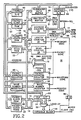
- a control communications interface system 12 serves to provide control access between various modules within the instrument, including the arbitrary waveform generator.
- the communications interface system 12 interacts with a trigger interface system 14, an arbitrary waveform generator (AWG) logic circuit 16, and a waveform memory and multiplexer system 18.
- the trigger interface system 14 receives triggers from and transmits run commands to the AWG logic circuit 16.
- the AWG logic circuit 16 generates address commands for the memory portion of the waveform memory and multiplexer system 18, as well as providing a clock signal for the multiplexer portion.
- a direct memory access (DMA) controller 20 also interacts with the AWG logic circuit 16 and the waveform memory and multiplexer system 18 to load waveform data into the memory portion of the waveform memory and multiplexer system, and to load packet data into the AWG logic circuit, which data defines a desired arbitrary waveform to be generated.
- the DMA controller 20 is accessed via an appropriate interface.
- the waveform memory and multiplexer system 18 provides digitized waveform data to a digital to analog converter (DAC) according to the addresses received from the AWG logic circuit 16 to produce the desired analog waveforms and provides the clock signal to the remainder of the instrument, including the DAC.
- DAC digital to analog converter
- the AWG logic circuit 16 has a plurality of memory devices, such as random access memories (RAM), that contain various elements of a packet data word.
- Each packet data word defines a segment of the desired arbitrary waveform to be generated.
- the elements of the packet data word may include a starting address in the waveform memory, an ending address or length of the waveform segment being defined, a repetition number, and now a duration or clock frequency for the waveform segment.
- the AWG logic circuit 16 is connected to the communications interface system 12 by a communications bus 13, and to the DMA controller system 20 by DMA address and data buses 19, 21 respectively.
- the array of memory devices include a separate memory device for each packet data word element.
- the start address data is stored in a packet start address RAM 22, the length data is stored in a packet length RAM 24, the scan data is stored in a packet scan RAM 26, and the clock data is stored in two packet clock RAMs 28, 30.
- the packet data words may be stored sequentially in the RAMs for a desired waveform, or may be stored randomly.
- the memory devices are addressed via a packet address bus 23, and data is transferred to and from the memory devices via a packet data bus 25.
- the DMA controller system 20 addresses the packet data word RAMs via the DMA address bus 19 over the packet address bus 23, and loads the packet data words in the RAMs via the DMA data bus 21 through a DMA data buffer 32 onto the packet data bus 25. Also connected to the packet data bus 25 are an address counter 34, a packet length counter 36 and a packet scan counter 38.
- a communications data buffer 40 is connected between the communications bus 13 and the packet data bus 25 to transfer data between the communications interface system 12 and the packet data word RAMs. Also connected to the communications bus 13 are a packet address register 40 and a wave number register 42 to receive information at the start of each waveform generation cycle, which information identifies the starting packet address and the number of iterations desired for the resulting generated waveform.
- the information from the packet address and wave number registers 40, 42 are transferred to respective counters 44, 46.
- the wave number counter 46 also is connected to the communications bus 13 to provide feedback to the communications 12 of the status of the waveform generation.
- the output of the packet address counter 44 is coupled through a packet multiplexer 48, to which also is input the address from the DMA address bus 19, to the packet address bus 23 so that the packet RAMs are either addressed by the DMA controller 20 for loading the packets, or by the packet address counter 44 for generating the waveform.
- the particular implementation shown addresses the packet RAMs sequentially, but by appropriate accessing by the communications interface system 12 the packet RAMs may be addressed randomly to generate the desired waveform.
- a clock interface circuit 50 is connected to the communications bus 13 so that a variable clock 54, such as that used for timing and skew in the LT-1000 VLSI Logic Test System manufactured by Tektronix, Inc. of Beaverton, Oregon, may be controlled directly from the communications interface system 12.
- the output of the clock interface circuit 50 as well as the output from the packet clock RAMs 28, 30 are input to a clock multiplexer 52 so that for functions other than arbitrary waveform generation the communications interface system 12 controls the variable clock frequency, and for waveform generation the packet data word controls the variable clock frequency.
- the output of the variable clock 54 is the clock signal that is applied to the multiplexers of the waveform memory and multiplexer system 18 as well as to the remainder of the instrument, and is also applied via an optional divider circuit 56 to the clock inputs of the packet address and length counters 34, 36.
- the output of the packet address counter 34 is applied, together with addresses from the DMA address bus 19, to an address multiplexer 58 to address the memory portion of the waveform memory and multiplexer system 18 in order to load the appropriate waveform segments into the memory from the DMA controller system 20 or to output the addressed waveform segments to the DAC according to the packet address function.
- a packet address readback circuit 60 and an address counter readback circuit 62 are provided between the packet address bus 23 and the communications bus 13 and between the output of the packet address counter 34 and the communications bus to provide feedback to the communications interface system 12.
- the communications interface system 12 loads a starting packet address into the packet address register 40, and a number representing the number of iterations desired for the resulting generated waveform into the wave number register 42.
- the contents of the registers 40, 42 are transferred to their respective counters 44, 46, and the first packet address is applied to the packet address bus 23.
- the contents of the addressed packet data word is transferred into the respective counters 34, 36, 38, and the variable clock control word is applied via the clock multiplexer 52 from the packet clock RAMs 28, 30 to the variable clock 54.
- the start address from the packet address counter 34 is applied to the waveform memory and multiplexer system 18 via the address multiplexer 58 to access the first data point for the desired waveform from the memory portion for transmission to the DAC.
- the packet address counter 34 For each clock pulse from the variable clock 54 the packet address counter 34 is incremented and the packet length counter 36 is effectively decremented. When the length counter 36 overflows, indicating that the waveform segment represented by that packet data word is complete, the packet scan counter 38 is effectively decremented, and the start address from the packet address RAM 22 and the length from the packet length RAM 24 are reloaded into the packet address and length counters 34, 36 to repeat the waveform segment represented by that packet data word.
- the packet address counter 44 When the packet scan counter 38 overflows, indicating that the repetition of that packet data word is completed, the packet address counter 44 is incremented to access the next packet data word for the desired waveform, and the process is repeated as described above.
- an overflow from the packet address counter 44 effectively decrements the wave number counter 46
- the packet address counter 44 is reloaded from the packet address register 40, and the waveform is generated again as described above.
- an overflow from the wave number counter 46 indicates that the process has been completed, and the cormunications interface system 12 then sequences to the next module to continue the testing by the instrument.
- the desired test waveform is a variable frequency sine wave having ten cycles of a sine wave segment at each of ten frequencies, each sine wave segment being twenty data points in length.
- the packet data words loaded into the packet RAMs 22, 24, 26, 28, 30 by the DMA controller system 20 would have a start address corresponding to the memory address in the waveform memory and multiplexer system 18 at which the twenty point sine wave segment begins.
- the length would be twenty to obtain the complete sine wave, and the scan value would be ten since that is the number of cycles of the sine wave desired at each frequency.
- the clock control word would have a value that would cause the variable clock 54 to operate at the desired frequency for that frequency segment of the desired waveform.
- the communications interface system 12 then loads a starting packet address into the packet address register 40 and an iteration number into the wave number register 42, which values are subsequently transferred to the respective counters 44, 46 when the waveform generation starts.
- the first addressed data packet then is processed to produce the first sine wave at a first frequency, and is repeated ten times, and then the packet address is incremented and the next packet data word is executed to produce another ten cycles of the sine wave at a second frequency.
- a complete waveform having a plurality of ten cycle sine waves at different frequencies is produced.
- This complete waveform is repeated ten times according to the waveform iteration number in the waveform number counter 46, and then the arbitrary waveform generation is terminated until a new sequence of packet data words is loaded from the DMA controller system 20 and accessed by the communications interface system 12, or the communications interface system again accesses the current sequence of packet data words.
- the present invention provides an arbitrary waveform generator with adjustable spacing for each segment of a generated waveform by using a control word in a packet data word that determines the frequency of a variable clock, and therefore the duration for each waveform segment represented by the corresponding packet data word.
Landscapes
- Engineering & Computer Science (AREA)
- Theoretical Computer Science (AREA)
- Physics & Mathematics (AREA)
- General Engineering & Computer Science (AREA)
- General Physics & Mathematics (AREA)
- Tests Of Electronic Circuits (AREA)
- Data Exchanges In Wide-Area Networks (AREA)
Applications Claiming Priority (2)
| Application Number | Priority Date | Filing Date | Title |
|---|---|---|---|
| US07/389,076 US4956798A (en) | 1989-08-03 | 1989-08-03 | Arbitrary waveform generator with adjustable spacing |
| US389076 | 1989-08-03 |
Publications (2)
| Publication Number | Publication Date |
|---|---|
| EP0411764A2 true EP0411764A2 (fr) | 1991-02-06 |
| EP0411764A3 EP0411764A3 (en) | 1992-06-03 |
Family
ID=23536712
Family Applications (1)
| Application Number | Title | Priority Date | Filing Date |
|---|---|---|---|
| EP19900307041 Withdrawn EP0411764A3 (en) | 1989-08-03 | 1990-06-27 | Arbitrary waveform generator with adjustable spacing |
Country Status (3)
| Country | Link |
|---|---|
| US (1) | US4956798A (fr) |
| EP (1) | EP0411764A3 (fr) |
| JP (1) | JPH0368204A (fr) |
Cited By (1)
| Publication number | Priority date | Publication date | Assignee | Title |
|---|---|---|---|---|
| EP0543186A1 (fr) * | 1991-11-21 | 1993-05-26 | Sony/Tektronix Corporation | Méthode de génération d'un signal à fréquence variable |
Families Citing this family (16)
| Publication number | Priority date | Publication date | Assignee | Title |
|---|---|---|---|---|
| EP0486851A3 (en) * | 1990-11-19 | 1993-04-07 | Tektronix Inc. | Direct digital synthesizer with feedback shift register |
| US6038578A (en) * | 1990-11-21 | 2000-03-14 | Fogg; Harold T. | Method and system for generating a series of waveform definitions |
| US5734877A (en) * | 1992-09-09 | 1998-03-31 | Silicon Graphics, Inc. | Processor chip having on-chip circuitry for generating a programmable external clock signal and for controlling data patterns |
| US6396801B1 (en) | 1998-03-17 | 2002-05-28 | Trw Inc. | Arbitrary waveform modem |
| US6031479A (en) * | 1998-04-24 | 2000-02-29 | Credence Systems Corproation | Programmable digitizer with adjustable sampling rate and triggering modes |
| US6397173B1 (en) * | 1999-05-03 | 2002-05-28 | Astec International Llc | Application specific waveform generator |
| JP4177744B2 (ja) * | 2003-10-31 | 2008-11-05 | リーダー電子株式会社 | 多相信号発生の方法および装置 |
| US7340357B2 (en) * | 2005-05-27 | 2008-03-04 | National Instruments Corporation | Arbitrary waveform generator with configurable digital signal processing unit |
| JP2009505302A (ja) * | 2005-08-22 | 2009-02-05 | エヌエックスピー ビー ヴィ | マイクロコントローラによる波形発生方法及び装置 |
| US20070067123A1 (en) * | 2005-09-19 | 2007-03-22 | Jungerman Roger L | Advanced arbitrary waveform generator |
| US7714623B2 (en) * | 2008-04-09 | 2010-05-11 | Ut-Battelle, Llc | Agile high resolution arbitrary waveform generator with jitterless frequency stepping |
| WO2012088130A2 (fr) * | 2010-12-23 | 2012-06-28 | Marvell World Trade Ltd. | Représentation ou génération de formes d'ondes arbitraires à faible utilisation de mémoire |
| US8575983B1 (en) | 2012-07-27 | 2013-11-05 | Tektronix, Inc. | Waveform generation circuit for a waveform generator |
| ITBO20130068A1 (it) * | 2013-02-18 | 2014-08-19 | Active Technologies S R L | Metodo e sistema per la sintesi digitale di una forma d'onda |
| CN107436618B (zh) | 2017-08-08 | 2019-12-27 | 电子科技大学 | 一种基于指令架构的任意波形发生器 |
| KR102322147B1 (ko) * | 2019-07-18 | 2021-11-04 | (주)인피니어 | 3상 정현파 생성장치 |
Family Cites Families (4)
| Publication number | Priority date | Publication date | Assignee | Title |
|---|---|---|---|---|
| US4791384A (en) * | 1984-02-15 | 1988-12-13 | Harris Corporation | Programmable function controller for use in a waveform generator system |
| JPS6089226A (ja) * | 1984-03-19 | 1985-05-20 | Namuko:Kk | 任意波形発生回路 |
| US4719593A (en) * | 1984-07-09 | 1988-01-12 | Advanced Micro Devices, Inc. | Apparatus for generating digital timing waveforms |
| US4669024A (en) * | 1985-10-23 | 1987-05-26 | Westinghouse Electric Corp. | Multiphase frequency selective phase locked loop with multiphase sinusoidal and digital outputs |
-
1989
- 1989-08-03 US US07/389,076 patent/US4956798A/en not_active Expired - Fee Related
-
1990
- 1990-06-27 EP EP19900307041 patent/EP0411764A3/en not_active Withdrawn
- 1990-07-30 JP JP2202358A patent/JPH0368204A/ja active Pending
Cited By (1)
| Publication number | Priority date | Publication date | Assignee | Title |
|---|---|---|---|---|
| EP0543186A1 (fr) * | 1991-11-21 | 1993-05-26 | Sony/Tektronix Corporation | Méthode de génération d'un signal à fréquence variable |
Also Published As
| Publication number | Publication date |
|---|---|
| JPH0368204A (ja) | 1991-03-25 |
| US4956798A (en) | 1990-09-11 |
| EP0411764A3 (en) | 1992-06-03 |
Similar Documents
| Publication | Publication Date | Title |
|---|---|---|
| US4956798A (en) | Arbitrary waveform generator with adjustable spacing | |
| US4675546A (en) | Edge programmable timing signal generator | |
| US5589788A (en) | Timing adjustment circuit | |
| US5381421A (en) | Per pin circuit test system having N-bit pin interface providing speed improvement with frequency multiplexing | |
| US5122800A (en) | Variable successive approximation converter | |
| US5682390A (en) | Pattern generator in semiconductor test system | |
| US5521512A (en) | Time domain reflectometer using successively delayed test pulses and an interleaved sampling procedure | |
| JPS5920105B2 (ja) | 波形記憶装置 | |
| US5016226A (en) | Apparatus for generating a data stream | |
| US4586181A (en) | Test pattern generating apparatus | |
| JPWO1999040450A1 (ja) | 半導体デバイス試験装置 | |
| US4222514A (en) | Digital tester | |
| US4855681A (en) | Timing generator for generating a multiplicty of timing signals having selectable pulse positions | |
| JP3710069B2 (ja) | 高速ディジタル/アナログ変換、デシメーションおよび記憶システム並びに方法 | |
| EP0228332B1 (fr) | Système automatique de test ayant une architecture à "vrai testeur-par-broche" | |
| US4864160A (en) | Timing signal generator | |
| JP6301079B2 (ja) | 波形生成回路及び波形生成シーケンス制御方法 | |
| US4737792A (en) | Counter-based simulated target generator | |
| US3822380A (en) | Digitally controlled signal generator | |
| US4845726A (en) | Maximum length linearly recurring sequence generator control device | |
| EP0004152A1 (fr) | Conversion digitale d'un signal analogique périodique | |
| KR100492231B1 (ko) | 자동시험장치(ate)테스터의아날로그채널에서의펄스발생 | |
| US4757465A (en) | Digital interpolator for selectively providing linear interpolation between successive digital data words | |
| US5185874A (en) | Address generator for high speed data averager | |
| JP3488315B2 (ja) | 波形発生装置 |
Legal Events
| Date | Code | Title | Description |
|---|---|---|---|
| PUAI | Public reference made under article 153(3) epc to a published international application that has entered the european phase |
Free format text: ORIGINAL CODE: 0009012 |
|
| AK | Designated contracting states |
Kind code of ref document: A2 Designated state(s): DE FR GB |
|
| PUAL | Search report despatched |
Free format text: ORIGINAL CODE: 0009013 |
|
| AK | Designated contracting states |
Kind code of ref document: A3 Designated state(s): DE FR GB |
|
| 17P | Request for examination filed |
Effective date: 19921102 |
|
| RAP1 | Party data changed (applicant data changed or rights of an application transferred) |
Owner name: CREDENCE SYSTEMS CORPORATION |
|
| STAA | Information on the status of an ep patent application or granted ep patent |
Free format text: STATUS: THE APPLICATION IS DEEMED TO BE WITHDRAWN |
|
| 18D | Application deemed to be withdrawn |
Effective date: 19950103 |