EP0412007B1 - Verfahren zur Herstellung eines dünnen supraleitenden Films - Google Patents
Verfahren zur Herstellung eines dünnen supraleitenden Films Download PDFInfo
- Publication number
- EP0412007B1 EP0412007B1 EP90402197A EP90402197A EP0412007B1 EP 0412007 B1 EP0412007 B1 EP 0412007B1 EP 90402197 A EP90402197 A EP 90402197A EP 90402197 A EP90402197 A EP 90402197A EP 0412007 B1 EP0412007 B1 EP 0412007B1
- Authority
- EP
- European Patent Office
- Prior art keywords
- set forth
- process set
- oxide
- substrate
- range
- Prior art date
- Legal status (The legal status is an assumption and is not a legal conclusion. Google has not performed a legal analysis and makes no representation as to the accuracy of the status listed.)
- Expired - Lifetime
Links
- 239000010409 thin film Substances 0.000 title claims description 33
- 238000004519 manufacturing process Methods 0.000 title claims description 5
- 238000000034 method Methods 0.000 claims description 40
- 239000000758 substrate Substances 0.000 claims description 26
- 150000001875 compounds Chemical class 0.000 claims description 17
- QVGXLLKOCUKJST-UHFFFAOYSA-N atomic oxygen Chemical compound [O] QVGXLLKOCUKJST-UHFFFAOYSA-N 0.000 claims description 15
- 239000007789 gas Substances 0.000 claims description 15
- 239000001301 oxygen Substances 0.000 claims description 15
- 229910052760 oxygen Inorganic materials 0.000 claims description 15
- 238000001451 molecular beam epitaxy Methods 0.000 claims description 14
- 238000001771 vacuum deposition Methods 0.000 claims description 8
- 239000013078 crystal Substances 0.000 claims description 7
- 239000000203 mixture Substances 0.000 claims description 6
- 238000000151 deposition Methods 0.000 claims description 3
- 229910052684 Cerium Inorganic materials 0.000 claims description 2
- 229910052692 Dysprosium Inorganic materials 0.000 claims description 2
- 229910052691 Erbium Inorganic materials 0.000 claims description 2
- 229910052693 Europium Inorganic materials 0.000 claims description 2
- 229910052688 Gadolinium Inorganic materials 0.000 claims description 2
- 229910052689 Holmium Inorganic materials 0.000 claims description 2
- 229910002244 LaAlO3 Inorganic materials 0.000 claims description 2
- 229910002331 LaGaO3 Inorganic materials 0.000 claims description 2
- 229910052765 Lutetium Inorganic materials 0.000 claims description 2
- 229910003200 NdGaO3 Inorganic materials 0.000 claims description 2
- 229910052779 Neodymium Inorganic materials 0.000 claims description 2
- 229910052777 Praseodymium Inorganic materials 0.000 claims description 2
- 229910052772 Samarium Inorganic materials 0.000 claims description 2
- 229910002370 SrTiO3 Inorganic materials 0.000 claims description 2
- 229910052771 Terbium Inorganic materials 0.000 claims description 2
- 229910052775 Thulium Inorganic materials 0.000 claims description 2
- 229910052769 Ytterbium Inorganic materials 0.000 claims description 2
- 229910052746 lanthanum Inorganic materials 0.000 claims description 2
- CPLXHLVBOLITMK-UHFFFAOYSA-N magnesium oxide Inorganic materials [Mg]=O CPLXHLVBOLITMK-UHFFFAOYSA-N 0.000 claims description 2
- 229910001233 yttria-stabilized zirconia Inorganic materials 0.000 claims description 2
- 229910052727 yttrium Inorganic materials 0.000 claims description 2
- 230000008021 deposition Effects 0.000 claims 1
- MYMOFIZGZYHOMD-UHFFFAOYSA-N Dioxygen Chemical compound O=O MYMOFIZGZYHOMD-UHFFFAOYSA-N 0.000 description 6
- 229910001882 dioxygen Inorganic materials 0.000 description 5
- 239000012495 reaction gas Substances 0.000 description 5
- 239000002887 superconductor Substances 0.000 description 5
- 230000015572 biosynthetic process Effects 0.000 description 4
- 239000010408 film Substances 0.000 description 3
- 150000002926 oxygen Chemical class 0.000 description 2
- 238000007738 vacuum evaporation Methods 0.000 description 2
- ATJFFYVFTNAWJD-UHFFFAOYSA-N Tin Chemical compound [Sn] ATJFFYVFTNAWJD-UHFFFAOYSA-N 0.000 description 1
- 229910052797 bismuth Inorganic materials 0.000 description 1
- JCXGWMGPZLAOME-UHFFFAOYSA-N bismuth atom Chemical compound [Bi] JCXGWMGPZLAOME-UHFFFAOYSA-N 0.000 description 1
- 239000000470 constituent Substances 0.000 description 1
- 238000001704 evaporation Methods 0.000 description 1
- 230000005283 ground state Effects 0.000 description 1
- 238000010438 heat treatment Methods 0.000 description 1
- 238000007733 ion plating Methods 0.000 description 1
- 239000000463 material Substances 0.000 description 1
- 238000002360 preparation method Methods 0.000 description 1
- 230000005855 radiation Effects 0.000 description 1
- 239000004065 semiconductor Substances 0.000 description 1
- 229910052710 silicon Inorganic materials 0.000 description 1
- 239000010703 silicon Substances 0.000 description 1
- 238000004544 sputter deposition Methods 0.000 description 1
- 229910021521 yttrium barium copper oxide Inorganic materials 0.000 description 1
Images
Classifications
-
- H—ELECTRICITY
- H10—SEMICONDUCTOR DEVICES; ELECTRIC SOLID-STATE DEVICES NOT OTHERWISE PROVIDED FOR
- H10N—ELECTRIC SOLID-STATE DEVICES NOT OTHERWISE PROVIDED FOR
- H10N60/00—Superconducting devices
- H10N60/01—Manufacture or treatment
- H10N60/0268—Manufacture or treatment of devices comprising copper oxide
- H10N60/0296—Processes for depositing or forming copper oxide superconductor layers
- H10N60/0381—Processes for depositing or forming copper oxide superconductor layers by evaporation, e.g. MBE
Definitions
- the present invention relates to a process for preparing superconducting thin films. More particularly, it relates to a process for depositing a superconducting thin films of compound oxides on substrates by vacuum evaporation techniques such as molecular beam epitaxy (hereinafter MBE) method.
- MBE molecular beam epitaxy
- vacuum evaporation methods are widely used because film formation is realized under very low pressures so that a variety of properties of a thin film can be analyzed advantageously during their growing stage.
- An activated reactive evaporation method is one of techniques to prepare thin films of compounds.
- material vapors which are evaporated in an active gas atmosphere are reacted on a substrate.
- the MBE method is advantageous for preparing thin films of multi-component compounds because of the easiness of control of compositions. In some compounds, these two methods are combined together to prepare their thin films.
- oxygen gas as the active gas
- microwave or other radiations it is known to activate or excite the oxygen gas by microwave or other radiations in order to increase its activity before an oxide thin film is deposited on a substrate.
- p 1660 to 1662 discloses a process for preparing an oxide thin film on a substrate by a vacuum evaporation method (MBE) comprising the introduction of an excited oxygen gas (oxygen plasma) in the neighbourhood of the substrate.
- MBE vacuum evaporation method
- a vacuum chamber of a MBE unit must be evacuated to a pressure below 1,33 10 ⁇ 2Pa (10 ⁇ 4Torr) and hence a plasma generating zone becomes such a low pressure value as several tens Pa (hunderds milli-Torr) to several hunhundreds Pa (Torr).However, it is difficult to produce a stable plasma under such low pressures.
- An object of the present invention is to solve the problems raised by prior art and to provide a process which permits to prepare oxide thin films having predetermined oxygen content and of high quality.
- the present invention provides a process for preparing an oxide thin film on a substrate by a vacuum evaporation method with an oxygen-containing gas excited by microwave discharge being introduced in the neighbourhood of the substrate, characterized in that the oxygen-containing gas is a mixed gas of O2 and N2.
- the process according to the present invention is applicable to formation of any oxide thin films on substrates, it is particularly and advantageously applicable for depositing superconducting thin films of compound oxides whose oxygen content is a critical factor in order to realize superconducting properties.
- Selection of the substrate on which the oxide thin film is formed depends on kinds and applications of the oxide to be deposited.
- the substrate and the oxide thin films can be combined from a wide variety.
- the substrate is preferably made of oxides, more preferably single crystal oxides.
- the preferable single crystal oxides are MgO, SrTiO3, LaGaO3, NdGaO3, LaAlO3 or YSZ.
- a single crystal of semiconductors such as silicon may be used.
- the process according to the present invention can be carried out by any vacuum evaporation technique including vacuum deposition method, sputtering method, ion-plating method or the like, the process according to the present invention is advantageous when superconducting thin films of compound oxide whose oxygen content is critical is prepared by the MBE method in which the control of oxygen supply is difficult.
- constituent elements of an oxide to be deposited are evaporated by means of Kunudsen Cells (K-cells) while activated oxygen gas, as a reaction gas, is supplied in the neighbourhood of a surface of the substrate.
- K-cells Kunudsen Cells
- activated oxygen gas as a reaction gas
- the present invention resides in that a mixed gas of O2 and N2 which is excited by microwave is supplied in the neighbourhood of a substrate at the same time as a thin film of oxide is deposited by a vacuum evaporation method, particularly by the MBE method.
- the process according to the present invention is particularly effective for preparation of thin films of oxide superconductors which are very sensitive to the oxygen contents.
- a proportion of N2 is preferably in a range of 5 to 80 % by volume. If the proportion of N2 is less than 5 %, substantially no advantage of the present invention over the prior arts in which oxygen alone is used will be obtained. To the contrary, if the proportion of N2 exceeds 80 %, a proportion of O2 becomes too small to contribute actual reaction and the properties of the thin film obtained are rather deteriorated.
- the flow rate of the mixed gas of O2 and N2 depends on the power of an evacuation system used but is preferably in a range of 0.1 to 50 cc/min.
- the process according to the present invention can be performed very easily by replacing oxygen gas which was used as a reaction gas in the prior art by the mixed gas of O2 and N2 , with substantially no change of the conventional film formation unit.
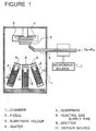
- FIG. 1 is an illustrative view of a MBE unit for carrying out the process according to the present invention.
- the process according to the present invention can be carried out in the MBE unit shown in Fig. 1.
- the MBE unit shown in Fig. 1 comprises a chamber 1 interior of which is evacuated to very high vacuum, a plurality of Kunudsen Cells (K-cells) 2 each of which can control a temperature of a vapour source 10 placed therein, a plurality of shutters 8 for controlling the amount or timing of each vapour source 10, a substrate holder 3 provided with a heater 4 for heating a substrate 5, and a reaction gas supply pipe 6 through which a reaction gas is supplied and being opened in the neighbourhood of a surface of the substrate 5.
- the reaction gas is excited by microwave discharge generated by a microwave source 7.
- a superconducting thin film of compound oxide according to the present invention of Y1 Ba2 Cu3 O 7-x was deposited on a ⁇ 100 ⁇ plane of a MgO single crystal substrate by the molecular beam epitaxy (MBE) unit illustrated in Fig. 1, with supplying a gas mixture of O2 and N2 according to the present invention.
- MBE molecular beam epitaxy
Landscapes
- Engineering & Computer Science (AREA)
- Manufacturing & Machinery (AREA)
- Inorganic Compounds Of Heavy Metals (AREA)
- Superconductors And Manufacturing Methods Therefor (AREA)
- Oxygen, Ozone, And Oxides In General (AREA)
- Crystals, And After-Treatments Of Crystals (AREA)
- Physical Vapour Deposition (AREA)
- Superconductor Devices And Manufacturing Methods Thereof (AREA)
- Inorganic Insulating Materials (AREA)
Claims (15)
- Verfahren zur Herstellung eines dünnen Oxidfilms auf einem Substrat (5) durch ein Vakuumverdampfungsverfahren, bei dem ein durch eine Mikrowellenentladung (7) angeregtes sauerstoffhaltiges Gas in der Nähe des Substrats eingeführt wird, dadurch gekennzeichnet, daß das sauerstoffhaltige Gas ein Gasgemisch aus O₂ und N₂ ist.
- Verfahren nach Anspruch 1, bei dem das Vakuumverdampfungsverfahren eine Molekularstrahlepitaxie (MBE) ist.
- Verfahren nach Anspruch 1 oder 2, bei dem die Durchflußgeschwindigkeit des sauerstoffhaltigen Gases im Bereich von 0,1 bis 50 cc/min liegt.
- Verfahren nach einem der Ansprüche 1 bis 3, bei dem der Anteil an N₂ zwischen 5 und 80 Volumen-% beträgt.
- Verfahren nach einem der Ansprüche 1 bis 4, bei dem der Druck in der Vakuumkammer im Bereich von 1,33 x 10⁻⁴ bis 1,33 x 10⁻² Pa liegt (1,0 x 10⁻⁶ bis 1,0 x 10⁻⁴ Torr).
- Verfahren nach einem der Ansprüche 1 bis 5, bei dem die Abscheiderate im Bereich von 10⁻¹¹ bis 10⁻⁹ m/sec (0,1 bis 10 Å/sec) liegt.
- Verfahren nach einem der Ansprüche 1 bis 6, bei dem die Substrattemperatur im Bereich von 550 bis 800° C liegt.
- Verfahren nach einem der Ansprüche 1 bis 7, bei dem die Leistung der Mikrowelle zur Gasanregung im Bereich von 50 bis 500 W liegt.
- Verfahren nach einem der Ansprüche 1 bis 8, bei dem das Substrat ein Oxid-Einkristall ist.
- Verfahren nach Anspruch 9, bei dem das Substrat ein Oxid-Einkristall ist ausgewählt aus der Gruppe umfassend MgO, SrTiO₃, LaGaO₃, NdGaO₃, LaAlO₃ und YSZ.
- Verfahren nach einem der Ansprüche 1 bis 10, bei dem der dünne Oxidfilm ein supraleitender dünner Film aus Verbundoxid ist.
- Verfahren nach Anspruch 11, bei dem das Verbundoxid eine Zusammensetzung aufweist die durch die folgende allgemeine Formel gegeben ist:

- Verfahren nach Anspruch 11, bei dem das Verbundoxid eine Zusammensetzung aufweist die durch die folgende allgemeine Formel gegeben ist:

- Verfahren nach Anspruch 13, bei dem das Verbundoxid eine Kristallstruktur vom Perovskit-Typ oder geschichteten Perovskit-Typ aufweist.
- Verfahren nach Anspruch 11, bei dem das Verbundoxid eine Zusammensetzung aufweist die durch die folgende allgemeine Formel gegeben ist:

Applications Claiming Priority (2)
| Application Number | Priority Date | Filing Date | Title |
|---|---|---|---|
| JP1198647A JPH0365501A (ja) | 1989-07-31 | 1989-07-31 | 酸化物薄膜の作製方法 |
| JP198647/89 | 1989-07-31 |
Publications (3)
| Publication Number | Publication Date |
|---|---|
| EP0412007A2 EP0412007A2 (de) | 1991-02-06 |
| EP0412007A3 EP0412007A3 (en) | 1991-04-10 |
| EP0412007B1 true EP0412007B1 (de) | 1994-12-07 |
Family
ID=16394694
Family Applications (1)
| Application Number | Title | Priority Date | Filing Date |
|---|---|---|---|
| EP90402197A Expired - Lifetime EP0412007B1 (de) | 1989-07-31 | 1990-07-31 | Verfahren zur Herstellung eines dünnen supraleitenden Films |
Country Status (5)
| Country | Link |
|---|---|
| EP (1) | EP0412007B1 (de) |
| JP (1) | JPH0365501A (de) |
| CA (1) | CA2022358C (de) |
| DE (1) | DE69014758T2 (de) |
| HK (1) | HK164795A (de) |
Families Citing this family (3)
| Publication number | Priority date | Publication date | Assignee | Title |
|---|---|---|---|---|
| US5342826A (en) * | 1991-10-02 | 1994-08-30 | International Superconductivity Technology Center | Bi-Sr-Ca-Cu-O superconducting thin film |
| CA2093729C (en) | 1992-04-10 | 2001-01-02 | Takao Nakamura | Process for preparing superconducting thin film formed of oxide superconductor material |
| KR100396251B1 (ko) * | 2001-05-04 | 2003-09-02 | 이만택 | 모발처리용 로트 |
Family Cites Families (3)
| Publication number | Priority date | Publication date | Assignee | Title |
|---|---|---|---|---|
| JPH0817253B2 (ja) * | 1987-09-16 | 1996-02-21 | 株式会社半導体エネルギー研究所 | 酸化物超伝導膜形成方法 |
| JPH01104763A (ja) * | 1987-10-16 | 1989-04-21 | Canon Inc | 金属化合物薄膜の製造方法 |
| JPH0829943B2 (ja) * | 1988-05-13 | 1996-03-27 | 沖電気工業株式会社 | 超伝導体薄膜の形成方法 |
-
1989
- 1989-07-31 JP JP1198647A patent/JPH0365501A/ja active Pending
-
1990
- 1990-07-31 DE DE69014758T patent/DE69014758T2/de not_active Expired - Fee Related
- 1990-07-31 CA CA002022358A patent/CA2022358C/en not_active Expired - Fee Related
- 1990-07-31 EP EP90402197A patent/EP0412007B1/de not_active Expired - Lifetime
-
1995
- 1995-10-19 HK HK164795A patent/HK164795A/en not_active IP Right Cessation
Also Published As
| Publication number | Publication date |
|---|---|
| JPH0365501A (ja) | 1991-03-20 |
| DE69014758D1 (de) | 1995-01-19 |
| CA2022358C (en) | 1998-10-06 |
| EP0412007A2 (de) | 1991-02-06 |
| HK164795A (en) | 1995-10-27 |
| EP0412007A3 (en) | 1991-04-10 |
| DE69014758T2 (de) | 1995-06-22 |
| CA2022358A1 (en) | 1991-02-01 |
Similar Documents
| Publication | Publication Date | Title |
|---|---|---|
| US5039657A (en) | Preparation of superconducting oxide films by reactive evaporation using ozone | |
| US5447908A (en) | Superconducting thin film and a method for preparing the same | |
| US4950642A (en) | Method for fabricating superconducting oxide thin films by activated reactive evaporation | |
| US5252547A (en) | Method of forming an inorganic protective layer on an oxide superconducting film | |
| US5712227A (en) | Substrate having a superconductor layer | |
| US5350737A (en) | MBE process for preparing oxide superconducting films | |
| EP0292958B1 (de) | Verfahren zur Herstellung einer dünnen Schicht aus supraleitendem Mischoxid | |
| US4988670A (en) | Method of forming oxide superconducting films by in-situ annealing | |
| US5057201A (en) | Process for depositing a superconducting thin film | |
| EP0362000B1 (de) | Verfahren zum Herstellen eines Oxid-Supraleiters vom Bismut-Typ | |
| Nakayama et al. | Superconductivity of Bi2Sr2Ca n− 1Cu n O y (n= 2, 3, 4, and 5) thin films prepared in situ by molecular‐beam epitaxy technique | |
| EP0305292B1 (de) | Verfahren zur Herstellung einer dünnen Schicht aus zusammengesetztem supraleitendem Oxyd | |
| EP0410868A2 (de) | Supraleitende Dünnschicht aus Oxid und Verfahren zu deren Herstellung | |
| HK164795A (en) | Process for preparing superconducting thin films | |
| EP0347336B1 (de) | Verfahren zur Abscheidung einer dünnen Supraleiterschicht | |
| US5061684A (en) | Production of thin layers of a high temperature superconductor (htsc) by a plasma-activated physical vapor deposition process, and cathodes used therein | |
| AU614656B2 (en) | Improvement in a process for producing thallium type superconducting thin film | |
| US5478800A (en) | Process for preparing a superconducting thin film | |
| EP0412000B1 (de) | Verfahren zur Herstellung von supraleitenden Dünnschichten | |
| EP0624910B1 (de) | Verfahren zur Herstellung einer supraleitenden dünnen Schicht vom Hg-Typ | |
| US5260267A (en) | Method for forming a Bi-containing superconducting oxide film on a substrate with a buffer layer of Bi2 O3 | |
| US4914080A (en) | Method for fabricating superconductive film | |
| EP0333513B1 (de) | Oxid-Supraleiter | |
| JP2502344B2 (ja) | 複合酸化物超電導体薄膜の作製方法 | |
| JPH05213617A (ja) | 酸化物超伝導体薄膜の形成方法 |
Legal Events
| Date | Code | Title | Description |
|---|---|---|---|
| PUAI | Public reference made under article 153(3) epc to a published international application that has entered the european phase |
Free format text: ORIGINAL CODE: 0009012 |
|
| AK | Designated contracting states |
Kind code of ref document: A2 Designated state(s): DE FR GB |
|
| 17P | Request for examination filed |
Effective date: 19901217 |
|
| PUAL | Search report despatched |
Free format text: ORIGINAL CODE: 0009013 |
|
| AK | Designated contracting states |
Kind code of ref document: A3 Designated state(s): DE FR GB |
|
| 17Q | First examination report despatched |
Effective date: 19930311 |
|
| GRAA | (expected) grant |
Free format text: ORIGINAL CODE: 0009210 |
|
| AK | Designated contracting states |
Kind code of ref document: B1 Designated state(s): DE FR GB |
|
| REF | Corresponds to: |
Ref document number: 69014758 Country of ref document: DE Date of ref document: 19950119 |
|
| ET | Fr: translation filed | ||
| PLBE | No opposition filed within time limit |
Free format text: ORIGINAL CODE: 0009261 |
|
| STAA | Information on the status of an ep patent application or granted ep patent |
Free format text: STATUS: NO OPPOSITION FILED WITHIN TIME LIMIT |
|
| 26N | No opposition filed | ||
| REG | Reference to a national code |
Ref country code: GB Ref legal event code: IF02 |
|
| PGFP | Annual fee paid to national office [announced via postgrant information from national office to epo] |
Ref country code: GB Payment date: 20020731 Year of fee payment: 13 |
|
| PGFP | Annual fee paid to national office [announced via postgrant information from national office to epo] |
Ref country code: DE Payment date: 20020807 Year of fee payment: 13 |
|
| PGFP | Annual fee paid to national office [announced via postgrant information from national office to epo] |
Ref country code: FR Payment date: 20030711 Year of fee payment: 14 |
|
| PG25 | Lapsed in a contracting state [announced via postgrant information from national office to epo] |
Ref country code: GB Free format text: LAPSE BECAUSE OF NON-PAYMENT OF DUE FEES Effective date: 20030731 |
|
| PG25 | Lapsed in a contracting state [announced via postgrant information from national office to epo] |
Ref country code: DE Free format text: LAPSE BECAUSE OF NON-PAYMENT OF DUE FEES Effective date: 20040203 |
|
| GBPC | Gb: european patent ceased through non-payment of renewal fee |
Effective date: 20030731 |
|
| PG25 | Lapsed in a contracting state [announced via postgrant information from national office to epo] |
Ref country code: FR Free format text: LAPSE BECAUSE OF NON-PAYMENT OF DUE FEES Effective date: 20050331 |
|
| REG | Reference to a national code |
Ref country code: FR Ref legal event code: ST |