EP0412036A2 - Correction de positionnement d'éléments d'image dans la plage de balayage d'un système de balayage à laser à faisceaux multiples - Google Patents
Correction de positionnement d'éléments d'image dans la plage de balayage d'un système de balayage à laser à faisceaux multiples Download PDFInfo
- Publication number
- EP0412036A2 EP0412036A2 EP90480085A EP90480085A EP0412036A2 EP 0412036 A2 EP0412036 A2 EP 0412036A2 EP 90480085 A EP90480085 A EP 90480085A EP 90480085 A EP90480085 A EP 90480085A EP 0412036 A2 EP0412036 A2 EP 0412036A2
- Authority
- EP
- European Patent Office
- Prior art keywords
- pulse
- laser
- reference beam
- pulses
- steps
- Prior art date
- Legal status (The legal status is an assumption and is not a legal conclusion. Google has not performed a legal analysis and makes no representation as to the accuracy of the status listed.)
- Granted
Links
Images



Classifications
-
- G—PHYSICS
- G06—COMPUTING OR CALCULATING; COUNTING
- G06K—GRAPHICAL DATA READING; PRESENTATION OF DATA; RECORD CARRIERS; HANDLING RECORD CARRIERS
- G06K15/00—Arrangements for producing a permanent visual presentation of the output data, e.g. computer output printers
- G06K15/02—Arrangements for producing a permanent visual presentation of the output data, e.g. computer output printers using printers
- G06K15/12—Arrangements for producing a permanent visual presentation of the output data, e.g. computer output printers using printers by photographic printing, e.g. by laser printers
- G06K15/1238—Arrangements for producing a permanent visual presentation of the output data, e.g. computer output printers using printers by photographic printing, e.g. by laser printers simultaneously exposing more than one point
- G06K15/1257—Arrangements for producing a permanent visual presentation of the output data, e.g. computer output printers using printers by photographic printing, e.g. by laser printers simultaneously exposing more than one point on more than one main scanning line
- G06K15/1261—Arrangements for producing a permanent visual presentation of the output data, e.g. computer output printers using printers by photographic printing, e.g. by laser printers simultaneously exposing more than one point on more than one main scanning line using an array of light sources
-
- H—ELECTRICITY
- H04—ELECTRIC COMMUNICATION TECHNIQUE
- H04N—PICTORIAL COMMUNICATION, e.g. TELEVISION
- H04N1/00—Scanning, transmission or reproduction of documents or the like, e.g. facsimile transmission; Details thereof
- H04N1/04—Scanning arrangements, i.e. arrangements for the displacement of active reading or reproducing elements relative to the original or reproducing medium, or vice versa
- H04N1/047—Detection, control or error compensation of scanning velocity or position
- H04N1/053—Detection, control or error compensation of scanning velocity or position in main scanning direction, e.g. synchronisation of line start or picture elements in a line
-
- H—ELECTRICITY
- H04—ELECTRIC COMMUNICATION TECHNIQUE
- H04N—PICTORIAL COMMUNICATION, e.g. TELEVISION
- H04N1/00—Scanning, transmission or reproduction of documents or the like, e.g. facsimile transmission; Details thereof
- H04N1/04—Scanning arrangements, i.e. arrangements for the displacement of active reading or reproducing elements relative to the original or reproducing medium, or vice versa
- H04N1/19—Scanning arrangements, i.e. arrangements for the displacement of active reading or reproducing elements relative to the original or reproducing medium, or vice versa using multi-element arrays
- H04N1/191—Scanning arrangements, i.e. arrangements for the displacement of active reading or reproducing elements relative to the original or reproducing medium, or vice versa using multi-element arrays the array comprising a one-dimensional [1D] array
- H04N1/1911—Simultaneously or substantially simultaneously scanning picture elements on more than one main scanning line, e.g. scanning in swaths
-
- H—ELECTRICITY
- H04—ELECTRIC COMMUNICATION TECHNIQUE
- H04N—PICTORIAL COMMUNICATION, e.g. TELEVISION
- H04N1/00—Scanning, transmission or reproduction of documents or the like, e.g. facsimile transmission; Details thereof
- H04N1/04—Scanning arrangements, i.e. arrangements for the displacement of active reading or reproducing elements relative to the original or reproducing medium, or vice versa
- H04N1/113—Scanning arrangements, i.e. arrangements for the displacement of active reading or reproducing elements relative to the original or reproducing medium, or vice versa using oscillating or rotating mirrors
- H04N1/1135—Scanning arrangements, i.e. arrangements for the displacement of active reading or reproducing elements relative to the original or reproducing medium, or vice versa using oscillating or rotating mirrors for the main-scan only
-
- H—ELECTRICITY
- H04—ELECTRIC COMMUNICATION TECHNIQUE
- H04N—PICTORIAL COMMUNICATION, e.g. TELEVISION
- H04N1/00—Scanning, transmission or reproduction of documents or the like, e.g. facsimile transmission; Details thereof
- H04N1/04—Scanning arrangements, i.e. arrangements for the displacement of active reading or reproducing elements relative to the original or reproducing medium, or vice versa
- H04N1/12—Scanning arrangements, i.e. arrangements for the displacement of active reading or reproducing elements relative to the original or reproducing medium, or vice versa using the sheet-feed movement or the medium-advance or the drum-rotation movement as the slow scanning component, e.g. arrangements for the main-scanning
-
- H—ELECTRICITY
- H04—ELECTRIC COMMUNICATION TECHNIQUE
- H04N—PICTORIAL COMMUNICATION, e.g. TELEVISION
- H04N2201/00—Indexing scheme relating to scanning, transmission or reproduction of documents or the like, and to details thereof
- H04N2201/024—Indexing scheme relating to scanning, transmission or reproduction of documents or the like, and to details thereof deleted
- H04N2201/02406—Arrangements for positioning elements within a head
- H04N2201/02439—Positioning method
-
- H—ELECTRICITY
- H04—ELECTRIC COMMUNICATION TECHNIQUE
- H04N—PICTORIAL COMMUNICATION, e.g. TELEVISION
- H04N2201/00—Indexing scheme relating to scanning, transmission or reproduction of documents or the like, and to details thereof
- H04N2201/04—Scanning arrangements
- H04N2201/047—Detection, control or error compensation of scanning velocity or position
- H04N2201/04701—Detection of scanning velocity or position
- H04N2201/0471—Detection of scanning velocity or position using dedicated detectors
- H04N2201/04712—Detection of scanning velocity or position using dedicated detectors using unbroken arrays of detectors, i.e. detectors mounted on the same substrate
-
- H—ELECTRICITY
- H04—ELECTRIC COMMUNICATION TECHNIQUE
- H04N—PICTORIAL COMMUNICATION, e.g. TELEVISION
- H04N2201/00—Indexing scheme relating to scanning, transmission or reproduction of documents or the like, and to details thereof
- H04N2201/04—Scanning arrangements
- H04N2201/047—Detection, control or error compensation of scanning velocity or position
- H04N2201/04701—Detection of scanning velocity or position
- H04N2201/04732—Detecting at infrequent intervals, e.g. once or twice per line for main-scan control
-
- H—ELECTRICITY
- H04—ELECTRIC COMMUNICATION TECHNIQUE
- H04N—PICTORIAL COMMUNICATION, e.g. TELEVISION
- H04N2201/00—Indexing scheme relating to scanning, transmission or reproduction of documents or the like, and to details thereof
- H04N2201/04—Scanning arrangements
- H04N2201/047—Detection, control or error compensation of scanning velocity or position
- H04N2201/04701—Detection of scanning velocity or position
- H04N2201/04744—Detection of scanning velocity or position by detecting the scanned beam or a reference beam
-
- H—ELECTRICITY
- H04—ELECTRIC COMMUNICATION TECHNIQUE
- H04N—PICTORIAL COMMUNICATION, e.g. TELEVISION
- H04N2201/00—Indexing scheme relating to scanning, transmission or reproduction of documents or the like, and to details thereof
- H04N2201/04—Scanning arrangements
- H04N2201/047—Detection, control or error compensation of scanning velocity or position
- H04N2201/04753—Control or error compensation of scanning position or velocity
- H04N2201/04758—Control or error compensation of scanning position or velocity by controlling the position of the scanned image area
- H04N2201/04767—Control or error compensation of scanning position or velocity by controlling the position of the scanned image area by controlling the timing of the signals, e.g. by controlling the frequency o phase of the pixel clock
- H04N2201/04781—Controlling the phase of the signals
- H04N2201/04786—Controlling a start time, e.g. for output of a line of data
-
- H—ELECTRICITY
- H04—ELECTRIC COMMUNICATION TECHNIQUE
- H04N—PICTORIAL COMMUNICATION, e.g. TELEVISION
- H04N2201/00—Indexing scheme relating to scanning, transmission or reproduction of documents or the like, and to details thereof
- H04N2201/04—Scanning arrangements
- H04N2201/047—Detection, control or error compensation of scanning velocity or position
- H04N2201/04753—Control or error compensation of scanning position or velocity
- H04N2201/04794—Varying the control or compensation during the scan, e.g. using continuous feedback or from line to line
Definitions
- This invention relates to multiple beam laser scanning systems and more particularly to an electronic correction scheme for correcting pel placement errors due to mechanical misalignments and electrical propagation delays from laser beam to laser beam.
- Multiple beam lasing systems can be used in a variety of applications, one of which is in a printing system where rotating polygonal mirrors are used to scan the light beams across a photoreceptive surface.
- the use of multiple laser beams in a printing system provides the capa bility of producing more than one line of information at a time, thus enabling high pel resolution, for example, 480 pels per inch or higher while keeping practical speeds for the rotating polygonal mirror.
- Multiple beam devices provide other capabilities as well; that is, the multiple beams can be used to alter the shape of the effective writing spot by modulating the spots within the spot group or they can be used to modulate the amount of light provided at each pel position.
- Still another problem with multiple beam lasing systems is variable electrical propagation delays resulting from the use of different laser drivers for each laser source. Even though the drivers are of the same design, the different components comprising the drivers create a variable delay in turning the beams on and off from one laser to another, thus creating pel placement variations. Since these variations can change with the temperature and age of the laser driver, pel placement errors change dynamically.
- Electronic correction schemes in the prior art achieve multiple pel correction for misalignments due to a necessary tilting of a laser array. Some of these electronic schemes provide sub-pel accuracy. Such systems require nanosecond resolution when high resolution systems are contemplated, that is, 480 pels per inch or higher. Clock frequencies of 500 x 106 Hz are required to resolve to two nanoseconds. Such a clock and the high speed logic utilizing such resolution are expensive.
- This invention relates to electronic correction for electrical propagation delays as well as mechanical misalignment problems within a multiple beam laser printhead by providing a closed loop correction system in which control signals are produced from the energization of the laser beams. Energization points are then moved to a desired location and matched, beam to beam. Sub-pel correction is achieved with relatively low clock frequencies through the use of tapped or programmable delay lines.
- the method of correcting pel placement involves sensing the position at which a reference laser beam turns on and then adjusting that position to a desired point. Non-reference laser beams are then turned on, one at a time, and the turn-on point adjusted until it is at the same position as the reference beam. This enables the beams to write pels in alignment from line to line despite the presence of mechanical and electrical skew.
- beams are aligned by sensing the turn-on point at the trailing edge of a sensing element.
- beams are aligned by matching the points of full laser energy, beam to beam, at the junction of the same two elements of a CCD array.
- tapped delay lines or programmable delay lines are used to provide resolution to a sub-pel basis.
- the application of this invention can be illustrated within the framework of electrophotographic machines wherein prints are produced by creating an image of the subject on a photoreceptive surface, developing the image, and then fusing the image to paper or other print receiving material.
- the electrophotographic process is of the transfer type where photoreceptive material is placed around a rotating drum or arranged as a belt to be driven by a system of roll ers.
- photoreceptive material is passed under a stationary charge generating station to place a relatively uniform electrostatic charge, usually several hundred volts, across the entirety of the photoreceptive surface.
- the photoreceptor is moved to an imaging station where it receives light rays from a light generating source which will discharge the photoreceptor to relatively low levels when the light source is fully powered, while the photoreceptor will continue to carry high voltage levels when the light source is turned off, or when it is powered at intermediate levels or for a relatively short duration.
- the photoreceptive material is caused to bear a charge pattern which corresponds to the printing, shading, etc., which is desired to be printed on the receiving material.
- Light generating sources in an electrophotographic printer are frequently comprised of lasing means in which the beam is modulated by a character generator to control the power or the length of time that a beam exposes the photoconductor in a particular pel area.
- character generators may modulate more than one beam at a time, so that more than one line of pels may be written at a time.
- the image After producing an image on the photoreceptor, the image is moved to a developing station in the machine where developing material called toner is placed on the image.
- This material is usually in the form of a powder which carries a charge designed to cause the powder to deposit on selected areas of the photoreceptor.
- the developed image is moved from the developer to a transfer station where the copy receiving material, usual ly paper, is juxtaposed to the developed image and a charge is placed on the backside of the paper so that when it is stripped from the photoreceptor the toner material is held on the paper and removed from the photoreceptor.
- the copy receiving material usual ly paper
- the remaining process steps are for permanently bonding toner material to the copy paper and cleaning residual toner left on the photoreceptor so that it can be reused.
- FIG. 1 shows a typical electrophotographic machine such as would be used to implement this invention.
- Photoreceptive material 10 is placed on the surface of a drum 11 which is driven by motive means, not shown, to rotate in the direction A.
- a charge generator 12 places a uniform charge of several hundred volts across the surface of the photoreceptor at charging station 12′.
- the charged photoreceptor is mounted in a dark enclosure, not shown, and rotates to a printhead 13 which is comprised of a light generating source, such as a multiple beam laser generator.
- the light source selectively exposes the charged photoreceptor at imaging station 13′ to discharge it in areas which are desired to be developed (Discharged Area Development, DAD process), or discharge it in areas which are to remain free of toner (Charged Area Development, CAD process).
- the discharged areas of the photo receptor are developed at developing station 14′ by developer apparatus 14 which applies toner so that the photo receptor carries a visually perceptible image of the data.
- the developed image rotates to transfer station 15′ where print paper, moving in the direction B, is juxtaposed with the surface of the photoreceptor.
- a charge opposite in polarity to the charge on the toner is placed on the backside of the print paper by transfer charge generator 15 such that when the paper is stripped from the surface of the photoreceptor, toner will be attracted to the paper and leave the surface of photoreceptor 10. Any remaining residual toner is cleaned from the photoreceptor at cleaning station 16′ by cleaning apparatus 16.
- the print-head modulator is comprised of a power supply, which will either turn the light source on for longer or shorter periods of time to accomplish varying degrees of photoreceptor discharge in accordance with the pattern data, or it will turn the light-generating source on to a greater or lesser illumination intensity in accordance with that data. In any event, modulation will occur in accordance with that data contained in memory 19. That data is sent to a raster buffer 18 and on to the printhead modulator 17.
- FIG. 2 shows an optical scanning system for use in printhead 13 of the electrophotographic machine shown in FIG. 1.
- four (4) nearly coaxial laser beams 40-43 are shown emanating from a multiple beam laser array module 24.
- the four (4) laser beams 40-43 are passed through a cylindrical lens 25 for focusing each of the beams onto the facets 26 of a rotating polygonal mirror.
- the beams are reflected from the rotating mirror through a negative power spherical lens group 27, anamorphic lens group 28, and a positive power spherical lens group 29, and onto the surface of photoreceptor 10.
- FIG. 1 shows an optical scanning system for use in printhead 13 of the electrophotographic machine shown in FIG. 1.
- four (4) nearly coaxial laser beams 40-43 emanating from a multiple beam laser array module 24.
- the four (4) laser beams 40-43 are passed through a cylindrical lens 25 for focusing each of the beams onto the facets 26 of
- FIG. 2 shows a fold mirror 30, an exit window 31, the length 32 of the scan across photoreceptor 10, and beam expanding optics 33.
- a reflective surface 34 is provided to reflect light from each laser beam to photodetector 35 in order to derive start of scan (SOS) signals.
- SOS start of scan
- a similar arrangement can be used for generating end of scan (EOS) signals or a reflective surface can direct the end of scan light beam back to detector 35 so that the same detector can be used for both SOS and EOS signals.
- FIG. 3 is an illustration of the need to tilt laser array module 24 in order to provide proper pel placement in the process direction P.
- pels must be placed at 480th of an inch intervals (b dimension in FIG. 3).
- the lasing spots on the array 24 would require a similar close spacing in order to locate the laser array 24 parallel to the axis P of the process direction.
- array 24 is tilted at an angle such that the lasing spots can be separated by distance a greater than distance b and still produce pels which are properly spaced distance b between scan lines.
- the lasing spots are offset distance c in the scan direction S. Therefore, it is necessary in laser array systems to electronically offset the start of printing in the scan direction between laser beams by the time needed to traverse distance c in order to mate pel locations properly in the scan direction.
- pels printed by laser beam 41 must be delayed a sufficient time for the laser beam 41 to traverse the distance c. Similarly, pels printed by beam 42 must be delayed approximately twice the amount of the beam 41, and pels printed by beam must be delayed about three times the amount of delay for beam 41. Systems have been devised to provide for this type of correction, however, prior art systems have not taken into account electrical propagation delays between beams.
- FIG. 4 illustrates the effect of electrical propagation delays and shows that in addition to mechanical misalignment factors, the electrical propagation delay must be added in order for the pels to properly line up. That is, the correct delay for pels in scan line 41 relative to the reference scan line 40 must take into account the electrical error e as well as the mechanical error c.
- FIG. 5 is a simple block diagram of a circuit to perform the needed correction.
- a gated pel clock signal 44 is applied to delay line 45 which then activates the laser driver 46 at the proper tine to energize laser 47.
- the correct delay for laser driver 46 is provided through the delay select line 48.
- other delays for other laser drivers in the multiple beam system are provided with the proper delay to have each pel line up properly along the various scan lines.
- FIG. 6 shows an embodiment of the photodetector 35 for providing the information needed to correct for electrical propagation delay as well as for mechanical misalignment.
- One of the elements required for a scan timing correction system is a device that can measure the timing skew, both mechanical and electrical, between the beams.
- the device shown in FIG. 6 is a two element start of scan (SOS) sensor 35 whose location is shown in FIG. 2. The sensor does not need to be near the photoreceptive surface 10, but it should be located at a similar distance from the polygonal mirror where the beams are in focus.
- the two element sensor 35 shown in FIG. 4 is mounted perpendicular to the scan direction of the beams.
- a reference laser beam moves across a two element detector, such as the detector 35, and produces a start of scan pulse from the first element 50, and a second pulse from the element 51.
- the reference laser is energized until element 50 has been traversed and then it is de-energized.
- laser 1 is energized and illuminates the aligning element 51.
- this prior art scheme measures only the mechanical misalignment between the reference and the non-reference laser, and does not measure the electrical propagation delay since the pulses are generated from laser beams that are energized.
- a scheme must be devised that operates from the turn on time of the non-reference laser. In that manner, the mechanical misalignment aand electrical propagation delay can be measured together.
- the two element sensor shown in FIG. 6 is utilized in the current invention to sense the relative displacement of the different laser beams as they pass by.
- Delay lines are used to provide a sub-pel compensation for the start of scan position, as will be more fully explained with reference to FIG. 7.
- synchronization is achieved from the start of scan sensor element 50, that is, when a reference laser beam energizes the start of scan, sensor element 50, a gated clock is resyn chronized.
- the reference laser for example, laser beam 40 in FIG. 3, is turned on prior to the time that it reaches the sensor element 50.
- a synchronous pulse is generated which is used to gate the gated clock.
- the reference laser beam 40 is turned off after generating the sync signal, and then turned back on, just as it leaves the trailing edge of the align sensor element 51.
- a clock value is loaded into a down counter 64, FIG. 8, which approximates the number of clock pulses between the sensor element 50 and the trailing edge of lign sensor element 51.
- the reference laser 40 is turned back on, and in the case where the align sensor is energized, a new value increased by one greater than the previous value will be loaded into the down counter and the process run again. If the align sensor 51 is again energized, the value in the down counter will again be increased by one and the process run again. The process will be repeated, until the align sensor element is not energized by the reference laser beam.
- a programmable delay line 63 FIG. 8, is adjusted in a similar fashion to provide that portion of the final clock pulse over which the align sensor senses the presence of the beam.
- FIG. 7 illustrates the application of a succession of pulses produced by a tapped or programmable delay line 63, which can provide fine resolution within the time period of the gated clock pulse 53.
- the programmable delay line 63 is set to a minimum. If the align sensor is activated, the delay is incremented by one and the process continued until the align sensor is not activated.
- the alignment pulse 54 is sensed to occur between the tap B and tap C. Since tapped delay lines with a resolution of l or 2 nanoseconds are currently available, the rise of pulse 54 can be detected to a resolution of l or 2 nanoseconds which is likely to be 1/10th pel or better, even if the resolution is at 480 pels per inch or higher.
- the delay period from the time at which the reference laser beam 40 generates the sync signal to the time at which the laser beam 40 leaves the align sensor is identified. That delay period is used to control writing with laser beam 40 and is loaded into the proper delay element, for example, element 45 in FIG. 5.
- the process is repeated as follows.
- the reference beam is turned on so that it can energize the SOS sensor element 50 and thereby produce sync pulse 52. It is then turned off, and the next laser beam, laser beam 41, is turned on at about the time it leaves the align sensor element 51. That is accomplished by setting an approximate count in the down counter 75. Should the align sensor 51 sense laser beam 41, the down counter count is incremented by one until that point is reached when the align sensor is no longer energized. At that point, the down counter is backed off by one and the programmable delay line 75 is adjusted to find that portion of the final clock cycle at which the align sensor is no longer energized.
- the delay period needed from the time at which the reference laser beam 40 generates the sync signal, to the time at which the laser beam 41 leaves the align sensor is identified. That delay period is used to control writing with laser 41 and is loaded into the proper delay element in FIG. 5.
- any other lasers in the multiple beam system are also tested relative to the reference laser, in order to find that delay value which is appropriate for each beam. Since the rise of each laser beam is utilized in this procedure, the delay factor for each laser beam provides for electrical skew as well as mechanical skew in the scan direction.
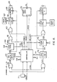
- FIG. 8 is a detailed block diagram of the system that measures mechanical and electrical skew to high resolution without using extremely high speed logic.
- FIG. 8 shows the elements for a two laser system, with channel 0, being nearly identical to channel 1. The only difference is that channel 0 contains an additional AND gate 60. Since the operation of both channels is nearly the same, only the operation of channel 0 will be discussed in detail.
- the high resolution programmable delay line 63 permits accurate indirect time measurement. Since the process is a nulling type scheme referencing the relative position of different beams, the absolute accuracy of the programmable delay line is not important. Second, electrical skew is included in the measurement by energizing the laser at a time at which its beam is nearly finished traversing the aligned sensor.
- FIG. 8 shows a controller 61 receiving the start of scan signal from element 50.
- Controller 61 loads a count into the down counter 64 for beginning the alignment process.
- Programmable delay line 63 provides the sub-pel correction and the total delay is passed through OR gate 65 and AND gate 60 to the laser control circuit 66.
- Control circuit 66 also receives image data 67 in order to modulate the laser driver 68, which energizes the laser chip 69.
- the alignment signal from the sensing element 51 is received by the beam on alignment sensor latch (BOAS latch) 70. Since the alignment sensor signal can be a very brief duration, the latch 70 is utilized.
- BOAS latch beam on alignment sensor latch
- FIG. 9A shows various timing events in the circuit of FIG. 8.
- FIG. 9B is an expansion of the timing around the sync position.
- Controller 61 is the timing center and decision making element for the system. It generates a signal "SOS PWR" for every scan. That signal is input to AND gate 60.
- the result is that the reference laser is turned on at a time in which it can energize the first element of the SOS sensor 50 and thereby generate the SOS signal.
- the SOS signal is the synchronization signal for the entire system.
- the SOS PWR signal remains active until controller 61 detects the rise of SOS.
- Controller 61 On each scan, the gated clock signal which is produced by precision oscillator 71, is resynchronized upon detector of SOS. Controller 61 then generates the reset and sync signals via a logical combination of the trailing edge of SOS and gated clock signals.
- Controller 61 determines the amount of delay set in the programmable delay line 63, via the multiple lines labeled CFO.
- the program delay line 63 is the fine delay mechanism typically having a 1 or 2 nanosecond step size. Controller 61 also determines the amount of full pel delay required by supplying the proper counter load value CCO for the down counter 64. Down counter 64 provides the course delay for the system. When controller 61 issues the reset command, CCO is loaded into down counters 64, along with the setting of the latch 70. At this time, the output latch 70 goes to a high level as shown in FIG. 9A.
- the sync signal is the start of timing events for the scan timing correction system and is generated by controller 61 a specific number of clock cycles after the activation of the SOS signal.
- the sync signal is one input to the AND gate 62, and must make its transitions when the clock signal is low.
- the sync signal remains low for several clock cycles to guarantee that the programmable delay line 63 clears out and remains low.
- Controller 61 must guarantee that the rising edge of the sync pulse is repeatable with respect to the falling edge of the start of scan signal on every scan.
- FIG. 10 is an illustration of a second embodiment of the invention.
- a charge coupled device (CCD) array 80 is used in place of the dual element start of scan sensor 35.
- Array 80 is located in the optical system shown in FIG. 2 at approximately the same location as the sensor element 35.
- CCD array 80 is designed to sense the position of the laser beams relative to each other.
- CCD arrays are a series of semiconductor elements similar to a photodiode, such that when light strikes the element a capacitor associated with the element is charged. The amount of charge is determined by the energy supplied, that is, the intensity of the light during the period of time over which the light strikes the semiconductor.
- CCD arrays can be either one dimensional or two dimensional, and in this case, a one dimensional CCD array 80 is used, as shown in FIG. 10.
- the array has electronics associated with it, such that the amount of energy supplied to any particular semiconductor can be ascertained.
- an N element array is utilized in the array shown in FIG. 10.
- the reference laser beam 40 is turned on at some point during the traversing of the CCD array.
- the reference beam 40 is sensed during the traversing of CCD element 3, as shown in FIG. 10, at trace A.
- Trace B illustrates that the energy associated with element 3 has risen a substantial amount, as shown at 40′, over the zero energy level at CCD element 2.
- the energy associated with the elements of the CCD array are all at a maximum level 40 ⁇ .
- the CCD array 80 has ascertained that the reference laser beam 40 turned on during the traversing of element 3.
- a programmable delay line such as previously described, is used in order to reposition the laser beam 40 turn on point, such that full energy at element 3 is accurately positioned.
- a programmable delay line provides a succession of pulses as shown at M-Q during the period in which the beam traverses element 3, and thereby the transition (turn-on point of laser beam 40) is sensed as occurring between taps P and Q of the programmable delay line.
- One advantage of the CCD array embodiment is that if a particular lasing beam is brighter or larger in spot size than another laser, the full energy point is still exactly the same regardless of which laser beam is striking the CCD array.
- the absolute value of the energy is not measured, but rather the position at shich the laser spot reaches full energy. Since the measurements are made for the turn on of the laser beams, electrical propagation delay as well as mechanical misalignment is factored into the positioning process.
Landscapes
- Engineering & Computer Science (AREA)
- Multimedia (AREA)
- Signal Processing (AREA)
- Physics & Mathematics (AREA)
- General Physics & Mathematics (AREA)
- General Engineering & Computer Science (AREA)
- Optics & Photonics (AREA)
- Theoretical Computer Science (AREA)
- Facsimile Scanning Arrangements (AREA)
- Dot-Matrix Printers And Others (AREA)
- Laser Beam Printer (AREA)
- Exposure Or Original Feeding In Electrophotography (AREA)
- Mechanical Optical Scanning Systems (AREA)
Applications Claiming Priority (2)
| Application Number | Priority Date | Filing Date | Title |
|---|---|---|---|
| US07/388,534 US4978849A (en) | 1989-08-01 | 1989-08-01 | Pel placement correction in the scan dimension of a multiple beam laser scanning system |
| US388534 | 1989-08-01 |
Publications (3)
| Publication Number | Publication Date |
|---|---|
| EP0412036A2 true EP0412036A2 (fr) | 1991-02-06 |
| EP0412036A3 EP0412036A3 (en) | 1992-07-08 |
| EP0412036B1 EP0412036B1 (fr) | 1995-09-06 |
Family
ID=23534512
Family Applications (1)
| Application Number | Title | Priority Date | Filing Date |
|---|---|---|---|
| EP90480085A Expired - Lifetime EP0412036B1 (fr) | 1989-08-01 | 1990-06-19 | Correction de positionnement d'éléments d'image dans la plage de balayage d'un système de balayage à laser à faisceaux multiples |
Country Status (5)
| Country | Link |
|---|---|
| US (1) | US4978849A (fr) |
| EP (1) | EP0412036B1 (fr) |
| JP (1) | JPH07102713B2 (fr) |
| CA (1) | CA2018497C (fr) |
| DE (1) | DE69022148T2 (fr) |
Cited By (10)
| Publication number | Priority date | Publication date | Assignee | Title |
|---|---|---|---|---|
| EP0534328A3 (en) * | 1991-09-26 | 1993-08-25 | Minolta Camera Kabushiki Kaisha | Recording apparatus having alterable recording density |
| EP0612185A1 (fr) * | 1993-02-19 | 1994-08-24 | Hollandse Signaalapparaten B.V. | Appareil de balayage optique |
| EP0620670A1 (fr) * | 1993-04-12 | 1994-10-19 | Presstek, Inc. | Procédé et appareil pour la correction et l'ajustement de la sortie d'images numériques |
| EP0620671A1 (fr) * | 1993-04-15 | 1994-10-19 | Konica Corporation | Appareil de formation d'image à rayons multiples |
| EP0709707A3 (fr) * | 1994-10-25 | 1997-07-09 | Fujitsu Ltd | Méthode d'exposition pour un appareil de formation d'image, et appareil de formation d'image |
| US5942745A (en) * | 1997-12-17 | 1999-08-24 | Presstek, Inc. | Method and apparatus for digital imaging with reduced periodic artifacts |
| EP0923222A3 (fr) * | 1997-12-10 | 2000-05-31 | Canon Kabushiki Kaisha | Dispositif de formation d'image |
| US6087069A (en) * | 1999-04-16 | 2000-07-11 | Presstek, Inc. | Lithographic imaging and cleaning of printing members having boron ceramic layers |
| US6222577B1 (en) | 1999-01-26 | 2001-04-24 | Presstek, Inc. | Multiple-beam, diode-pumped imaging system |
| EP2299390A3 (fr) * | 2009-09-14 | 2013-08-28 | Ricoh Company Ltd. | Dispositif d'écriture optique, appareil de formation d'images et procédé d'écriture optique |
Families Citing this family (17)
| Publication number | Priority date | Publication date | Assignee | Title |
|---|---|---|---|---|
| JPH03119308A (ja) * | 1989-10-02 | 1991-05-21 | Minolta Camera Co Ltd | レーザプリンタの書出し位置制御装置 |
| US5225848A (en) * | 1989-12-27 | 1993-07-06 | Am International, Inc. | Imaging diode array and system |
| US5081477A (en) * | 1990-03-26 | 1992-01-14 | International Business Machines Corporation | Method and apparatus for synchronizing the pel clock of a laser printer |
| EP0465074B1 (fr) * | 1990-06-27 | 1995-11-15 | Konica Corporation | Appareil pour former des images |
| US5172161A (en) * | 1990-12-31 | 1992-12-15 | Texas Instruments Incorporated | Unibody printing system and process |
| US5168167A (en) * | 1991-01-31 | 1992-12-01 | International Business Machines Corporation | Optical scanner having controllable light sources |
| US5374993A (en) * | 1991-10-01 | 1994-12-20 | Xerox Corporation | Image skew adjustment for a raster output scanning (ROS) system |
| US5394175A (en) * | 1992-12-18 | 1995-02-28 | Xerox Corporation | Transverse image registration for a digital color printer |
| JP2596639Y2 (ja) * | 1993-12-08 | 1999-06-21 | 株式会社キーエンス | レーザマーキング装置 |
| JP3291906B2 (ja) * | 1994-04-11 | 2002-06-17 | キヤノン株式会社 | 走査光学装置 |
| KR100292183B1 (ko) * | 1997-06-25 | 2001-09-28 | 이토가 미찌야 | 광빔특성평가방법 |
| US5966231A (en) * | 1998-08-07 | 1999-10-12 | Lexmark International, Inc. | Method and apparatus for aligning multiple laser beams |
| US6411322B1 (en) | 1999-07-15 | 2002-06-25 | International Business Machines Corporation | Test pattern for use to adjust multiple beam spot spacing |
| US7639407B2 (en) * | 2004-03-24 | 2009-12-29 | Lexmark International, Inc. | Systems for performing laser beam linearity correction and algorithms and methods for generating linearity correction tables from data stored in an optical scanner |
| US7570386B2 (en) * | 2005-09-15 | 2009-08-04 | Lexmark International, Inc. | Systems and methods that compensate for scan path errors in a multi-beam electrophotographic imaging apparatus |
| US9429285B2 (en) | 2012-12-11 | 2016-08-30 | Avago Technologies General Ip (Singapore) Pte. Ltd. | Downlight auxiliary ring |
| CN116382042B (zh) * | 2023-04-12 | 2025-09-19 | 深圳市先地图像科技有限公司 | 激光直写设备的数据处理方法、数据处理系统及相关设备 |
Family Cites Families (18)
| Publication number | Priority date | Publication date | Assignee | Title |
|---|---|---|---|---|
| JPS6033019B2 (ja) * | 1978-06-05 | 1985-07-31 | 株式会社日立製作所 | 光記録装置 |
| JPS569763A (en) * | 1979-07-06 | 1981-01-31 | Canon Inc | Beam recording device |
| US4393387A (en) * | 1979-09-14 | 1983-07-12 | Canon Kabushiki Kaisha | Beam recording apparatus effecting the recording by a plurality of beams |
| JPS5667277A (en) * | 1979-11-05 | 1981-06-06 | Canon Inc | Laser recording device |
| US4443695A (en) * | 1980-01-25 | 1984-04-17 | Canon Kabushiki Kaisha | Apparatus for controlling the quantity of light |
| JPS5764718A (en) * | 1980-10-09 | 1982-04-20 | Hitachi Ltd | Laser beam printer |
| JPS5767375A (en) * | 1980-10-14 | 1982-04-23 | Canon Inc | Multibeam recorder |
| US4404571A (en) * | 1980-10-14 | 1983-09-13 | Canon Kabushiki Kaisha | Multibeam recording apparatus |
| JPS57102609A (en) * | 1980-12-18 | 1982-06-25 | Canon Inc | Method and device for scanning using plural number of beams |
| JPS57116314A (en) * | 1981-01-12 | 1982-07-20 | Canon Inc | Image recorder on multilaser beam scanning system |
| JPS57204983A (en) * | 1981-06-10 | 1982-12-15 | Canon Inc | Scan type recording device |
| JPS5876857A (ja) * | 1981-11-02 | 1983-05-10 | Comput Basic Mach Technol Res Assoc | 記録装置 |
| JPS59162514A (ja) * | 1983-03-08 | 1984-09-13 | Dainippon Screen Mfg Co Ltd | 画像走査記録装置における焦点調整方法 |
| US4739415A (en) * | 1984-05-01 | 1988-04-19 | Canon Kabushiki Kaisha | Image handling system capable of varying the size of a recorded image |
| JPH0694215B2 (ja) * | 1985-04-24 | 1994-11-24 | 株式会社日立製作所 | レーザプリンタ装置及びその走査方法 |
| DE3750859T2 (de) * | 1986-06-07 | 1995-04-27 | Konishiroku Photo Ind | Bildaufzeichnungsvorrichtung. |
| JPS63163871A (ja) * | 1986-12-26 | 1988-07-07 | Toshiba Corp | 画像形成装置 |
| JPS63217763A (ja) * | 1987-03-06 | 1988-09-09 | Hitachi Ltd | 光プリンタ |
-
1989
- 1989-08-01 US US07/388,534 patent/US4978849A/en not_active Expired - Lifetime
-
1990
- 1990-06-07 CA CA002018497A patent/CA2018497C/fr not_active Expired - Fee Related
- 1990-06-19 EP EP90480085A patent/EP0412036B1/fr not_active Expired - Lifetime
- 1990-06-19 DE DE69022148T patent/DE69022148T2/de not_active Expired - Fee Related
- 1990-06-29 JP JP2174341A patent/JPH07102713B2/ja not_active Expired - Lifetime
Cited By (15)
| Publication number | Priority date | Publication date | Assignee | Title |
|---|---|---|---|---|
| EP0534328A3 (en) * | 1991-09-26 | 1993-08-25 | Minolta Camera Kabushiki Kaisha | Recording apparatus having alterable recording density |
| EP0612185A1 (fr) * | 1993-02-19 | 1994-08-24 | Hollandse Signaalapparaten B.V. | Appareil de balayage optique |
| US5629516A (en) * | 1993-02-19 | 1997-05-13 | Hollandse Signaalapparaten B.V. | Optical scanning apparatus with the rotation of array into two directions |
| US5453777A (en) * | 1993-04-12 | 1995-09-26 | Presstek, Inc. | Method and apparatus for correcting and adjusting digital image output |
| EP0620670A1 (fr) * | 1993-04-12 | 1994-10-19 | Presstek, Inc. | Procédé et appareil pour la correction et l'ajustement de la sortie d'images numériques |
| EP0620671A1 (fr) * | 1993-04-15 | 1994-10-19 | Konica Corporation | Appareil de formation d'image à rayons multiples |
| US5426528A (en) * | 1993-04-15 | 1995-06-20 | Konica Corporation | Correction device of light beam deviation of primary scanning direction thereof in image forming apparatus |
| EP0709707A3 (fr) * | 1994-10-25 | 1997-07-09 | Fujitsu Ltd | Méthode d'exposition pour un appareil de formation d'image, et appareil de formation d'image |
| US5724087A (en) * | 1994-10-25 | 1998-03-03 | Fujitsu Limited | Image forming apparatus and method for correcting a scanning line bend |
| EP0923222A3 (fr) * | 1997-12-10 | 2000-05-31 | Canon Kabushiki Kaisha | Dispositif de formation d'image |
| US6433909B2 (en) | 1997-12-10 | 2002-08-13 | Canon Kabushiki Kaisha | Image forming apparatus |
| US5942745A (en) * | 1997-12-17 | 1999-08-24 | Presstek, Inc. | Method and apparatus for digital imaging with reduced periodic artifacts |
| US6222577B1 (en) | 1999-01-26 | 2001-04-24 | Presstek, Inc. | Multiple-beam, diode-pumped imaging system |
| US6087069A (en) * | 1999-04-16 | 2000-07-11 | Presstek, Inc. | Lithographic imaging and cleaning of printing members having boron ceramic layers |
| EP2299390A3 (fr) * | 2009-09-14 | 2013-08-28 | Ricoh Company Ltd. | Dispositif d'écriture optique, appareil de formation d'images et procédé d'écriture optique |
Also Published As
| Publication number | Publication date |
|---|---|
| CA2018497A1 (fr) | 1991-02-01 |
| JPH03162973A (ja) | 1991-07-12 |
| DE69022148D1 (de) | 1995-10-12 |
| CA2018497C (fr) | 1995-06-27 |
| EP0412036A3 (en) | 1992-07-08 |
| US4978849A (en) | 1990-12-18 |
| JPH07102713B2 (ja) | 1995-11-08 |
| EP0412036B1 (fr) | 1995-09-06 |
| DE69022148T2 (de) | 1996-05-02 |
Similar Documents
| Publication | Publication Date | Title |
|---|---|---|
| EP0412036B1 (fr) | Correction de positionnement d'éléments d'image dans la plage de balayage d'un système de balayage à laser à faisceaux multiples | |
| JP2584111B2 (ja) | 画素位置を修正する方法 | |
| EP0797343B1 (fr) | Dispositif de commande de position de balayage d'un faisceau pour commander la position de balayage d'un faisceau, et dispositif de formation d'image utilisant ceci | |
| US6646668B2 (en) | Image forming apparatus for maintaining a constant beam scanning state | |
| US20050146596A1 (en) | Pixel clock and pulse-modulation-signal generating device, optical scanner, and image forming apparatus | |
| US5138479A (en) | Light beam scanning apparatus and method of detecting a variation of a scanning speed of a light beam | |
| EP0452242B1 (fr) | Méthode et appareil pour synchroniser l'horloge pour les éléments d'image dans une imprimante à laser | |
| EP0304276B1 (fr) | Appareil d'enregistrement à rayons | |
| US5347298A (en) | Exposure control device for use in electrophotographic printing apparatus | |
| US6219085B1 (en) | Method and system for improved performance of adjustable printer clocks in an electrophotographic device | |
| US5321432A (en) | Image forming apparatus with resolution control | |
| US6466247B1 (en) | Timing control of light beam scan | |
| JPH10232357A (ja) | 光走査装置 | |
| US6181357B1 (en) | Method and system for the modification of the timing of a plurality of PEL clocks in an electrophotographic device | |
| US20050030500A1 (en) | Apparatus for forming pattern | |
| US5341156A (en) | Image forming apparatus of laser scanning type | |
| JP3471060B2 (ja) | 画像形成装置の同期信号発生装置 | |
| JP3228316B2 (ja) | 光ビーム走査装置の書き込みタイミング制御装置 | |
| JP2965527B2 (ja) | 画像形成装置 | |
| JP4235292B2 (ja) | 画像形成装置 | |
| US20070285492A1 (en) | Laser Power Switching for Alignment Purposes in a Laser Printer | |
| JP2001051216A (ja) | 光ビーム走査制御回路及びそれを用いた光学ユニット並びに画像形成装置 | |
| US20060262331A1 (en) | Image forming apparatus and image forming method | |
| JPH04305670A (ja) | 印字装置 | |
| JPS62267774A (ja) | レ−ザカラ−プリンタ |
Legal Events
| Date | Code | Title | Description |
|---|---|---|---|
| PUAI | Public reference made under article 153(3) epc to a published international application that has entered the european phase |
Free format text: ORIGINAL CODE: 0009012 |
|
| 17P | Request for examination filed |
Effective date: 19901213 |
|
| AK | Designated contracting states |
Kind code of ref document: A2 Designated state(s): DE FR GB IT |
|
| PUAL | Search report despatched |
Free format text: ORIGINAL CODE: 0009013 |
|
| AK | Designated contracting states |
Kind code of ref document: A3 Designated state(s): DE FR GB IT |
|
| 17Q | First examination report despatched |
Effective date: 19940324 |
|
| GRAA | (expected) grant |
Free format text: ORIGINAL CODE: 0009210 |
|
| AK | Designated contracting states |
Kind code of ref document: B1 Designated state(s): DE FR GB IT |
|
| PG25 | Lapsed in a contracting state [announced via postgrant information from national office to epo] |
Ref country code: IT Free format text: LAPSE BECAUSE OF FAILURE TO SUBMIT A TRANSLATION OF THE DESCRIPTION OR TO PAY THE FEE WITHIN THE PRESCRIBED TIME-LIMIT;WARNING: LAPSES OF ITALIAN PATENTS WITH EFFECTIVE DATE BEFORE 2007 MAY HAVE OCCURRED AT ANY TIME BEFORE 2007. THE CORRECT EFFECTIVE DATE MAY BE DIFFERENT FROM THE ONE RECORDED. Effective date: 19950906 Ref country code: FR Effective date: 19950906 |
|
| REF | Corresponds to: |
Ref document number: 69022148 Country of ref document: DE Date of ref document: 19951012 |
|
| EN | Fr: translation not filed | ||
| PLBE | No opposition filed within time limit |
Free format text: ORIGINAL CODE: 0009261 |
|
| STAA | Information on the status of an ep patent application or granted ep patent |
Free format text: STATUS: NO OPPOSITION FILED WITHIN TIME LIMIT |
|
| 26N | No opposition filed | ||
| PGFP | Annual fee paid to national office [announced via postgrant information from national office to epo] |
Ref country code: GB Payment date: 19990527 Year of fee payment: 10 |
|
| PG25 | Lapsed in a contracting state [announced via postgrant information from national office to epo] |
Ref country code: GB Free format text: LAPSE BECAUSE OF NON-PAYMENT OF DUE FEES Effective date: 20000619 |
|
| GBPC | Gb: european patent ceased through non-payment of renewal fee |
Effective date: 20000619 |
|
| PGFP | Annual fee paid to national office [announced via postgrant information from national office to epo] |
Ref country code: DE Payment date: 20020715 Year of fee payment: 13 |
|
| PG25 | Lapsed in a contracting state [announced via postgrant information from national office to epo] |
Ref country code: DE Free format text: LAPSE BECAUSE OF NON-PAYMENT OF DUE FEES Effective date: 20040101 |