EP0412426A2 - Emetteur auto-oscillant en mode burst avec un nombre entier de périodes - Google Patents
Emetteur auto-oscillant en mode burst avec un nombre entier de périodes Download PDFInfo
- Publication number
- EP0412426A2 EP0412426A2 EP90114784A EP90114784A EP0412426A2 EP 0412426 A2 EP0412426 A2 EP 0412426A2 EP 90114784 A EP90114784 A EP 90114784A EP 90114784 A EP90114784 A EP 90114784A EP 0412426 A2 EP0412426 A2 EP 0412426A2
- Authority
- EP
- European Patent Office
- Prior art keywords
- oscillatory
- tank circuit
- signal
- peak
- waveform
- Prior art date
- Legal status (The legal status is an assumption and is not a legal conclusion. Google has not performed a legal analysis and makes no representation as to the accuracy of the status listed.)
- Granted
Links
Images

Classifications
-
- H—ELECTRICITY
- H03—ELECTRONIC CIRCUITRY
- H03B—GENERATION OF OSCILLATIONS, DIRECTLY OR BY FREQUENCY-CHANGING, BY CIRCUITS EMPLOYING ACTIVE ELEMENTS WHICH OPERATE IN A NON-SWITCHING MANNER; GENERATION OF NOISE BY SUCH CIRCUITS
- H03B5/00—Generation of oscillations using amplifier with regenerative feedback from output to input
- H03B5/08—Generation of oscillations using amplifier with regenerative feedback from output to input with frequency-determining element comprising lumped inductance and capacitance
- H03B5/12—Generation of oscillations using amplifier with regenerative feedback from output to input with frequency-determining element comprising lumped inductance and capacitance active element in amplifier being semiconductor device
- H03B5/1206—Generation of oscillations using amplifier with regenerative feedback from output to input with frequency-determining element comprising lumped inductance and capacitance active element in amplifier being semiconductor device using multiple transistors for amplification
- H03B5/1221—Generation of oscillations using amplifier with regenerative feedback from output to input with frequency-determining element comprising lumped inductance and capacitance active element in amplifier being semiconductor device using multiple transistors for amplification the amplifier comprising multiple amplification stages connected in cascade
-
- H—ELECTRICITY
- H03—ELECTRONIC CIRCUITRY
- H03B—GENERATION OF OSCILLATIONS, DIRECTLY OR BY FREQUENCY-CHANGING, BY CIRCUITS EMPLOYING ACTIVE ELEMENTS WHICH OPERATE IN A NON-SWITCHING MANNER; GENERATION OF NOISE BY SUCH CIRCUITS
- H03B5/00—Generation of oscillations using amplifier with regenerative feedback from output to input
- H03B5/08—Generation of oscillations using amplifier with regenerative feedback from output to input with frequency-determining element comprising lumped inductance and capacitance
- H03B5/12—Generation of oscillations using amplifier with regenerative feedback from output to input with frequency-determining element comprising lumped inductance and capacitance active element in amplifier being semiconductor device
- H03B5/1228—Generation of oscillations using amplifier with regenerative feedback from output to input with frequency-determining element comprising lumped inductance and capacitance active element in amplifier being semiconductor device the amplifier comprising one or more field effect transistors
-
- H—ELECTRICITY
- H03—ELECTRONIC CIRCUITRY
- H03B—GENERATION OF OSCILLATIONS, DIRECTLY OR BY FREQUENCY-CHANGING, BY CIRCUITS EMPLOYING ACTIVE ELEMENTS WHICH OPERATE IN A NON-SWITCHING MANNER; GENERATION OF NOISE BY SUCH CIRCUITS
- H03B11/00—Generation of oscillations using a shock-excited tuned circuit
- H03B11/04—Generation of oscillations using a shock-excited tuned circuit excited by interrupter
- H03B11/10—Generation of oscillations using a shock-excited tuned circuit excited by interrupter interrupter being semiconductor device
-
- H—ELECTRICITY
- H04—ELECTRIC COMMUNICATION TECHNIQUE
- H04B—TRANSMISSION
- H04B1/00—Details of transmission systems, not covered by a single one of groups H04B3/00 - H04B13/00; Details of transmission systems not characterised by the medium used for transmission
- H04B1/02—Transmitters
- H04B1/04—Circuits
- H04B2001/0491—Circuits with frequency synthesizers, frequency converters or modulators
Definitions
- the present invention relates to an efficient self-oscillating burst mode transmitter or oscillator used with implantable devices, such as medical devices. More particularly, the present invention relates to a self-oscillating burst mode transmitter or oscillator wherein each burst of the transmitted or generated output signal contains an integral number of periods of a carrier signal at a substantially constant amplitude.
- the invention finds primary application in communicating with an implantable medical device, such as a pacemaker.
- Burst mode transmitters or oscillators transmit or generate a carrier signal for a short period of time, termed the "burst" time, and do not transmit or generate the carrier signal in between burst times, or “bursts.”
- Such transmitters or oscillators are commonly used in communication channels, e.g., where digital data is transferred using an ON-OFF keyed encoding scheme.
- the presence of a carrier signal indicates one binary value, such as a binary "1”
- the absence of the carrier signal indicates the other binary value, such as a binary "0".
- a burst mode transmitter may be used to transmit one binary value through the transmission of a burst, and to transmit the other binary value through the absence of a burst.
- burst mode transmitters or oscillators may be classified as: (1) self-oscillating, in which case the carrier signal is generated by the transmitter or oscillator upon application of power thereto; or (2) clock-driven, in which case an external clock signal provides the basic signal from which the carrier signal is derived.
- the self-oscillating type of transmitter or oscillator may operate in two modes.
- a first mode is a continuous mode, in which case the carrier signal is generated continuously (100% duty cycle), with a burst of the carrier signal being obtained by gating the carrier signal for the desired burst time, and blocking it in between burst times. This gated signal is then applied to a transmitting coil (or other load).
- a second mode is a burst mode, in which case the carrier signal is generated only during the desired burst time period (less than 100% duty cycle), and is not generated during non-burst time periods.
- Clock-driven oscillators as defined above, always operate in the continuous mode because the basic clock signal is always present at a 100% duty cycle.
- Continuous mode operation of a burst mode transmitter or oscillator is inefficient. That is, a significant amount of power may be consumed during the non-burst periods when operation of the transmitter or oscillator is not needed.
- the ideal burst mode transmitter or oscillator from a power efficient stand point, is ON only when transmitting or generating a burst of the carrier signal, and OFF at all other times.
- a self-oscillating burst mode transmitter is generally not able to operate at maximum efficiency. This is because the carrier signal must typically be applied to an inductive load (transmitting coil or antenna), and the transient response associated with suddenly applying a signal to an inductive load prevents the applied carrier signal from assuming its maximum value (amplitude) across the inductive load throughout the entire duration of the transmitted burst. Hence, a portion of each burst, typically more than one cycle of the carrier signal, must usually be transmitted at less than maximum power. While this effect can be minimized by increasing the duration of the burst, such increase of burst time may significantly slow down the rate at which data can be transferred (the burst rate).
- the tank circuit consists of an inductor and a capacitor connected in a suitable series or parallel circuit configuration.
- the tank circuit When the tank circuit is energized with power of an appropriate polarity, the tank circuit begins to resonate at its resonant frequency.
- the resonant frequency of a tank circuit is a function of the inductor and capacitor values used therein.
- the oscillations at the resonant frequency continue. Unfortunately, it typically takes several cycles of the resonating carrier signal before a steady-state oscillatory condition exists within the tank circuit.
- the number of cycles appearing in a given burst has been only approximately determined by controlling the duration of the transmitted burst from an external time base. What is needed is a more precise technique for controlling the number of cycles of the carrier signal appearing in each burst, and more particularly a technique that accurately places a programmable integral number of cycles of the carrier signal in each burst.
- the present invention advantageously addresses the above and other needs.
- the present invention is directed to a self-oscillating burst mode transmitter that transmits an integral number of carrier signal cycles in each transmission burst.
- each transmitted burst commences at a peak voltage value of the carrier signal and terminates at a peak voltage value, with this peak voltage value being stored in the tank circuit in between bursts.
- Storing of the peak voltage value advantageously avoids transient problems associated with switched inductive loads, thereby allowing the burst to always be transmitted efficiently at full power.
- the transmitter includes an L-C tank circuit comprising a transmitting coil connected to a capacitor.
- the L-C tank circuit is selectively energized through a switching network connected to a power source. When switchably energized, the tank circuit resonates at a prescribed frequency. Selective energization of the tank circuit through the switching network is controlled by a peak voltage detection circuit.
- the peak detection circuit senses when a peak voltage is present in the oscillatory waveform appearing across the coil of the resonating tank circuit, and when the polarity of the power connected to the tank circuit should be reversed.
- the switching network removes (switches off) power from the tank circuit, i.e., does not allow power of either polarity to be connected to the tank circuit.
- this switching off of the power occurs only when the oscillatory voltage waveform, as sensed by the peak detection circuit, is at a maximum value, or peak. (This maximum value may be either positive or negative.)
- the peak voltage is stored by the capacitor of the tank circuit, which capacitor maintains (stores) this peak voltage during the time the power source is not connected to the tank circuit.
- the voltage initially appearing across the coil, and hence the voltage at the commencement of the next oscillatory waveform of the transmission burst begins at the peak voltage value stored on the capacitor.
- the transmitted burst begins at a peak voltage and ends at a peak voltage, with an integral number of cycles occurring in the burst.
- the peak detection circuit is realized using a phase shift network and a zero crossing detector.
- the phase shift network shifts the phase of the voltage waveform developed across the coil of the tank circuit by 90 degrees.
- the zero crossings of this phase shifted signal which are easily detected in a comparator circuit, then mark the peaks of the coil voltage.
- the occurrence of such peaks in the coil voltage are then used in appropriate logic circuits for controlling the switching network that connects and disconnects the power source to the tank circuit. For example, only at the occurrence of a peak coil voltage as above described is the polarity of the power connected to the tank circuit via the switching network reversed, thereby assuring maximum energy transfer to the tank circuit.
- the present invention may thus be characterized, in accordance with one variation thereof, as a self-oscillating burst mode transmitter that comprises: (1) an L-C tank circuit that includes a transmitting coil connected to a capacitor; (2) switch means responsive to a control signal for switchably connecting an energy source to the L-C tank circuit, causing the L-C tank circuit to oscillate at a resonant frequency, an oscillatory voltage waveform being developed across the transmitting coil and capacitor as the tank circuit oscillates; (3) phase shift means coupled to the transmitting coil for generating an output voltage signal having the same frequency as the oscillatory voltage waveform, this output voltage signal having a phase angle that is shifted from the phase angle of the oscillatory voltage waveform by a prescribed amount; (4) comparator means for comparing the amplitude of the output voltage signal generated by the phase shift means with a reference signal, and for generating the control signal as a function of whether the amplitude of the output voltage signal is less than or greater than the reference signal; and (5) inhibiting means for selectively
- the tank circuit starts its next oscillatory cycle (when not inhibited by the inhibiting means) with the voltage waveform across the transmitter coil being at the stored peak voltage value; and stops its oscillatory cycle with the voltage waveform across the transmitter coil being at a corresponding peak voltage value. In this way, an integral number of periods of the oscillating voltage waveform occur between the time the oscillatory cycle starts and stops.
- the present invention may be characterized as a burst mode integer period oscillator that includes: (1) a tank circuit including a coil connected to a capacitor; (2) switch means for delivering power to the tank circuit, the tank circuit oscillating at a resonant frequency in response to the delivered power, thereby causing an oscillatory voltage waveform to be developed across the coil and capacitor as the tank circuit oscillates; (3) sensing means for sensing when the oscillatory voltage waveform is at a peak value; and (4) inhibiting means synchronized with the sensing means for selectively stopping the delivery of the power to the tank circuit at a time when the oscillatory voltage waveform developed across the coil and capacitor is at a peak voltage value.
- the capacitor of the tank circuit stores the peak voltage value until the inhibiting means allows power to be delivered to the tank circuit, at which time the tank circuit again begins to oscillate at the resonant frequency, with the oscillatory voltage waveform beginning at the peak voltage value stored by the capacitor.
- the tank circuit starts an oscillatory cycle (when allowed by the inhibiting means) at a time when the voltage waveform across the transmitter coil is at a first peak value.
- the tank circuit stops the oscillatory cycle (as controlled by the inhibiting means) at a time when the voltage waveform across the transmitter coil is at a second peak value.
- An integral number of periods of the oscillating voltage waveform occur between the first and second peak values, and are thus included within the signal burst of the oscillator.
- the invention includes a method of controlling a burst mode oscillator so that each burst contains an integral number of cycles.
- the oscillator used with this method includes a tank circuit that generates an oscillatory waveform having a prescribed frequency upon being energized with power from an external power source.
- the method includes the steps of: (a) energizing the tank circuit with power whenever a first burst of oscillations is desired; (b) sensing when the oscillatory waveform associated with the energized tank circuit is at a prescribed value; (c) selectively inhibiting the delivery of power to the tank circuit at the conclusion of the first burst of oscillations at a point within a cycle of the oscillatory waveform when the waveform sensed in step (b) is at a prescribed value; (d) storing the energy associated with the prescribed value of the oscillatory waveform during the time when the tank circuit is inhibited; and (e) starting the oscillatory waveform of the tank circuit, when next energized at the beginning of a second burst of oscillations, at the prescribed value stored within the tank circuit in step (d).
- a still further aspect of the invention provides an efficient burst mode transmitter or oscillator that periodically transmits or generates bursts of a carrier signal by selectively energizing a tank circuit, the resonant frequency of the tank circuit comprising the frequency of the carrier signal present in each burst.
- the tank circuit is not energized in between bursts, thereby conserving power. Nonetheless, once the tank circuit is energized, the carrier signal is immediately available at full power throughout the duration of the burst without significant transient effects and/or needless power consumption.
- Still another aspect of the invention provides such a burst mode transmitter or oscillator wherein an integral number of cycles of the carrier signal in each burst may be programmably selected.
- Another aspect of the invention provides a method of generating or transmitting an integral number of cycles of a carrier signal within each burst of a burst mode oscillator or transmitter.
- the peaks (or other prescribed points) of the carrier signal are detected, and are used to precisely control when a tank circuit, resonant at the carrier signal frequency, is connected or disconnected to a suitable power source.
- the tank circuit When connected to the power source, the tank circuit resonates for an integral number of cycles, thereby providing an integral number of carrier signal cycles.
- the tank circuit does not resonate, and no carrier signal is provided.
- Yet a further aspect of the invention is to provide an efficient self-oscillating burst mode transmitter and/or method of transmitting as above described wherein the transmitter and/or method are especially adapted for transmitting burst signals containing an integral number of carrier frequency cycles to or from an implanted device, such as an implanted medical device, e.g., a pacemaker.
- an implanted device such as an implanted medical device, e.g., a pacemaker.
- An external device 12 includes a transmitter that transmits a signal from a transmitting coil 14 to an implantable device 16, such as an implantable pacemaker.
- the device 16 is implanted beneath a layer of skin 20 of the person or animal in which the device is used.
- a receiving coil 18 is coupled to a receiver circuit included within the device 16. Both the receiver circuit 16 and the receiving coil 18 are placed within an sealed enclosure 22, typically made from stainless steel or some other body compatible substance.
- the transmitting coil 14 is positioned as close as possible to the receiving coil 18, e.g., within a few inches, and the two coils are inductively coupled to each other.
- a voltage signal V T appearing across the transmitting coil 14 is induced in the receiving coil 18, where it appears as a voltage signal V R .
- the two coils thus function much the same as an air coil transformer, with the voltage applied to the transmitting coil 14 being transferred to the receiving coil 18 as a function of the coupling coefficient between the two coils, which coupling coefficient is highly dependent upon the separation distance between the two coils and the medium separating the two coils (in this case, body flesh and air).
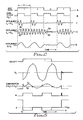
- FIG. 2 illustrates representative waveforms that may be used with the operation of a burst mode transmitter, such as the device 12 of FIG. 1. These waveforms are presented to define the various parameters that are typically used in specifying the operation of a burst mode transmitter or oscillator, and to further illustrate some examples of these parameters.
- Line A of FIG. 2 depicts digital NRZ (non return to zero) data having a bit period of T seconds. In accordance with the NRZ pattern shown, a digital "1" is represented as a high level, and a digital "0" is represented as a low level. Thus, the waveform shown on line A represents the digital data "1101".
- Line C shows a representative voltage waveform to be transmitted (e.g., to be applied to the transmitting coil 14 of FIG. 1) assuming a burst duration of 40% of the bit period, and further assuming a carrier frequency of 5f0.
- line D shows a representative voltage waveform to be transmitted assuming a burst duration of 100% of the bit period, and also assuming a carrier frequency of 5f0.
- the carrier frequency be the same as the bit rate, as shown in line E.
- the carrier frequency be the same as the bit rate, as shown in line E.
- this is not always possible.
- the waveform of line D in FIG. 2 further illustrates the manner in which the voltage to be transmitted in a given burst exponentially increases up to its maximum value, or exponentially decreases from its maximum value, in accordance with a fixed time constant (the effects of this time constant being represented in FIG. 2, line D, by the dashed line envelope 30). That is, every time there is a change in the data to be transmitted, the voltage waveform appearing across the load of the transmitter --a tank circuit-- does not change immediately. Rather, it changes gradually, following the time constant envelope, in accordance with well known transient circuit analysis principles. Unfortunately, the existence of this transient envelope in the signals to be transmitted exists in many prior art burst mode transmitters, and encumbers their efficient operation. This is because, as seen in FIG.
- the transmitted signal is not transmitted at full power throughout the entire duration of the bit period when the carrier signal is to be transmitted; and the absence of a transmitted signal is not possible throughout the entire duration of the bit period when the carrier signal is not be transmitted.
- the desired information to be transmitted is not transmitted efficiently.
- line D in FIG. 2 illustrates this exponentially increasing/decreasing transient condition
- line E may also exist in connection with the waveforms of lines C and E. If present in line E, for example, to the same extent as shown in line D (i.e., if the time constant were approximately the same value), and if less than a 100% burst duration were used, it is evident that there would not be much of a signal left to be transmitted during the burst. For this and other reasons, it is quite common for burst mode transmitters and oscillators to transmit several cycles of the carrier frequency in each transmitted burst, even though such transmission may require a significantly wider bandwidth.
- FIG. 3 a schematic/block diagram of the preferred embodiment of a self-oscillating burst mode transmitter made in accordance with the present invention is shown.
- a tank circuit comprising an inductor L1 and a capacitor C4.
- the capacitor C4 is switchably connected in parallel with the inductor L1, which inductor L1 functions as the transmitting coil, by way of FET transistor switch Q1 or FET transistor switch Q2.
- One side of the inductor L1 is connected to ground, and the other side is connected to one side of capacitor C4.
- the voltage of the tank circuit at the junction of the inductor L1 with the capacitor C4, measured relative to ground, is hereafter referred to as the core voltage, V L .
- Switch Q1 connects the side of capacitor C4 not connected to the inductor L1, labeled "A" in FIG. 3, to a positive voltage potential, +V DD , through a diode D2.
- the cathode of diode D2 is connected to the "A" side of capacitor C4, and the anode of D2 is connected to one leg of the switch Q1.
- the other leg of switch Q1 is connected to the power supply +V DD .
- Switch Q2 connects the "A" side of capacitor C4 to ground.
- switches Q1 and Q2 are controlled by logic signals obtained from the outputs of the NAND gate U1 and NOR gate U2, respectively.
- One input to each of these gates U1 and U2 is obtained from flip flop U3, with the Q output of U3 being connected to NAND gate U3, and the Q* output of U3 (where Q* is the inverse of Q) being connected to NOR gate U2.
- the flip flop U3 thus enables one of the gates U1 or U2 and disables the other one. This means that only one of the switches Q1 or Q2 may be ON at any given time. Further, as will also be explained below in connection with the description of FIG. 5, while only one of the switches Q1 or Q2 may be ON at any given time, both switches may be OFF at the same time.
- a first delay circuit is made up of a resistor R3 in parallel with a diode D3.
- a second delay circuit is made up of a resistor R4 in parallel with a diode D4.
- the first delay circuit is connected between the output of the invertor gate U4 and the input of NOR gate U2, with the cathode of diode D3 being connected to the NOR gate U2.
- the second delay circuit is connected between the output of the invertor gate U4 and the input of NAND gate U1, with the cathode of diode D4 being connected to the output of invertor U4.
- these delay circuits prevent switches Q1 and Q2 from being ON at the same time as one switches from ON to OFF, and the other switches from OFF to ON.
- the input to the invertor gate U4, and the signal that controls the operation of the transmitter when it is enabled, is the output signal from a comparator circuit 32.
- the comparator circuit 32 compares two input signals, one designated V0 connected to the non-inverting ("+") terminal, and the other designated V R connected to the inverting ("-") terminal, and produces an output signal, designated "B", that assumes one of two values. When the signal V0 is greater than the signal V R , the output signal "B" from the comparator 32 goes high. When the signal V0 is less than the signal V R , the output signal "B" from the comparator circuit 32 goes low.
- the "-" input terminal of the comparator circuit 32 is connected to ground (zero volts) through a resistor R1.
- the signal V R is normally a reference signal which assumes a value of zero volts.
- the "+" input terminal of the comparator circuit 32 is connected to the output of a phase shift network 34.
- the input to the phase shift network 34 is the load voltage V L appearing across the inductive transmitting coil L1 of the tank circuit.
- the preferred phase shift network 34 is a differentiator that shifts the phase of the load voltage V L by -90 degrees ( ⁇ /2 radians).
- the output voltage of the phase shift network 34 also assumes a substantially sinusoidal waveform that is shifted in phase relative to the load voltage V L by 90 degrees, or approximately 1/4 of a cycle.
- the zero crossings of the load voltage V L correspond in time to the peaks of the phase shift circuit output voltage V0
- the peaks of the load voltage V L correspond in time to the zero crossings of the voltage V0.
- the phase shift network 34 and the comparator circuit 32 accordingly function as a peak detection circuit for the load voltage V L .
- a first is a capacitor C3.
- This capacitor C3 functions as a “speed-up” capacitor that speeds up the comparator and invertor transitions.
- the speed-up capacitor C3 is connected between the "-" terminal of the comparator circuit 32 and the output of invertor gate U4. As thus connected, it provides, in effect, a positive feedback connection to the comparator circuit that assures a quick, non-oscillatory transition of the comparator output signal "B" from one state to another.
- the other circuit elements connected to the "-" terminal of the comparator 32 are a diode D1 and capacitor C1.
- the cathode of diode D1 is connected to the "-" terminal of the comparator 32.
- the anode of diode D1 is connected to the Q* output of flip flop U3.
- the capacitor C1 is connected in parallel with diode D1.
- the clock input of the flip flop U3 is connected to the "B" output of the comparator 32.
- Flip flop U3 is preferably a D-type flip flop, such as is obtained from 1/2 of a dual D flip flop CMOS 4013 device.
- the data D on its data input line is clocked to the Q output of the flip flop on the positive going transition of the clock signal.
- the Q output of flip flop U3 is set to the state of the input data D (and the Q* output of flip flop U3 is set to the inverse of the data D).
- the data D is connected to an ON/OFF control signal that enables or disables the transmitter.
- the ON/OFF control signal goes high, starting the burst.
- the ON/OFF signal goes low, and the burst stops at the occurrence of the next peak of a prescribed polarity of the load voltage V L after the ON/OFF control signal goes low.
- a capacitor C2 and a resistor R2 couple the ON/OFF control signal to the set terminal of the flip flop U3.
- the ON/OFF signal switches from a low level (turn off burst) to a high level (turn on burst)
- the reset terminal of flip flop U3 is also tied to ground. With both the set and reset terminals at a low level (ground), the flip flop functions as a normal D flip flop with its output signals being controlled by the value of the data D at the time of a positive clock transition.
- FIG. 4 shows a preferred circuit schematic diagram for the phase shift network 34.
- this circuit comprises a differentiator circuit that comprises two capacitors C5 and C6 connected in series. At the common junction point between these two capacitors C5 and C6, a resistor R5 is shunted to ground. Clamping diodes D5 and D6 are connected in parallel across resistor R5, with the anode of one being connected to the cathode of the other. These diodes limit the magnitude of the signal that may pass through the network 34, and thereby protect the input circuits of the comparator 32 from excessive input signal levels.
- Another resistor R6 is shunted to ground from the other side of capacitor C6, i.e., the side not connected to the common junction point between C5 and C6.
- the load voltage, V L is applied to one side of capacitor C5.
- the phase shifted or differentiated output voltage, V L appears at the junction of capacitor C6 and resistor R6.
- the waveform timing diagram of FIG. 5 shows the steady state operation of the circuit, after the circuit has been operating for one or more bursts.
- the transient start-up operation of the circuit is essentially the same as the steady state operation, once certain initial conditions are set. Initially, the noise on core L will be enough to trip the comparator 32 to one state, next to the opposite state, thus starting the oscillatory process.
- the low input at NAND gate U1 provides a "1" at the output, meaning that transistor switch Q1, which is a P-channel device, remains off. However, the low input at NOR gate U2 forces the output of the NOR gate to go high, and turns on transistor switch Q2, which is an N-channel device.
- the voltage at point "A" in the circuit goes to a voltage equal to the peak AC voltage of the tank circuit, and remains at that value for a time determined by the leakage current of the diode D2 and the switch Q2.
- this time can be relatively long, e.g., several seconds.
- the operation of the circuit as described above allows the burst voltage to always start and stop exactly at the peak voltage.
- This peak voltage may be considered as a maximum voltage, whether it is a negative peak voltage or a positive peak voltage. (A negative peak voltage is illustrated in FIG. 5.)
- the energy of the tank circuit is saved or stored on capacitor C4, so that the next burst starts with the same prior peak (maximum) voltage amplitude.
- the present invention requires a circuit to automatically control the number of cycles of the carrier signal which appear in each burst.
- a circuit such as the one shown in FIG. 6 may be used to accomplish the same function.
- the voltage appearing at point "A" in the circuit of FIG. 3 is applied to the input of an inverting buffer amplifier 38, or equivalent.
- a coupling capacitor C7 and clamping diode D7 are used to limit the voltage swing at the input of the amplifier 38.
- the output of the amplifier 38 is then applied to the clock input of a count down register 40.
- This count down register includes a strobe or load terminal, "L", that loads data thereinto when the strobe signal goes low.
- the register further includes an output signal Q0 that is high for so long as the register contents are non zero, and that goes low when the register contents are zero.
- a preselected number "n” is programmably stored in a memory device 42 and loaded into the register 40. The value of "n" is one less than the integral number of carrier cycles desired in the transmitter burst.
- the Q0 output signal from the register is high. As soon as the register is zero, the Q0 output signal goes low.
- This output signal is applied to an AND gate 44 where it is logically ANDED with a START signal.
- the output signal from the AND gate 44 may function as the ON/OFF command signal described above. So long as the START signal is high, and the Q0 signal is high, the ON/OFF command signal is also high. As soon as either the START signal or the Q0 signal goes low, however, the ON/OFF signal goes low, causing the transmitter to stop the burst at the conclusion of the next cycle of the load voltage V L .
- the value "n” is again loaded into the count down register 40 and the process repeats. In this manner, the register is reloaded with the value "n” at the desired burst rate, causing each burst to have n+1 cycles of the carrier signal therein.
- circuit components shown in FIGS. 3, 4 and 6 may be commercially available components available from numerous vendors at modest cost.
- the logic circuits for example, are preferably from the CMOS 4000 series. available from, e.g., RCA.
- the diodes may be 1N914 diodes, available from, e.g., Motorola.
- the transistor switches may be 1RFU9022 (Q1) and 1RFU110 (Q2).
- the comparator may be an LM393A. Equivalent components may, of course, also be used.
- the burst rate is approximately 8000 Hz, and one cycle of the carrier signal is included in each burst.
- the present invention provides a self-oscillating burst mode transmitter or oscillator that periodically transmits or generates bursts of a carrier signal at a prescribed rate wherein each burst includes an integral number of periods of the carrier signal. Further, the carrier signal starts and stops each burst at a peak value, and this peak value is advantageously stored and used as the starting voltage of the carrier signal at the commencement of the next burst.
- the transmitter thus provided is low in cost, efficient to operate, and reliable in performance. Further, in one embodiment, the number of integral cycles of the carrier signal included in each burst may be programmably selected.
- the invention also includes a method of generating or transmitting an integral number of cycles of a carrier signal within each burst of a burst mode oscillator or transmitter.
- the peaks of the carrier signal are detected, and are used to precisely control when a tank circuit, resonant at the carrier signal frequency, is connected or disconnected to the power source.
- the tank circuit When connected to the power source, the tank circuit resonates for an integral number of cycles, thereby providing an integral number of carrier signal cycles.
- the tank circuit does not resonate, and no carrier signal is provided.
Landscapes
- Transmitters (AREA)
- Synchronisation In Digital Transmission Systems (AREA)
- Electrotherapy Devices (AREA)
- Inductance-Capacitance Distribution Constants And Capacitance-Resistance Oscillators (AREA)
- Digital Transmission Methods That Use Modulated Carrier Waves (AREA)
Applications Claiming Priority (2)
| Application Number | Priority Date | Filing Date | Title |
|---|---|---|---|
| US391077 | 1989-08-08 | ||
| US07/391,077 US4980898A (en) | 1989-08-08 | 1989-08-08 | Self-oscillating burst mode transmitter with integral number of periods |
Publications (3)
| Publication Number | Publication Date |
|---|---|
| EP0412426A2 true EP0412426A2 (fr) | 1991-02-13 |
| EP0412426A3 EP0412426A3 (en) | 1991-09-18 |
| EP0412426B1 EP0412426B1 (fr) | 1993-08-04 |
Family
ID=23545132
Family Applications (1)
| Application Number | Title | Priority Date | Filing Date |
|---|---|---|---|
| EP90114784A Expired - Lifetime EP0412426B1 (fr) | 1989-08-08 | 1990-08-01 | Emetteur auto-oscillant en mode burst avec un nombre entier de périodes |
Country Status (5)
| Country | Link |
|---|---|
| US (1) | US4980898A (fr) |
| EP (1) | EP0412426B1 (fr) |
| JP (1) | JPH0622336B2 (fr) |
| AU (1) | AU616150B2 (fr) |
| DE (1) | DE69002560T2 (fr) |
Cited By (2)
| Publication number | Priority date | Publication date | Assignee | Title |
|---|---|---|---|---|
| EP0523271A1 (fr) * | 1991-07-18 | 1993-01-20 | Texas Instruments Deutschland Gmbh | Arrangement d'un circuit pour couplage d'antenne |
| EP0680148A3 (fr) * | 1994-04-18 | 1997-10-01 | At & T Corp | Circuit d'horloge à faible consommation. |
Families Citing this family (62)
| Publication number | Priority date | Publication date | Assignee | Title |
|---|---|---|---|---|
| US5717685A (en) * | 1989-04-28 | 1998-02-10 | Abraham; Charles | Transformer coupler for communication over various lines |
| US5383912A (en) * | 1993-05-05 | 1995-01-24 | Intermedics, Inc. | Apparatus for high speed data communication between an external medical device and an implantable medical device |
| US5475307A (en) * | 1994-07-29 | 1995-12-12 | Pacesetter, Inc. | Frequency demodulator and method for asynchronously demodulating sample signals |
| US6015406A (en) | 1996-01-09 | 2000-01-18 | Gyrus Medical Limited | Electrosurgical instrument |
| ES2154824T5 (es) | 1995-06-23 | 2005-04-01 | Gyrus Medical Limited | Instrumento electroquirurgico. |
| US6780180B1 (en) | 1995-06-23 | 2004-08-24 | Gyrus Medical Limited | Electrosurgical instrument |
| ES2150676T5 (es) | 1995-06-23 | 2006-04-16 | Gyrus Medical Limited | Instrumento electroquirurgico. |
| US6293942B1 (en) | 1995-06-23 | 2001-09-25 | Gyrus Medical Limited | Electrosurgical generator method |
| US6013076A (en) | 1996-01-09 | 2000-01-11 | Gyrus Medical Limited | Electrosurgical instrument |
| US6090106A (en) | 1996-01-09 | 2000-07-18 | Gyrus Medical Limited | Electrosurgical instrument |
| GB9612993D0 (en) | 1996-06-20 | 1996-08-21 | Gyrus Medical Ltd | Electrosurgical instrument |
| US6565561B1 (en) | 1996-06-20 | 2003-05-20 | Cyrus Medical Limited | Electrosurgical instrument |
| GB2314274A (en) | 1996-06-20 | 1997-12-24 | Gyrus Medical Ltd | Electrode construction for an electrosurgical instrument |
| US5999857A (en) * | 1996-12-18 | 1999-12-07 | Medtronic, Inc. | Implantable device telemetry system and method |
| GB9626512D0 (en) | 1996-12-20 | 1997-02-05 | Gyrus Medical Ltd | An improved electrosurgical generator and system |
| US5872703A (en) * | 1997-08-25 | 1999-02-16 | The Charles Machine Works, Inc. | System and method for regulating power in tank circuits having a bridge configuration |
| GB9807303D0 (en) | 1998-04-03 | 1998-06-03 | Gyrus Medical Ltd | An electrode assembly for an electrosurgical instrument |
| US6400990B1 (en) | 2000-02-18 | 2002-06-04 | Pacesetter, Inc. | Patient activated telemetry control unit using bidirectional asymmetric dual-mode telemetry link to communicate with an implanted device |
| US6738670B1 (en) * | 2000-06-19 | 2004-05-18 | Medtronic, Inc. | Implantable medical device telemetry processor |
| US6864755B2 (en) * | 2000-10-06 | 2005-03-08 | Alfred E. Mann Institute For Biomedical Engineering At The University Of Southern California | Switched reactance modulated E-class oscillator design |
| US6577898B2 (en) | 2001-04-26 | 2003-06-10 | Pacesetter, Inc. | Bi-directional telemetry system and method for transmitting data at high transmission rate |
| US6577900B1 (en) | 2001-05-29 | 2003-06-10 | Pacesetter, Inc. | High speed telemetry system |
| US7720546B2 (en) | 2004-09-30 | 2010-05-18 | Codman Neuro Sciences Sárl | Dual power supply switching circuitry for use in a closed system |
| JP4849884B2 (ja) * | 2005-12-19 | 2012-01-11 | セイコーインスツル株式会社 | 生体情報送信機 |
| US8064535B2 (en) | 2007-03-02 | 2011-11-22 | Qualcomm Incorporated | Three phase and polarity encoded serial interface |
| US9112815B2 (en) | 2012-06-15 | 2015-08-18 | Qualcomm Incorporated | Three-phase-polarity safe reverse link shutdown |
| US9711041B2 (en) | 2012-03-16 | 2017-07-18 | Qualcomm Incorporated | N-phase polarity data transfer |
| US9231790B2 (en) | 2007-03-02 | 2016-01-05 | Qualcomm Incorporated | N-phase phase and polarity encoded serial interface |
| US8723438B2 (en) * | 2007-03-12 | 2014-05-13 | Cirrus Logic, Inc. | Switch power converter control with spread spectrum based electromagnetic interference reduction |
| US8018171B1 (en) | 2007-03-12 | 2011-09-13 | Cirrus Logic, Inc. | Multi-function duty cycle modifier |
| US8076920B1 (en) | 2007-03-12 | 2011-12-13 | Cirrus Logic, Inc. | Switching power converter and control system |
| US7667408B2 (en) * | 2007-03-12 | 2010-02-23 | Cirrus Logic, Inc. | Lighting system with lighting dimmer output mapping |
| US7804256B2 (en) | 2007-03-12 | 2010-09-28 | Cirrus Logic, Inc. | Power control system for current regulated light sources |
| US7554473B2 (en) | 2007-05-02 | 2009-06-30 | Cirrus Logic, Inc. | Control system using a nonlinear delta-sigma modulator with nonlinear process modeling |
| US8102127B2 (en) | 2007-06-24 | 2012-01-24 | Cirrus Logic, Inc. | Hybrid gas discharge lamp-LED lighting system |
| US8008898B2 (en) | 2008-01-30 | 2011-08-30 | Cirrus Logic, Inc. | Switching regulator with boosted auxiliary winding supply |
| US8576589B2 (en) * | 2008-01-30 | 2013-11-05 | Cirrus Logic, Inc. | Switch state controller with a sense current generated operating voltage |
| US8022683B2 (en) * | 2008-01-30 | 2011-09-20 | Cirrus Logic, Inc. | Powering a power supply integrated circuit with sense current |
| US8848810B2 (en) * | 2008-03-05 | 2014-09-30 | Qualcomm Incorporated | Multiple transmitter system and method |
| US8847719B2 (en) * | 2008-07-25 | 2014-09-30 | Cirrus Logic, Inc. | Transformer with split primary winding |
| US8344707B2 (en) | 2008-07-25 | 2013-01-01 | Cirrus Logic, Inc. | Current sensing in a switching power converter |
| US8212491B2 (en) * | 2008-07-25 | 2012-07-03 | Cirrus Logic, Inc. | Switching power converter control with triac-based leading edge dimmer compatibility |
| US8487546B2 (en) * | 2008-08-29 | 2013-07-16 | Cirrus Logic, Inc. | LED lighting system with accurate current control |
| US8179110B2 (en) | 2008-09-30 | 2012-05-15 | Cirrus Logic Inc. | Adjustable constant current source with continuous conduction mode (“CCM”) and discontinuous conduction mode (“DCM”) operation |
| US8222872B1 (en) | 2008-09-30 | 2012-07-17 | Cirrus Logic, Inc. | Switching power converter with selectable mode auxiliary power supply |
| US8288954B2 (en) * | 2008-12-07 | 2012-10-16 | Cirrus Logic, Inc. | Primary-side based control of secondary-side current for a transformer |
| US8362707B2 (en) * | 2008-12-12 | 2013-01-29 | Cirrus Logic, Inc. | Light emitting diode based lighting system with time division ambient light feedback response |
| US8299722B2 (en) | 2008-12-12 | 2012-10-30 | Cirrus Logic, Inc. | Time division light output sensing and brightness adjustment for different spectra of light emitting diodes |
| US7994863B2 (en) * | 2008-12-31 | 2011-08-09 | Cirrus Logic, Inc. | Electronic system having common mode voltage range enhancement |
| US8482223B2 (en) * | 2009-04-30 | 2013-07-09 | Cirrus Logic, Inc. | Calibration of lamps |
| US8212493B2 (en) * | 2009-06-30 | 2012-07-03 | Cirrus Logic, Inc. | Low energy transfer mode for auxiliary power supply operation in a cascaded switching power converter |
| US8248145B2 (en) * | 2009-06-30 | 2012-08-21 | Cirrus Logic, Inc. | Cascode configured switching using at least one low breakdown voltage internal, integrated circuit switch to control at least one high breakdown voltage external switch |
| US8963535B1 (en) | 2009-06-30 | 2015-02-24 | Cirrus Logic, Inc. | Switch controlled current sensing using a hall effect sensor |
| US8198874B2 (en) | 2009-06-30 | 2012-06-12 | Cirrus Logic, Inc. | Switching power converter with current sensing transformer auxiliary power supply |
| US9155174B2 (en) * | 2009-09-30 | 2015-10-06 | Cirrus Logic, Inc. | Phase control dimming compatible lighting systems |
| US9178415B1 (en) | 2009-10-15 | 2015-11-03 | Cirrus Logic, Inc. | Inductor over-current protection using a volt-second value representing an input voltage to a switching power converter |
| US8654483B2 (en) | 2009-11-09 | 2014-02-18 | Cirrus Logic, Inc. | Power system having voltage-based monitoring for over current protection |
| US8536799B1 (en) | 2010-07-30 | 2013-09-17 | Cirrus Logic, Inc. | Dimmer detection |
| US8569972B2 (en) | 2010-08-17 | 2013-10-29 | Cirrus Logic, Inc. | Dimmer output emulation |
| US8996740B2 (en) | 2012-06-29 | 2015-03-31 | Qualcomm Incorporated | N-phase polarity output pin mode multiplexer |
| DE102013220596A1 (de) * | 2013-10-11 | 2015-04-16 | Continental Automotive Gmbh | Treiberschaltung für eine Induktivität, Verfahren zum Betreiben einer Induktivität und aktive Sendeeinrichtung mit einer Treiberschaltung |
| US12121318B2 (en) * | 2019-02-15 | 2024-10-22 | The Regents Of The University Of California | Low power magnetic field body area network with quenching and quick start |
Family Cites Families (12)
| Publication number | Priority date | Publication date | Assignee | Title |
|---|---|---|---|---|
| US2812437A (en) * | 1953-09-23 | 1957-11-05 | Rca Corp | Transistor oscillators |
| US3082377A (en) * | 1959-07-30 | 1963-03-19 | Westinghouse Electric Corp | Combination generator and detector for a wave of predetermined shape |
| US3329774A (en) * | 1963-11-29 | 1967-07-04 | Martin Marietta Corp | Multichannel pulse modulation communication device |
| US3458731A (en) * | 1966-10-24 | 1969-07-29 | Gen Electric | Precision timing pulse generator |
| US4043347A (en) * | 1975-08-28 | 1977-08-23 | Vitatron Medical B.V. | Multiple-function demand pacer with low current drain |
| US4283790A (en) * | 1979-05-31 | 1981-08-11 | Sperry Corporation | Transistorized modulator for pulse radar |
| US4446427A (en) * | 1981-03-23 | 1984-05-01 | Lovrenich Rodger T | Measuring and control device using the damping effect of a resistive effect element on the inductor of a tuned circuit |
| US4453162A (en) * | 1982-05-10 | 1984-06-05 | Telectronics Pty. Ltd. | Efficient and fast-switching telemetry transmitter |
| US4571589A (en) * | 1982-11-22 | 1986-02-18 | Cordis Corporation | Biomedical implant with high speed, low power two-way telemetry |
| GB8414517D0 (en) * | 1984-06-07 | 1984-07-11 | British Telecomm | Signal timing circuits |
| DE3442613A1 (de) * | 1984-11-22 | 1986-05-22 | Siemens AG, 1000 Berlin und 8000 München | Synchronisierstufe zur gewinnung eines synchronisiersignals mit geringem jitter aus einer biternaeren datenfolge |
| US4833427A (en) * | 1987-10-07 | 1989-05-23 | Hughes Aircraft Company | Signal source for use with an LC tank circuit |
-
1989
- 1989-08-08 US US07/391,077 patent/US4980898A/en not_active Expired - Lifetime
-
1990
- 1990-05-22 AU AU55856/90A patent/AU616150B2/en not_active Ceased
- 1990-08-01 DE DE90114784T patent/DE69002560T2/de not_active Expired - Lifetime
- 1990-08-01 EP EP90114784A patent/EP0412426B1/fr not_active Expired - Lifetime
- 1990-08-03 JP JP2206631A patent/JPH0622336B2/ja not_active Expired - Lifetime
Cited By (2)
| Publication number | Priority date | Publication date | Assignee | Title |
|---|---|---|---|---|
| EP0523271A1 (fr) * | 1991-07-18 | 1993-01-20 | Texas Instruments Deutschland Gmbh | Arrangement d'un circuit pour couplage d'antenne |
| EP0680148A3 (fr) * | 1994-04-18 | 1997-10-01 | At & T Corp | Circuit d'horloge à faible consommation. |
Also Published As
| Publication number | Publication date |
|---|---|
| JPH0622336B2 (ja) | 1994-03-23 |
| DE69002560T2 (de) | 1994-03-10 |
| JPH0385023A (ja) | 1991-04-10 |
| AU616150B2 (en) | 1991-10-17 |
| DE69002560D1 (de) | 1993-09-09 |
| US4980898A (en) | 1990-12-25 |
| EP0412426A3 (en) | 1991-09-18 |
| AU5585690A (en) | 1991-02-14 |
| EP0412426B1 (fr) | 1993-08-04 |
Similar Documents
| Publication | Publication Date | Title |
|---|---|---|
| EP0412426B1 (fr) | Emetteur auto-oscillant en mode burst avec un nombre entier de périodes | |
| US4145592A (en) | Induction heating apparatus with means for detecting zero crossing point of high-frequency oscillation to determine triggering time | |
| US5999857A (en) | Implantable device telemetry system and method | |
| US4453162A (en) | Efficient and fast-switching telemetry transmitter | |
| US4413313A (en) | Electrical inverters | |
| US20050063488A1 (en) | Inductive data and power link suitable for integration | |
| US5697076A (en) | Suspended carrier modulation of high-Q transmitters | |
| US6806783B2 (en) | Circuit assembly for generating RF oscillation plucking pulses | |
| US5075837A (en) | Blocking oscillator switching power supply with transformer demagnetization monitor circuit | |
| US4506196A (en) | Series inverter for capacitor charging | |
| US4147910A (en) | Power adjustment with variable frequency and duty-cycle control for induction heating apparatus | |
| CN110098665B (zh) | 管理从发射器到接收器的非接触功率传输的方法及发射器 | |
| US4358654A (en) | Static power switching system for induction heating | |
| JPH02250670A (ja) | スイッチング電源 | |
| JPS60214106A (ja) | 発振器 | |
| US3584289A (en) | Regulated inverter using synchronized leading edge pulse width modulation | |
| US4366570A (en) | Series inverter for capacitor charging | |
| US6185264B1 (en) | Apparatus and method for frequency shift keying | |
| JP2793806B2 (ja) | 電力変換制御装置 | |
| US10705130B2 (en) | Adaptive transmitter present detection | |
| JPS6271476A (ja) | 共振形インバ−タ回路 | |
| JPS63232584A (ja) | 待機モードにおけるチョップ式電源の制御回路 | |
| JPH10191583A (ja) | 非接触式電力伝達装置 | |
| US7064312B2 (en) | Device for generating electromagnetic waves, method for operating a device of this type and method for modulating the electromagnetic waves to be generated using a device of this type in accordance with data to be transmitted | |
| KR920002688B1 (ko) | 스윗치 원격조정장치 |
Legal Events
| Date | Code | Title | Description |
|---|---|---|---|
| PUAI | Public reference made under article 153(3) epc to a published international application that has entered the european phase |
Free format text: ORIGINAL CODE: 0009012 |
|
| AK | Designated contracting states |
Kind code of ref document: A2 Designated state(s): DE FR GB IT NL SE |
|
| PUAL | Search report despatched |
Free format text: ORIGINAL CODE: 0009013 |
|
| AK | Designated contracting states |
Kind code of ref document: A3 Designated state(s): DE FR GB IT NL SE |
|
| 17P | Request for examination filed |
Effective date: 19920316 |
|
| 17Q | First examination report despatched |
Effective date: 19921221 |
|
| GRAA | (expected) grant |
Free format text: ORIGINAL CODE: 0009210 |
|
| AK | Designated contracting states |
Kind code of ref document: B1 Designated state(s): DE FR GB IT NL SE |
|
| PG25 | Lapsed in a contracting state [announced via postgrant information from national office to epo] |
Ref country code: SE Effective date: 19930804 |
|
| REF | Corresponds to: |
Ref document number: 69002560 Country of ref document: DE Date of ref document: 19930909 |
|
| ET | Fr: translation filed | ||
| ITF | It: translation for a ep patent filed | ||
| PLBE | No opposition filed within time limit |
Free format text: ORIGINAL CODE: 0009261 |
|
| STAA | Information on the status of an ep patent application or granted ep patent |
Free format text: STATUS: NO OPPOSITION FILED WITHIN TIME LIMIT |
|
| 26N | No opposition filed | ||
| ITPR | It: changes in ownership of a european patent |
Owner name: CESSIONE;PACESETTER AB |
|
| REG | Reference to a national code |
Ref country code: GB Ref legal event code: 732E |
|
| REG | Reference to a national code |
Ref country code: FR Ref legal event code: TP |
|
| NLS | Nl: assignments of ep-patents |
Owner name: PACESETTER AB |
|
| PGFP | Annual fee paid to national office [announced via postgrant information from national office to epo] |
Ref country code: GB Payment date: 19980710 Year of fee payment: 9 |
|
| PG25 | Lapsed in a contracting state [announced via postgrant information from national office to epo] |
Ref country code: GB Free format text: LAPSE BECAUSE OF NON-PAYMENT OF DUE FEES Effective date: 19990801 |
|
| PGFP | Annual fee paid to national office [announced via postgrant information from national office to epo] |
Ref country code: NL Payment date: 19990830 Year of fee payment: 10 |
|
| GBPC | Gb: european patent ceased through non-payment of renewal fee |
Effective date: 19990801 |
|
| PG25 | Lapsed in a contracting state [announced via postgrant information from national office to epo] |
Ref country code: NL Free format text: LAPSE BECAUSE OF NON-PAYMENT OF DUE FEES Effective date: 20010301 |
|
| NLV4 | Nl: lapsed or anulled due to non-payment of the annual fee |
Effective date: 20010301 |
|
| PGFP | Annual fee paid to national office [announced via postgrant information from national office to epo] |
Ref country code: FR Payment date: 20050729 Year of fee payment: 16 |
|
| PGFP | Annual fee paid to national office [announced via postgrant information from national office to epo] |
Ref country code: IT Payment date: 20060831 Year of fee payment: 17 |
|
| REG | Reference to a national code |
Ref country code: FR Ref legal event code: ST Effective date: 20070430 |
|
| PG25 | Lapsed in a contracting state [announced via postgrant information from national office to epo] |
Ref country code: FR Free format text: LAPSE BECAUSE OF NON-PAYMENT OF DUE FEES Effective date: 20060831 |
|
| PG25 | Lapsed in a contracting state [announced via postgrant information from national office to epo] |
Ref country code: IT Free format text: LAPSE BECAUSE OF NON-PAYMENT OF DUE FEES Effective date: 20070801 |
|
| PGFP | Annual fee paid to national office [announced via postgrant information from national office to epo] |
Ref country code: DE Payment date: 20090827 Year of fee payment: 20 |
|
| PG25 | Lapsed in a contracting state [announced via postgrant information from national office to epo] |
Ref country code: DE Free format text: LAPSE BECAUSE OF EXPIRATION OF PROTECTION Effective date: 20100801 |