EP0414257A2 - Halbleiteranordnung des Harzverkapselungstyps, in dem ein sehr kleiner Halbleiterchip mit Harz versiegelt ist - Google Patents
Halbleiteranordnung des Harzverkapselungstyps, in dem ein sehr kleiner Halbleiterchip mit Harz versiegelt ist Download PDFInfo
- Publication number
- EP0414257A2 EP0414257A2 EP90116251A EP90116251A EP0414257A2 EP 0414257 A2 EP0414257 A2 EP 0414257A2 EP 90116251 A EP90116251 A EP 90116251A EP 90116251 A EP90116251 A EP 90116251A EP 0414257 A2 EP0414257 A2 EP 0414257A2
- Authority
- EP
- European Patent Office
- Prior art keywords
- printed circuit
- semiconductor device
- resin sealing
- sealing type
- type semiconductor
- Prior art date
- Legal status (The legal status is an assumption and is not a legal conclusion. Google has not performed a legal analysis and makes no representation as to the accuracy of the status listed.)
- Granted
Links
Images


Classifications
-
- H—ELECTRICITY
- H10—SEMICONDUCTOR DEVICES; ELECTRIC SOLID-STATE DEVICES NOT OTHERWISE PROVIDED FOR
- H10W—GENERIC PACKAGES, INTERCONNECTIONS, CONNECTORS OR OTHER CONSTRUCTIONAL DETAILS OF DEVICES COVERED BY CLASS H10
- H10W90/00—Package configurations
- H10W90/811—Multiple chips on leadframes
-
- H—ELECTRICITY
- H10—SEMICONDUCTOR DEVICES; ELECTRIC SOLID-STATE DEVICES NOT OTHERWISE PROVIDED FOR
- H10W—GENERIC PACKAGES, INTERCONNECTIONS, CONNECTORS OR OTHER CONSTRUCTIONAL DETAILS OF DEVICES COVERED BY CLASS H10
- H10W70/00—Package substrates; Interposers; Redistribution layers [RDL]
- H10W70/40—Leadframes
- H10W70/464—Additional interconnections in combination with leadframes
- H10W70/466—Tape carriers or flat leads
-
- H—ELECTRICITY
- H10—SEMICONDUCTOR DEVICES; ELECTRIC SOLID-STATE DEVICES NOT OTHERWISE PROVIDED FOR
- H10W—GENERIC PACKAGES, INTERCONNECTIONS, CONNECTORS OR OTHER CONSTRUCTIONAL DETAILS OF DEVICES COVERED BY CLASS H10
- H10W70/00—Package substrates; Interposers; Redistribution layers [RDL]
- H10W70/40—Leadframes
- H10W70/464—Additional interconnections in combination with leadframes
- H10W70/468—Circuit boards
-
- H—ELECTRICITY
- H10—SEMICONDUCTOR DEVICES; ELECTRIC SOLID-STATE DEVICES NOT OTHERWISE PROVIDED FOR
- H10W—GENERIC PACKAGES, INTERCONNECTIONS, CONNECTORS OR OTHER CONSTRUCTIONAL DETAILS OF DEVICES COVERED BY CLASS H10
- H10W70/00—Package substrates; Interposers; Redistribution layers [RDL]
- H10W70/60—Insulating or insulated package substrates; Interposers; Redistribution layers
- H10W70/611—Insulating or insulated package substrates; Interposers; Redistribution layers for connecting multiple chips together
-
- H—ELECTRICITY
- H10—SEMICONDUCTOR DEVICES; ELECTRIC SOLID-STATE DEVICES NOT OTHERWISE PROVIDED FOR
- H10W—GENERIC PACKAGES, INTERCONNECTIONS, CONNECTORS OR OTHER CONSTRUCTIONAL DETAILS OF DEVICES COVERED BY CLASS H10
- H10W90/00—Package configurations
- H10W90/401—Package configurations characterised by multiple insulating or insulated package substrates, interposers or RDLs
-
- H—ELECTRICITY
- H10—SEMICONDUCTOR DEVICES; ELECTRIC SOLID-STATE DEVICES NOT OTHERWISE PROVIDED FOR
- H10W—GENERIC PACKAGES, INTERCONNECTIONS, CONNECTORS OR OTHER CONSTRUCTIONAL DETAILS OF DEVICES COVERED BY CLASS H10
- H10W72/00—Interconnections or connectors in packages
- H10W72/50—Bond wires
- H10W72/551—Materials of bond wires
- H10W72/552—Materials of bond wires comprising metals or metalloids, e.g. silver
- H10W72/5525—Materials of bond wires comprising metals or metalloids, e.g. silver comprising copper [Cu]
-
- H—ELECTRICITY
- H10—SEMICONDUCTOR DEVICES; ELECTRIC SOLID-STATE DEVICES NOT OTHERWISE PROVIDED FOR
- H10W—GENERIC PACKAGES, INTERCONNECTIONS, CONNECTORS OR OTHER CONSTRUCTIONAL DETAILS OF DEVICES COVERED BY CLASS H10
- H10W74/00—Encapsulations, e.g. protective coatings
-
- H—ELECTRICITY
- H10—SEMICONDUCTOR DEVICES; ELECTRIC SOLID-STATE DEVICES NOT OTHERWISE PROVIDED FOR
- H10W—GENERIC PACKAGES, INTERCONNECTIONS, CONNECTORS OR OTHER CONSTRUCTIONAL DETAILS OF DEVICES COVERED BY CLASS H10
- H10W90/00—Package configurations
- H10W90/701—Package configurations characterised by the relative positions of pads or connectors relative to package parts
- H10W90/751—Package configurations characterised by the relative positions of pads or connectors relative to package parts of bond wires
- H10W90/756—Package configurations characterised by the relative positions of pads or connectors relative to package parts of bond wires between a chip and a stacked lead frame, conducting package substrate or heat sink
Definitions
- the present invention relates to a resin sealing type semiconductor device wherein a very small semiconductor chip is sealed in a package with resin.
- Semiconductor chips have been reduced in size in accordance with miniaturization of elements. Generally, as the size of a semiconductor chip decreases, the mechanical stress thereof lowers and thus the semiconductor chip is more difficult to be broken.
- the small semiconductor chip is more reliable about a variation in temperature than a large one and it can be manufactured at low cost. Using small semiconductor chips, a semiconductor device whose operating speed is high, power consumption is low, and electrical characteristic are good, can be achieved.
- Fig. 1 is a cross sectional view showing a semiconductor device in which a very small semiconductor chip having the above-described features is sealed with resin.
- Semiconductor chip 12 is die-bonded onto bed 11 of a lead frame, lead 13 of the lead frame is connected to electrode pad 14 on chip 12 by bonding wire 15 and they are sealed in with mold resin 16. Since the lead frame to be processed is limited in size, lead 13 cannot be arranged sufficiently close to semiconductor chip 12 and inevitably bonding wire 15 is lengthened.
- bonding wire 15 is in a correct position before the semiconductor chip is sealed in with resin, it is deformed by the pressure exerted during the resin sealing as indicated by broken line A in Fig. 1 and is brought into contact with another bonding wire. There is a strong possibility that bonding wire 15 becomes defective.
- TAB Tape Automated Bonding
- TAB tape 21 is resistible to the pressure exerted when the chip is sealed in with resin and thus not deformed. Since electrode pad 14 and lead 13 can be bonded at once, the productivity of semiconductor devices is high. According to the TAB technique, however, a bump (projected electrode) 22 needs to be formed on electrode pad 14 so that the electrode pad does not contact the edge of the chip or the chip is not damaged by the bonding operation, and a special device for forming the bump is required. For this reason, an equipment investment in manufacturing process increases the manufacturing cost and it is economically difficult to apply the TAB technique to the semiconductor device of the present invention whose price is low.
- a resin sealing type semiconductor device comprising: a semiconductor chip on the surface of which a plurality of electrodes is arranged; a bed fixed to the semiconductor chip; a printed circuit board which is fixed to a periphery of at least one of a surface and an undersurface of the bed so as to overhang from the bed and on a surface of which a wiring pattern is formed; a plurality of lead frames arranged so as to surround the bed; first connecting means for connecting the electrodes arranged on the semiconductor chip and one end of the wiring pattern formed on the printed circuit board; and second connecting means for connecting the lead frames and the other end of the wiring pattern formed on the printed circuit board.
- an interval between the bed and each of the leads can be supplemented with the printed circuit board which is fixed so as to overhang from the bed and on which the wiring pattern is formed.
- the distance between the electrode pads and the printed circuit board is thus shortened. Since the semiconductor chip and the leads are connected via the substrate, the reliability of the semiconductor device becomes high without adopting the TAB technique wherein bumps need to be formed on the chip when the chip and leads are directly connected to each other.
- a resin sealing type semiconductor device comprising: a semiconductor chip on the surface of which a plurality of electrodes is arranged; a bed fixed to the semiconductor chip; a printed circuit board which is fixed on the bed in the vicinity of the semiconductor chip and on which a wiring pattern is formed to be connected to the electrodes; a plurality of lead frames arranged so as to surround the bed; and a wiring of a film carrier type connected to the wiring pattern on the printed circuit board and to the lead frames.
- Fig. 3 is a cross-sectional view of the configuration of a resin sealing type semiconductor device according to the first embodiment of the present invention.
- Semiconductor chip 32 is die-bonded onto bed 31 of a lead frame by solder or conductive epoxy resin.
- Insulation wiring substrate 33 is fixed to an end portion on the surface of bed 31 so as to overhang from bed 31.
- a plurality of desired wiring patterns, not shown, is formed on printed circuit board 33, and printed circuit board 33 is used to connect lead 34 of the lead frame and semiconductor chip 32 which cannot be made close to each other any more in view of processing dimensions.
- Each of a plurality of I/O electrode pads 35 formed on chip 32 is connected to one 36 of connecting terminals of substrate 33 by means of bonding wire 37, and lead 34 is connected to the other connecting terminal 38 of substrate by means of TAB tape 39.
- Semiconductor chip 32 including printed circuit board 33 is then covered with mold resin 40, and part of lead 34 is exposed outside as an outer lead.
- the deformation of bonding wire 37 due to pressure applied when the sealing operation is performed neither causes any short circuit nor affects the reliability of the semiconductor device since the bonding wire is short. Even if such a bonding wire is used, the yield can be improved. Since semiconductor chip 32 and printed circuit board 33 are connected by bonding wire 37, no special device need to be used for forming bumps (projected electrodes) on I/O electrode pad 35 of chip 32. It is thus only an OLB (outer lead bonding) apparatus for connecting printed circuit board 33 and lead 34 by TAB tape 39 that is required as a new equipment. The investment in equipment in the manufacturing process can thus be reduced.
- the semiconductor device In the semiconductor device whose price is low and in which bumps are formed on electrode pad 35 and it is economically difficult to connect electrode 35 and lead 34 and by the TAB tape, if printed circuit board 33 is formed, the semiconductor device can be manufactured with high reliability and at low cost.
- the TAB technique is used to connect printed circuit board 33 and lead 34, the productivity of semiconductor devices can be enhanced. No bumps need to be formed and thus the manufacturing cost of the semiconductor devices is not increased.
- the methods of electrically connecting chip 32 and printed circuit board 33 and electrically connecting printed circuit board 33 and lead 34 are not limited to the first embodiment.
- printed circuit board 33 and lead 34 can be connected to each other by bonding wire 41.
- the electrical connection of printed circuit board 33 and lead 34 can be performed by forming contact portion 51 on the undersurface of printed circuit board 33 using a wireless bonding technique. It is therefore necessary only to perform a bonding operation which is the most suitable for a semiconductor chip. If bed 31 is small and has no space for fixing printed circuit board 33, board 33 can be fixed not onto the surface but onto the undersurface of bed 31, as shown in Fig. 6. Various applications can thus be made to the first embodiment.
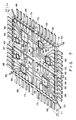
- Fig. 7 illustrates an MCP (multi chip package) to which the semiconductor chip shown in Fig. 3 is applied.
- semiconductor chips 55-61 are properly arranged and die-bonded onto beds 51-54 of lead frames fixed by hanging pins 50.
- Printed circuit boards 62-65 are formed on beds 51-54 so as to surround the semiconductor chips.
- a desired wiring pattern is formed on each of printed circuit boards 62-65 and used to electrically connect lead 66 and each of chips 55-61, which cannot be made close to each other any more in view of processing dimensions, and to connect chips 55-61 to one another.
- a plurality of I/O electrode pads 67 formed on the surface of each of chips 55-61 is connected by bonding wires 69 to connecting terminals 68 of the wiring patterns, which are near the semiconductor chips.
- the connecting terminals of the wiring patterns which are near the periphery of one of printed circuit boards 62-65, are connected to the wiring patterns of other printed circuit boards and electrically connected to leads 66.
- the former connection is performed by bonding wires 70
- the latter connection is performed by TAB tapes 71 using the TAB technique.
- TAB tape 71 is obtained by forming lead line 73 plated with copper on polyamide film 72 so as to correspond to lead 66.
- the connecting terminals of each of printed circuit boards 62-65 are connected to their corresponding leads 66 at once.
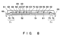
- Fig. 8 is a cross sectional view of the MCP shown in Fig. 7 which is sealed with resin.
- the printed circuit boards are connected to each other by bonding wires, and the semiconductor chips are connected to printed circuit boards by bonding wires.
- the printed circuit boards are connected to their corresponding leads 66 by TAB tapes 71.
- the MCP is thus sealed with mold resin 81.
- no bumps need to be formed, so that the manufacturing cost is not so increased, and an MCP of a multi-pin structure having a great large number of leads 66 is improved in reliability and productivity.
- a resin sealing type semiconductor device whose price is low and reliability is high can be provided, and an MCP can be improved in reliability and productivity.
Landscapes
- Wire Bonding (AREA)
- Lead Frames For Integrated Circuits (AREA)
- Encapsulation Of And Coatings For Semiconductor Or Solid State Devices (AREA)
- Structures Or Materials For Encapsulating Or Coating Semiconductor Devices Or Solid State Devices (AREA)
Applications Claiming Priority (6)
| Application Number | Priority Date | Filing Date | Title |
|---|---|---|---|
| JP21940489 | 1989-08-25 | ||
| JP219404/89 | 1989-08-25 | ||
| JP21940489 | 1989-08-25 | ||
| JP173065/90 | 1990-06-29 | ||
| JP2173065A JPH0777256B2 (ja) | 1989-08-25 | 1990-06-29 | 樹脂封止型半導体装置 |
| JP17306590 | 1990-06-29 |
Publications (3)
| Publication Number | Publication Date |
|---|---|
| EP0414257A2 true EP0414257A2 (de) | 1991-02-27 |
| EP0414257A3 EP0414257A3 (en) | 1991-07-31 |
| EP0414257B1 EP0414257B1 (de) | 2003-10-15 |
Family
ID=26495191
Family Applications (1)
| Application Number | Title | Priority Date | Filing Date |
|---|---|---|---|
| EP90116251A Expired - Lifetime EP0414257B1 (de) | 1989-08-25 | 1990-08-24 | Halbleiteranordnung des Harzverkapselungstyps, in dem ein sehr kleiner Halbleiterchip mit Harz versiegelt ist |
Country Status (5)
| Country | Link |
|---|---|
| EP (1) | EP0414257B1 (de) |
| JP (1) | JPH0777256B2 (de) |
| DE (1) | DE69034110T2 (de) |
| MY (1) | MY106858A (de) |
| SG (1) | SG67890A1 (de) |
Cited By (3)
| Publication number | Priority date | Publication date | Assignee | Title |
|---|---|---|---|---|
| EP0498446A3 (en) * | 1991-02-08 | 1993-10-20 | Toshiba Kk | Multichip packaged semiconductor device and method for manufacturing the same |
| US5701028A (en) * | 1994-07-18 | 1997-12-23 | Fujitsu Limited | Semiconductor device having tab leads |
| US20110260304A1 (en) * | 2008-10-13 | 2011-10-27 | Tyco Electronics Amp Gmbh | Leadframe for electronic components |
Families Citing this family (1)
| Publication number | Priority date | Publication date | Assignee | Title |
|---|---|---|---|---|
| JP7179712B2 (ja) * | 2019-12-26 | 2022-11-29 | 株式会社東芝 | ディスク装置 |
Family Cites Families (8)
| Publication number | Priority date | Publication date | Assignee | Title |
|---|---|---|---|---|
| JPS61183936A (ja) * | 1985-02-08 | 1986-08-16 | Toshiba Corp | 半導体装置 |
| JPS62226649A (ja) * | 1986-03-28 | 1987-10-05 | Toshiba Corp | ハイブリツド型半導体装置 |
| US4754317A (en) * | 1986-04-28 | 1988-06-28 | Monolithic Memories, Inc. | Integrated circuit die-to-lead frame interconnection assembly and method |
| US4774635A (en) * | 1986-05-27 | 1988-09-27 | American Telephone And Telegraph Company At&T Bell Laboratories | Semiconductor package with high density I/O lead connection |
| JPH0666354B2 (ja) * | 1986-07-29 | 1994-08-24 | 日本電気株式会社 | 半導体装置 |
| JPS6387846U (de) * | 1986-11-27 | 1988-06-08 | ||
| US4800419A (en) * | 1987-01-28 | 1989-01-24 | Lsi Logic Corporation | Support assembly for integrated circuits |
| US4994895A (en) * | 1988-07-11 | 1991-02-19 | Fujitsu Limited | Hybrid integrated circuit package structure |
-
1990
- 1990-06-29 JP JP2173065A patent/JPH0777256B2/ja not_active Expired - Fee Related
- 1990-08-21 MY MYPI90001403A patent/MY106858A/en unknown
- 1990-08-24 DE DE69034110T patent/DE69034110T2/de not_active Expired - Fee Related
- 1990-08-24 EP EP90116251A patent/EP0414257B1/de not_active Expired - Lifetime
- 1990-08-24 SG SG1996002863A patent/SG67890A1/en unknown
Cited By (3)
| Publication number | Priority date | Publication date | Assignee | Title |
|---|---|---|---|---|
| EP0498446A3 (en) * | 1991-02-08 | 1993-10-20 | Toshiba Kk | Multichip packaged semiconductor device and method for manufacturing the same |
| US5701028A (en) * | 1994-07-18 | 1997-12-23 | Fujitsu Limited | Semiconductor device having tab leads |
| US20110260304A1 (en) * | 2008-10-13 | 2011-10-27 | Tyco Electronics Amp Gmbh | Leadframe for electronic components |
Also Published As
| Publication number | Publication date |
|---|---|
| DE69034110T2 (de) | 2004-07-15 |
| JPH0777256B2 (ja) | 1995-08-16 |
| EP0414257B1 (de) | 2003-10-15 |
| MY106858A (en) | 1995-08-30 |
| JPH03163858A (ja) | 1991-07-15 |
| DE69034110D1 (de) | 2003-11-20 |
| SG67890A1 (en) | 1999-10-19 |
| EP0414257A3 (en) | 1991-07-31 |
Similar Documents
| Publication | Publication Date | Title |
|---|---|---|
| US6121070A (en) | Flip chip down-bond: method and apparatus | |
| US6265766B1 (en) | Flip chip adaptor package for bare die | |
| US7595551B2 (en) | Semiconductor package for a large die | |
| CN101421833B (zh) | 封装集成电路小片的方法 | |
| JP2895022B2 (ja) | チップスケールパッケージの製造方法 | |
| US6642082B2 (en) | Method for manufacturing a resin-sealed semiconductor device | |
| EP0623954B1 (de) | Vergossene Kunststoffverkapselung für elektronische Anordnungen | |
| US5196992A (en) | Resin sealing type semiconductor device in which a very small semiconductor chip is sealed in package with resin | |
| US8030766B2 (en) | Semiconductor device | |
| US5382546A (en) | Semiconductor device and method of fabricating same, as well as lead frame used therein and method of fabricating same | |
| US5559305A (en) | Semiconductor package having adjacently arranged semiconductor chips | |
| EP0414257A2 (de) | Halbleiteranordnung des Harzverkapselungstyps, in dem ein sehr kleiner Halbleiterchip mit Harz versiegelt ist | |
| US6628136B2 (en) | Method and apparatus for testing a semiconductor package | |
| JP4038021B2 (ja) | 半導体装置の製造方法 | |
| JPH10154768A (ja) | 半導体装置及びその製造方法 | |
| KR100235107B1 (ko) | 탭 패키지 | |
| EP0727819A2 (de) | Aufgestapelte Halbleiteranordnung und Verfahren zu ihrer Herstellung | |
| JP2885202B2 (ja) | 半導体パッケージ用検査治具 | |
| JP3398556B2 (ja) | 半導体装置の製造方法 | |
| JP3024046B2 (ja) | 半導体パッケージ | |
| JP2992408B2 (ja) | Icパッケージとその実装構造 | |
| JPH1174302A (ja) | 樹脂封止型半導体装置 | |
| KR930011117B1 (ko) | 반도체 패키지 및 그 실장방법 | |
| KR950003906B1 (ko) | 탭 패키지 | |
| JPH1022329A (ja) | 半導体装置 |
Legal Events
| Date | Code | Title | Description |
|---|---|---|---|
| PUAI | Public reference made under article 153(3) epc to a published international application that has entered the european phase |
Free format text: ORIGINAL CODE: 0009012 |
|
| 17P | Request for examination filed |
Effective date: 19900824 |
|
| AK | Designated contracting states |
Kind code of ref document: A2 Designated state(s): DE FR GB |
|
| PUAL | Search report despatched |
Free format text: ORIGINAL CODE: 0009013 |
|
| RHK1 | Main classification (correction) |
Ipc: H01L 23/495 |
|
| AK | Designated contracting states |
Kind code of ref document: A3 Designated state(s): DE FR GB |
|
| 17Q | First examination report despatched |
Effective date: 19930611 |
|
| APAB | Appeal dossier modified |
Free format text: ORIGINAL CODE: EPIDOS NOAPE |
|
| APAD | Appeal reference recorded |
Free format text: ORIGINAL CODE: EPIDOS REFNE |
|
| APAD | Appeal reference recorded |
Free format text: ORIGINAL CODE: EPIDOS REFNE |
|
| APAB | Appeal dossier modified |
Free format text: ORIGINAL CODE: EPIDOS NOAPE |
|
| GRAG | Despatch of communication of intention to grant |
Free format text: ORIGINAL CODE: EPIDOS AGRA |
|
| GRAH | Despatch of communication of intention to grant a patent |
Free format text: ORIGINAL CODE: EPIDOS IGRA |
|
| GRAH | Despatch of communication of intention to grant a patent |
Free format text: ORIGINAL CODE: EPIDOS IGRA |
|
| GRAA | (expected) grant |
Free format text: ORIGINAL CODE: 0009210 |
|
| AK | Designated contracting states |
Kind code of ref document: B1 Designated state(s): DE FR GB |
|
| REG | Reference to a national code |
Ref country code: GB Ref legal event code: FG4D |
|
| REF | Corresponds to: |
Ref document number: 69034110 Country of ref document: DE Date of ref document: 20031120 Kind code of ref document: P |
|
| ET | Fr: translation filed | ||
| PLBE | No opposition filed within time limit |
Free format text: ORIGINAL CODE: 0009261 |
|
| STAA | Information on the status of an ep patent application or granted ep patent |
Free format text: STATUS: NO OPPOSITION FILED WITHIN TIME LIMIT |
|
| 26N | No opposition filed |
Effective date: 20040716 |
|
| PGFP | Annual fee paid to national office [announced via postgrant information from national office to epo] |
Ref country code: GB Payment date: 20050824 Year of fee payment: 16 |
|
| APAH | Appeal reference modified |
Free format text: ORIGINAL CODE: EPIDOSCREFNO |
|
| PGFP | Annual fee paid to national office [announced via postgrant information from national office to epo] |
Ref country code: FR Payment date: 20060808 Year of fee payment: 17 |
|
| PGFP | Annual fee paid to national office [announced via postgrant information from national office to epo] |
Ref country code: DE Payment date: 20060817 Year of fee payment: 17 |
|
| GBPC | Gb: european patent ceased through non-payment of renewal fee |
Effective date: 20060824 |
|
| PG25 | Lapsed in a contracting state [announced via postgrant information from national office to epo] |
Ref country code: GB Free format text: LAPSE BECAUSE OF NON-PAYMENT OF DUE FEES Effective date: 20060824 |
|
| REG | Reference to a national code |
Ref country code: FR Ref legal event code: ST Effective date: 20080430 |
|
| PG25 | Lapsed in a contracting state [announced via postgrant information from national office to epo] |
Ref country code: DE Free format text: LAPSE BECAUSE OF NON-PAYMENT OF DUE FEES Effective date: 20080301 |
|
| PG25 | Lapsed in a contracting state [announced via postgrant information from national office to epo] |
Ref country code: FR Free format text: LAPSE BECAUSE OF NON-PAYMENT OF DUE FEES Effective date: 20070831 |