EP0414393A1 - Connecteurs électriques - Google Patents
Connecteurs électriques Download PDFInfo
- Publication number
- EP0414393A1 EP0414393A1 EP90308484A EP90308484A EP0414393A1 EP 0414393 A1 EP0414393 A1 EP 0414393A1 EP 90308484 A EP90308484 A EP 90308484A EP 90308484 A EP90308484 A EP 90308484A EP 0414393 A1 EP0414393 A1 EP 0414393A1
- Authority
- EP
- European Patent Office
- Prior art keywords
- board
- contact
- contact pads
- edge connector
- connector
- Prior art date
- Legal status (The legal status is an assumption and is not a legal conclusion. Google has not performed a legal analysis and makes no representation as to the accuracy of the status listed.)
- Withdrawn
Links
Images


Classifications
-
- H—ELECTRICITY
- H01—ELECTRIC ELEMENTS
- H01R—ELECTRICALLY-CONDUCTIVE CONNECTIONS; STRUCTURAL ASSOCIATIONS OF A PLURALITY OF MUTUALLY-INSULATED ELECTRICAL CONNECTING ELEMENTS; COUPLING DEVICES; CURRENT COLLECTORS
- H01R12/00—Structural associations of a plurality of mutually-insulated electrical connecting elements, specially adapted for printed circuits, e.g. printed circuit boards [PCB], flat or ribbon cables, or like generally planar structures, e.g. terminal strips, terminal blocks; Coupling devices specially adapted for printed circuits, flat or ribbon cables, or like generally planar structures; Terminals specially adapted for contact with, or insertion into, printed circuits, flat or ribbon cables, or like generally planar structures
- H01R12/50—Fixed connections
- H01R12/51—Fixed connections for rigid printed circuits or like structures
- H01R12/55—Fixed connections for rigid printed circuits or like structures characterised by the terminals
- H01R12/57—Fixed connections for rigid printed circuits or like structures characterised by the terminals surface mounting terminals
-
- H—ELECTRICITY
- H01—ELECTRIC ELEMENTS
- H01R—ELECTRICALLY-CONDUCTIVE CONNECTIONS; STRUCTURAL ASSOCIATIONS OF A PLURALITY OF MUTUALLY-INSULATED ELECTRICAL CONNECTING ELEMENTS; COUPLING DEVICES; CURRENT COLLECTORS
- H01R12/00—Structural associations of a plurality of mutually-insulated electrical connecting elements, specially adapted for printed circuits, e.g. printed circuit boards [PCB], flat or ribbon cables, or like generally planar structures, e.g. terminal strips, terminal blocks; Coupling devices specially adapted for printed circuits, flat or ribbon cables, or like generally planar structures; Terminals specially adapted for contact with, or insertion into, printed circuits, flat or ribbon cables, or like generally planar structures
- H01R12/70—Coupling devices
- H01R12/71—Coupling devices for rigid printing circuits or like structures
- H01R12/72—Coupling devices for rigid printing circuits or like structures coupling with the edge of the rigid printed circuits or like structures
- H01R12/721—Coupling devices for rigid printing circuits or like structures coupling with the edge of the rigid printed circuits or like structures cooperating directly with the edge of the rigid printed circuits
-
- H—ELECTRICITY
- H05—ELECTRIC TECHNIQUES NOT OTHERWISE PROVIDED FOR
- H05K—PRINTED CIRCUITS; CASINGS OR CONSTRUCTIONAL DETAILS OF ELECTRIC APPARATUS; MANUFACTURE OF ASSEMBLAGES OF ELECTRICAL COMPONENTS
- H05K1/00—Printed circuits
- H05K1/02—Details
- H05K1/11—Printed elements for providing electric connections to or between printed circuits
- H05K1/117—Pads along the edge of rigid circuit boards, e.g. for pluggable connectors
-
- H—ELECTRICITY
- H05—ELECTRIC TECHNIQUES NOT OTHERWISE PROVIDED FOR
- H05K—PRINTED CIRCUITS; CASINGS OR CONSTRUCTIONAL DETAILS OF ELECTRIC APPARATUS; MANUFACTURE OF ASSEMBLAGES OF ELECTRICAL COMPONENTS
- H05K3/00—Apparatus or processes for manufacturing printed circuits
- H05K3/40—Forming printed elements for providing electric connections to or between printed circuits
- H05K3/4007—Surface contacts, e.g. bumps
- H05K3/4015—Surface contacts, e.g. bumps using auxiliary conductive elements, e.g. pieces of metal foil, metallic spheres
-
- H—ELECTRICITY
- H05—ELECTRIC TECHNIQUES NOT OTHERWISE PROVIDED FOR
- H05K—PRINTED CIRCUITS; CASINGS OR CONSTRUCTIONAL DETAILS OF ELECTRIC APPARATUS; MANUFACTURE OF ASSEMBLAGES OF ELECTRICAL COMPONENTS
- H05K2201/00—Indexing scheme relating to printed circuits covered by H05K1/00
- H05K2201/03—Conductive materials
- H05K2201/0332—Structure of the conductor
- H05K2201/0364—Conductor shape
- H05K2201/0367—Metallic bump or raised conductor not used as solder bump
-
- H—ELECTRICITY
- H05—ELECTRIC TECHNIQUES NOT OTHERWISE PROVIDED FOR
- H05K—PRINTED CIRCUITS; CASINGS OR CONSTRUCTIONAL DETAILS OF ELECTRIC APPARATUS; MANUFACTURE OF ASSEMBLAGES OF ELECTRICAL COMPONENTS
- H05K2201/00—Indexing scheme relating to printed circuits covered by H05K1/00
- H05K2201/09—Shape and layout
- H05K2201/09209—Shape and layout details of conductors
- H05K2201/09372—Pads and lands
- H05K2201/0939—Curved pads, e.g. semi-circular or elliptical pads or lands
-
- H—ELECTRICITY
- H05—ELECTRIC TECHNIQUES NOT OTHERWISE PROVIDED FOR
- H05K—PRINTED CIRCUITS; CASINGS OR CONSTRUCTIONAL DETAILS OF ELECTRIC APPARATUS; MANUFACTURE OF ASSEMBLAGES OF ELECTRICAL COMPONENTS
- H05K2201/00—Indexing scheme relating to printed circuits covered by H05K1/00
- H05K2201/09—Shape and layout
- H05K2201/09209—Shape and layout details of conductors
- H05K2201/09654—Shape and layout details of conductors covering at least two types of conductors provided for in H05K2201/09218 - H05K2201/095
- H05K2201/09709—Staggered pads, lands or terminals; Parallel conductors in different planes
-
- H—ELECTRICITY
- H05—ELECTRIC TECHNIQUES NOT OTHERWISE PROVIDED FOR
- H05K—PRINTED CIRCUITS; CASINGS OR CONSTRUCTIONAL DETAILS OF ELECTRIC APPARATUS; MANUFACTURE OF ASSEMBLAGES OF ELECTRICAL COMPONENTS
- H05K2201/00—Indexing scheme relating to printed circuits covered by H05K1/00
- H05K2201/10—Details of components or other objects attached to or integrated in a printed circuit board
- H05K2201/10613—Details of electrical connections of non-printed components, e.g. special leads
- H05K2201/10742—Details of leads
- H05K2201/1075—Shape details
- H05K2201/10863—Adaptations of leads or holes for facilitating insertion
-
- H—ELECTRICITY
- H05—ELECTRIC TECHNIQUES NOT OTHERWISE PROVIDED FOR
- H05K—PRINTED CIRCUITS; CASINGS OR CONSTRUCTIONAL DETAILS OF ELECTRIC APPARATUS; MANUFACTURE OF ASSEMBLAGES OF ELECTRICAL COMPONENTS
- H05K3/00—Apparatus or processes for manufacturing printed circuits
- H05K3/30—Assembling printed circuits with electric components, e.g. with resistors
- H05K3/32—Assembling printed circuits with electric components, e.g. with resistors electrically connecting electric components or wires to printed circuits
- H05K3/325—Assembling printed circuits with electric components, e.g. with resistors electrically connecting electric components or wires to printed circuits by abutting or pinching; Mechanical auxiliary parts therefor
-
- H—ELECTRICITY
- H05—ELECTRIC TECHNIQUES NOT OTHERWISE PROVIDED FOR
- H05K—PRINTED CIRCUITS; CASINGS OR CONSTRUCTIONAL DETAILS OF ELECTRIC APPARATUS; MANUFACTURE OF ASSEMBLAGES OF ELECTRICAL COMPONENTS
- H05K3/00—Apparatus or processes for manufacturing printed circuits
- H05K3/30—Assembling printed circuits with electric components, e.g. with resistors
- H05K3/32—Assembling printed circuits with electric components, e.g. with resistors electrically connecting electric components or wires to printed circuits
- H05K3/34—Assembling printed circuits with electric components, e.g. with resistors electrically connecting electric components or wires to printed circuits by soldering
- H05K3/341—Surface mounted components
-
- Y—GENERAL TAGGING OF NEW TECHNOLOGICAL DEVELOPMENTS; GENERAL TAGGING OF CROSS-SECTIONAL TECHNOLOGIES SPANNING OVER SEVERAL SECTIONS OF THE IPC; TECHNICAL SUBJECTS COVERED BY FORMER USPC CROSS-REFERENCE ART COLLECTIONS [XRACs] AND DIGESTS
- Y10—TECHNICAL SUBJECTS COVERED BY FORMER USPC
- Y10S—TECHNICAL SUBJECTS COVERED BY FORMER USPC CROSS-REFERENCE ART COLLECTIONS [XRACs] AND DIGESTS
- Y10S439/00—Electrical connectors
- Y10S439/951—PCB having detailed leading edge
Definitions
- This invention relates to electrical connectors and relates more specifically to electrical edge connectors for making electrical connections to printed circuit or wiring boards by the engagement of spring contacts of the edge connector with contact elements provided on the printed circuit boards.
- the contact elements referred conventionally comprise a group of thin conductive strips extending in parallel relationship from the edge of the printed circuit board. It is common practice to plate these conductive strips and those parts of the spring contacts of the edge connector which make contact therewith with precious metal (e.g. gold) in order to avoid contact oxidation problems.
- precious metal e.g. gold
- the present invention is directed to further improvements in the contact pad arrangement disclosed in the above-mentioned patent.
- an electrical connecting arrangement between a printed circuit/wiring board and an edge connector having an insulating body accommodating a plurality of spring contacts for making contact with contact elements located on the printed circuit/wiring board, in which the contact elements on the printed circuit/wiring board define contact pads which are spaced from an edge of the board adapted for insertion into the edge connector and which are formed with a convex profile at least in the direction of insertion of the board into the edge connector and in which the depth of an opening in the connector for receiving the board edge and the distance of the contact pads from the board edge is such that during insertion of the board into the connector the contact springs ride up and over the convex profile and come to rest on a part of the contact pad beyond the centre line of the convex profile when the board is fully inserted.
- the connecting arrangement according to the above aspect of the present invention not only is the aforesaid scuffing of the spring contact plating material by engagement with the sharp edges of the contact strips of the circuit board avoided but the mutual areas of contact pressure engagement between the spring contacts and the contact pads on the printed circuit board when the edge connector is fully engaged with the board are areas which are not subjected to wear during insertion and withdrawal of the board from the edge connector. Moreover, the spring forces exerted on the contact pads by the edge connector spring contacts tend to produce accelerated movement of the printed circuit board into the edge connector as the spring contacts move beyond the centre lines of the convex profiles of the contact pads. This feature not only has the advantage of assisting full engagement between the edge connector and the circuit board but it may be utilised to provide a positive snap action connection between the board and the connector, thereby positively eliminating any uncertainty as to whether the board and connector are fully engaged.
- the spring contacts are shaped so that the angle of the spring contact part that first makes contact with a contact pad is less steeply inclined relative to the direction of insertion of the board into the edge connector than is that part of the spring contact which finally comes to rest on the contact pad. This feature provides for ease of full insertion of the board into the edge connector whilst producing higher board retention forces.
- ' are preferably dome-shaped thereby providing optimum Hertz stress but other configurations of contact pad may be utilised without departing from the principle or spirit of the invention.
- they may be semi-cylindrical or the pads may have a tapered/inclined foremost section and a generally semi-cylindrical rearmost end.
- the spring contacts and/or contact pads may be gold plated over those parts which make pressure engagement or the contacts may be plated with a tin alloy, for example.
- an electrical edge connector for receiving a printed circuit or wiring board comprises an insulating body with a board-receiving opening therein which contains an abutment for engagement by the board edge when fully inserted into the connector, in which the abutment is adapted to restrain the board against movement thereof in directions other than that of withdrawal from the connector in order to provide a highly stable connector/board assembly thereby preventing relative movement between the usual co-operating contacts of the edge connector and board when the latter are in full engagement.
- the abutment may be provided with a groove or channel which receives the edge of the board, the groove or channel being V-shaped or semi-cylindrical, for example.
- the stability of the assembly may be further enhanced by spacing the contact pads further from the board edge than would otherwise be necessary.
- a third aspect of the present invention there is provided a method of attaching contact pads having a curved profile to a printed circuit board, preferably at positions relative to the edge of the printed circuit board facilitating the provision of the electrical connecting arrangement according to the first aspect of this invention, in which the printed circuit board is provided with a plurality of conductive regions to which conductive bonding material is applied at positions at which the contact pads are to be secured to the board and in which the contact pads are accurately positioned relative to the conductive areas and the bonded material is melted or otherwise activated and caused to become re-solidified to cause bonding of the contact pads to the printed circuit board.
- a printed circuit board provided with contact pads according to this third aspect of the present invention may also be used with the edge connector constructed in accordance with the second aspect of this invention.
- the bonding material may comprise solder paste which may, in the case of miniaturised surface mounted boards be applied to the conductive regions of the board by silk screening.
- solder paste which may, in the case of miniaturised surface mounted boards be applied to the conductive regions of the board by silk screening.
- the adhesion of such contact pads to the boards will be appreciably better than that between the conventional contact strips provided at the edge of the board in the case of the previously described conventional printed board/edge connector arrangement.
- the contact pads may be produced simply by pressing or stamping the pads from a sheet of suitable material (e.g. phosphor bronze).
- suitable material e.g. phosphor bronze
- the action of the press tool may itself produce a sufficiently convex profile for the contact pads in the case of dome-shaped pads.
- the general base shape of the contact pads may be circular or rectangular and in the case when solder (e.g. solder paste) is used as the bonding material the precise location of the pads on the underlying conductive regions of the board which will be of corresponding shape and dimensions will be achieved by solder re-flow alignment resulting from the surface tension produced in the molten solder during the solder re-flow procedure.
- solder e.g. solder paste
- the positioning of the contact pads on the printed circuit boards may conveniently be achieved by the use of a "pick and place” mechanism conventionally used in surface mounting technology for the positioning of components on the board prior to bonding thereof to the board.
- the contact pads may be provided on one or both sides of the printed circuit board according to the spring contact arrangement of the edge connector.
- the contact pads may also be arranged in a single row on one or both sides of the board at a predetermined distance from the edge of the board or a plurality of rows may effectively be provided on one or both sides of the board by staggering alternate contact pads in the direction of engagement of the board with the edge connector. With this staggered contact pad arrangement the tracking distance between adjacent contacts is increased.
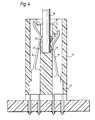
- this shows an edge connector 1 the insulating body of which is shown in cross section at 2 having accommodated within internal cavities along the length of the body a multiplicity of spring contacts, such as the spring contacts 3 and 4.
- the spring contacts of the edge connector are arranged in two sets for co-operating with contacts, such as the contacts 5 and 6, provided on the respective sides of a printed circuit board 7.
- the edge connector could alternatively be provided with a single set of spring contacts for co-operation with contact pads provided on one side only of the printed circuit board.
- the edge connector is mounted on a circuit board 8 (e.g. back-plane assembly board) by the soldering of the spring contacts 3 and 4 to conductive channels of the board 8.
- the contact pads 5 and 6 will be contained within rows of contact pads provided on opposite sides of the board 7 and accurately spaced in from the edge of the board 7.
- the contact pads such as the contact pads 5 and 6, have a convex profile in the direction of insertion of the board 7 into the edge connector 1.
- the contact pads 5 and 6 which are preferably dome-shaped are first engaged by the curved sections 9 and 10 of the spring contacts 5 and 6 at about the small areas or points 11 and 12 on the contact pads thereby concentrating the spring contact pressure exerted by the spring contacts at the points of mutual engagement between the contacts to provide optimum Hertz stress at these points.
- the spring contacts 3 and 4 ride over the spherical surface of the contact pads 5 and 6 the points of mutual engagement between the contacts will constantly be changing thereby distributing any contact wear over a series of points of mutual engagement.
- This spring force exerted on the contact pads by the spring contact not only provides the requisite electrical connection but also acts in a direction to preserve full engagement between the edge connector 1 and the board 7. This would help to avoid so-called “fretting corrosion” if tin alloy plated contacts were used on the board and/or edge connector.
- the profile of the dome-shaped contacts also tends to prevent the build up of any oxide or other debris which may otherwise be shifted forward to the contact rest position by the spring contacts during insertion of the board into the edge connector.
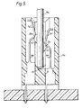
- FIGS 2 and 3 of the drawings show preferred embodiments of the invention in which spring contacts 3a and 4a of the edge connector 1a having an insulating body 2a have free end portions "b" thereof which are less steeply inclined relative to the direction of insertion of the board 7a into the edge connector than the spring contact portions "c".
- This arrangement provides for ease of insertion of the board 7a into the edge connector as the less steeply inclined portions "b" of the springs 3a and 4a ride up and over the convex profiles of the respective dome-shaped contact pads 5a and 6a.
- the body 2a of the edge connector is provided with an abutment 30 which is provided with a V-shaped groove 31 in the case of Figure 2 and a semi-cylindrical groove or channel 32 in the case of Figure 3.
- the groove 31 or 32 receives the end of the printed circuit board 7a and serves to restrain the board 7a against lateral movement, thereby preventing relative movement between the connector contacts 3a and 4a and the co-operating board contact pads 5a and 6a under small amplitude vibration conditions which could cause fretting corrosion as previously mentioned.
- the stability of the arrangement is also enhanced by positioning the contact pads 5 and 6 farther from the edge of the board than in the Figure 1 arrangement.
- FIG. 4 of the drawings shows an edge connector 15 with a printed circuit board 16 inserted therein in which the connector has an insulating body 17 accommodating along its length two sets of spring contacts containing contacts such as the contacts 18 and 19, the positions of alternate spring contacts being staggered relative to the board receiving end of the connector 15.
- the board 16 in this case is provided on both sides with rows of contact pads alternate pads of which such as the pads 20 and 21 and the pads 22 and 23 are staggered correspondingly to the staggering of the spring contacts 18 and 19.
- This arrangement increases the tracking area between adjacent contacts but in other respects the operation is as fully described with reference to Figure 1 of the drawings.
- the staggered arrangement of the contact pads can readily be appreciated by reference to Figures 7(c) and 7(d).
- the body 17a of the connector has an abutment 33 which is provided with a semi-cylindrical groove 34 for receiving the end of the printed board 16a to provide a highly stable assembly as fully described with reference to Figures 2 and 3.
- this shows a dome-shaped pad 24 and alternative forms of convex profile contact pads 25 and 26 which could be substituted for the dome-shaped pads of Figures 1 to 5.
- the semi-cylindrical pad 25 may be used or the pad 26 which has a leading tapered inclined section 27 and a rearmost semi-cylindrical section 28.
- contact pads having a convex profile such as the dome shaped pad 24 the semi-cylindrical pad 25 or the contact pad 26 having a tapered foremost end followed by a semi-cylindrical tail section as shown in Figure 6 may be attached to a printed circuit board by applying solder paste to conductive regions of corresponding shape and corresponding dimensions to the bases of the contact pads. These conductive regions will normally be produced on the board by conventional etching techniques.
- the solder paste may be applied to the board using silk screening processes after which the contact pads may be positioned on the solder paste to which they will adhere at appropriate locations as by the use of so-called pick and place mechanisms commonly used in surface mounting technology for component positioning purposes.
- solder paste After approximate positioning of the contact pads on the board the solder paste will be melted using solder reflow techniques whereby the surface tension of the molten solder will produce self alignment of the contact pads with respect to the correspondingly shaped correspondingly dimensioned conductive regions on the board for the precise positioning of the contact pads relative to the board.
- Boards having contact pads secured thereto in the manner just above described are eminently suitable for use in the board/edge connector electrical connector arrangement according to the first-mentioned aspect of the present invention.
- the present invention provides an advantageous edge connector/printed circuit board connecting arrangement as well as an improved arrangement for the positioning and attachment of contact pads to a printed circuit board which is eminently suitable for use in the aforesaid advantageous board/edge connector connecting arrangement.
Landscapes
- Engineering & Computer Science (AREA)
- Microelectronics & Electronic Packaging (AREA)
- Manufacturing & Machinery (AREA)
- Coupling Device And Connection With Printed Circuit (AREA)
Applications Claiming Priority (2)
| Application Number | Priority Date | Filing Date | Title |
|---|---|---|---|
| GB8919167 | 1989-08-23 | ||
| GB8919167A GB2236217A (en) | 1989-08-23 | 1989-08-23 | Improvement relating to electrical connectors |
Publications (1)
| Publication Number | Publication Date |
|---|---|
| EP0414393A1 true EP0414393A1 (fr) | 1991-02-27 |
Family
ID=10662008
Family Applications (1)
| Application Number | Title | Priority Date | Filing Date |
|---|---|---|---|
| EP90308484A Withdrawn EP0414393A1 (fr) | 1989-08-23 | 1990-08-01 | Connecteurs électriques |
Country Status (3)
| Country | Link |
|---|---|
| US (1) | US5037315A (fr) |
| EP (1) | EP0414393A1 (fr) |
| GB (1) | GB2236217A (fr) |
Cited By (3)
| Publication number | Priority date | Publication date | Assignee | Title |
|---|---|---|---|---|
| WO1997022163A1 (fr) * | 1995-12-11 | 1997-06-19 | The Whitaker Corporation | Connecteur de carte enfichable pour plaquette de circuit imprime |
| EP0880203A2 (fr) * | 1997-05-20 | 1998-11-25 | Framatome Connectors International | Connecteur de bordure de carte avec des contacts flexibles à ressort recourbes en forme similaire avec des surfaces de contact à plusieurs niveaux |
| WO2012012360A1 (fr) * | 2010-07-21 | 2012-01-26 | 3M Innovative Properties Company | Cartes de circuit imprimé pour modules de télécommunication |
Families Citing this family (19)
| Publication number | Priority date | Publication date | Assignee | Title |
|---|---|---|---|---|
| DE19650154C2 (de) * | 1996-12-04 | 1999-06-10 | Lemfoerder Metallwaren Ag | Schaltvorrichtung für ein Getriebe eines KFZ mit einer mit Sensoren, Leuchtdioden, Prozessen und anderen elektronischen Bauelementen bestückten Leiterplatte und Verfahren zur Herstellung einer gekrümmten Leiterplatte zur Verwendung in einer solchen Schaltvorrichtung |
| JP2000113920A (ja) * | 1998-10-01 | 2000-04-21 | Mitsubishi Electric Corp | モジュール |
| TW388572U (en) * | 1998-12-22 | 2000-04-21 | Hon Hai Prec Ind Co Ltd | Electrical connector |
| DE10317286B3 (de) * | 2003-04-09 | 2004-10-07 | Nicolay Verwaltungs-Gmbh | Vorrichtung zum elektrischen Verbinden einer Anschlußleitung mit einer Elektrode, insbesondere einer medizintechnischen Hautelektrode |
| TWM276354U (en) * | 2005-02-05 | 2005-09-21 | Egbn Electronics Ltd | Card edge connector |
| JP2006236657A (ja) * | 2005-02-23 | 2006-09-07 | Nec Corp | コネクタ装置 |
| TWM290311U (en) * | 2005-10-28 | 2006-05-01 | Chicony Electronics Co Ltd | Flexible PCB |
| TWM339185U (en) * | 2008-01-15 | 2008-08-21 | Wintek Corp | Bend prevention structure for connection terminal of FPC |
| WO2015073989A2 (fr) | 2013-11-17 | 2015-05-21 | Apple Inc. | Réceptacle de connecteur comportant une languette |
| WO2015073974A2 (fr) | 2013-11-17 | 2015-05-21 | Apple Inc. | Réceptacle de connecteur comportant un écran de protection |
| US9450339B2 (en) | 2014-01-12 | 2016-09-20 | Apple Inc. | Ground contacts for reduced-length connector inserts |
| US9490581B2 (en) | 2014-05-26 | 2016-11-08 | Apple Inc. | Connector insert assembly |
| US10418763B2 (en) | 2014-05-26 | 2019-09-17 | Apple Inc. | Connector insert assembly |
| US9356370B2 (en) | 2014-05-26 | 2016-05-31 | Apple Inc. | Interposer for connecting a receptacle tongue to a printed circuit board |
| US9515439B2 (en) | 2014-05-26 | 2016-12-06 | Apple Inc. | Connector insert assembly |
| US9564697B2 (en) | 2014-11-13 | 2017-02-07 | Lear Corporation | Press fit electrical terminal having a solder tab shorter than PCB thickness and method of using same |
| US11367974B1 (en) | 2021-06-14 | 2022-06-21 | Daniel R. Judd | ECG electrode connector |
| CN117202497B (zh) * | 2023-10-24 | 2024-05-28 | 百强电子(深圳)有限公司 | 一种具有压接结构的电路板及其制作方法 |
| KR20250088236A (ko) * | 2023-12-08 | 2025-06-17 | 삼성전자주식회사 | 메모리 모듈 및 이를 포함하는 전자 소자 어셈블리 |
Citations (3)
| Publication number | Priority date | Publication date | Assignee | Title |
|---|---|---|---|---|
| FR2460552A1 (fr) * | 1979-07-02 | 1981-01-23 | Bunker Ramo | Carte imprimee avec embout ogival rapporte |
| GB2179578A (en) * | 1985-08-23 | 1987-03-11 | Bicc Plc | Mounting electrical contacts |
| EP0250045A1 (fr) * | 1986-06-17 | 1987-12-23 | E.I. Du Pont De Nemours And Company | Méthode de montage de surfaces de contact revêtues de métal noble sur un substrat et substrat muni de telles surfaces de contact |
Family Cites Families (22)
| Publication number | Priority date | Publication date | Assignee | Title |
|---|---|---|---|---|
| GB615957A (en) * | 1942-11-07 | 1949-01-13 | Cinch Mfg Corp | Improvements in and relating to tube sockets and shield retainers for thermionic andlike tubes |
| DE1072672B (de) * | 1956-11-13 | 1960-01-07 | Amphenol Electronic Corporation, Chicago, IU. (V. St. A.) | Elektrische Steckverbindung mit isolierenden Kontakthaltern |
| US3015797A (en) * | 1958-10-28 | 1962-01-02 | United Carr Fastener Corp | Electrical connector with polarizing key |
| NL144121B (nl) * | 1965-09-23 | 1974-11-15 | Amp Inc | Elektrisch verbindingsstelsel voor het verbinden van een elektrische geleider met een insteekbaar bedrukt paneel. |
| US3537063A (en) * | 1968-06-17 | 1970-10-27 | Ibm | Circuit card connector |
| NL7905518A (nl) * | 1978-07-19 | 1980-01-22 | Matsushita Electric Ind Co Ltd | Werkwijze voor het monteren van elektronische delen. |
| US4266839A (en) * | 1979-07-06 | 1981-05-12 | E. I. Du Pont De Nemours And Company | Zero insertion force toggle link connector |
| GB2132538B (en) * | 1982-11-20 | 1986-05-08 | Int Computers Ltd | Method of soldering a conductive element to a conductor pad |
| US4468073A (en) * | 1983-03-21 | 1984-08-28 | Precision Connector Designs, Inc. | Zero insertion force connector |
| GB8310001D0 (en) * | 1983-04-13 | 1983-05-18 | Gen Electric Co Plc | Electrical connector assembly |
| US4480884A (en) * | 1983-07-01 | 1984-11-06 | International Business Machines Corporation | Zero insertion force connector and circuit card assembly |
| US4545610A (en) * | 1983-11-25 | 1985-10-08 | International Business Machines Corporation | Method for forming elongated solder connections between a semiconductor device and a supporting substrate |
| US4636021A (en) * | 1984-03-02 | 1987-01-13 | Amp Incorporated | High density ZIF card edge connector |
| GB2156153B (en) * | 1984-03-21 | 1988-02-24 | Pitney Bowes Inc | Alignment process for semiconductor chips |
| US4747794A (en) * | 1984-09-28 | 1988-05-31 | North American Specialties Corp. | Electrical connector |
| US4678250A (en) * | 1985-01-08 | 1987-07-07 | Methode Electronics, Inc. | Multi-pin electrical header |
| JPS625363U (fr) * | 1985-03-25 | 1987-01-13 | ||
| US4606594A (en) * | 1985-04-22 | 1986-08-19 | Amp Incorporated | ZIF connector with wipe |
| US4630874A (en) * | 1985-06-20 | 1986-12-23 | Amp Incorporated | Zero insertion force electrical interconnection assembly |
| GB8522429D0 (en) * | 1985-09-10 | 1985-10-16 | Plessey Co Plc | Alignment for hybrid device |
| US4761881A (en) * | 1986-09-15 | 1988-08-09 | International Business Machines Corporation | Single step solder process |
| US4872851A (en) * | 1989-02-27 | 1989-10-10 | International Business Machines Corp. | Electrical connector with torsional contacts |
-
1989
- 1989-08-23 GB GB8919167A patent/GB2236217A/en not_active Withdrawn
-
1990
- 1990-08-01 EP EP90308484A patent/EP0414393A1/fr not_active Withdrawn
- 1990-08-13 US US07/566,632 patent/US5037315A/en not_active Expired - Fee Related
Patent Citations (3)
| Publication number | Priority date | Publication date | Assignee | Title |
|---|---|---|---|---|
| FR2460552A1 (fr) * | 1979-07-02 | 1981-01-23 | Bunker Ramo | Carte imprimee avec embout ogival rapporte |
| GB2179578A (en) * | 1985-08-23 | 1987-03-11 | Bicc Plc | Mounting electrical contacts |
| EP0250045A1 (fr) * | 1986-06-17 | 1987-12-23 | E.I. Du Pont De Nemours And Company | Méthode de montage de surfaces de contact revêtues de métal noble sur un substrat et substrat muni de telles surfaces de contact |
Non-Patent Citations (2)
| Title |
|---|
| FEINWERKTECHNIK + MESSTECHNIK. no. 5, July 87, MÜNCHEN DE pages 323 - 324; CZESCHKA ET AL.: "STECKVERBINDER FÜR OBERFLÄCHENMONTAGE (SMT)" * |
| IBM TECHNICAL DISCLOSURE BULLETIN. vol. 25, no. 3B, August 82, NEW YORK US pages 1410 - 1411; CHIRINO ET AL.: "SEMI-AUTOMATIC CARD INSERTION DEVICE" * |
Cited By (3)
| Publication number | Priority date | Publication date | Assignee | Title |
|---|---|---|---|---|
| WO1997022163A1 (fr) * | 1995-12-11 | 1997-06-19 | The Whitaker Corporation | Connecteur de carte enfichable pour plaquette de circuit imprime |
| EP0880203A2 (fr) * | 1997-05-20 | 1998-11-25 | Framatome Connectors International | Connecteur de bordure de carte avec des contacts flexibles à ressort recourbes en forme similaire avec des surfaces de contact à plusieurs niveaux |
| WO2012012360A1 (fr) * | 2010-07-21 | 2012-01-26 | 3M Innovative Properties Company | Cartes de circuit imprimé pour modules de télécommunication |
Also Published As
| Publication number | Publication date |
|---|---|
| GB8919167D0 (en) | 1989-10-04 |
| US5037315A (en) | 1991-08-06 |
| GB2236217A (en) | 1991-03-27 |
Similar Documents
| Publication | Publication Date | Title |
|---|---|---|
| EP0414393A1 (fr) | Connecteurs électriques | |
| US4679889A (en) | Solder-bearing leads | |
| US5984694A (en) | Universal production ball grid array socket | |
| US5073118A (en) | Surface mounting an electronic component | |
| EP0147039A2 (fr) | Connecteur monté sur une surface | |
| US5967800A (en) | Electrical connectors | |
| JPH07170044A (ja) | 回路基板及び基板用電気コネクタ | |
| GB2173652A (en) | Surface mountable connector | |
| GB2424771A (en) | Blade terminal including an aperture | |
| US5823801A (en) | Electrical connector having thin contacts with surface mount edges | |
| US4370017A (en) | Complanate contact terminal | |
| US4728305A (en) | Solder-bearing leads | |
| US6045416A (en) | Universal production ball grid array socket | |
| JP4420515B2 (ja) | 電気コネクタ | |
| US4834662A (en) | Method and arrangement for the connection of a multipole connector to a circuit board | |
| EP0499436B1 (fr) | Hameçon poussoir | |
| JPH0710973U (ja) | 集積回路基板の実装構造 | |
| EP2239818A1 (fr) | Élément de retenue, structure de montage comportant l'élément de retenue monté dans une carte à circuit électrique, et équipement électronique comportant cet élément de retenue | |
| EP0198697A2 (fr) | Adaptateur pour un connecteur pour plaque de circuit imprimé | |
| KR100304514B1 (ko) | 평평한가요성회로를사용하는전자장치및그제조방법 | |
| US6733348B2 (en) | Contact for socket connector | |
| US6012225A (en) | Method of making surface mount pads | |
| AU583396B2 (en) | Solder bearing leads | |
| US20040102066A1 (en) | Electrical connector with deflectable contacts and fusible elements | |
| EP0320629B1 (fr) | Contact électrique ayant une section souple et l'utilisation d'un tel contact avec une carte de circuits imprimés |
Legal Events
| Date | Code | Title | Description |
|---|---|---|---|
| PUAI | Public reference made under article 153(3) epc to a published international application that has entered the european phase |
Free format text: ORIGINAL CODE: 0009012 |
|
| AK | Designated contracting states |
Kind code of ref document: A1 Designated state(s): DE ES FR GB IT SE |
|
| 17P | Request for examination filed |
Effective date: 19910208 |
|
| STAA | Information on the status of an ep patent application or granted ep patent |
Free format text: STATUS: THE APPLICATION IS DEEMED TO BE WITHDRAWN |
|
| 18D | Application deemed to be withdrawn |
Effective date: 19930302 |