EP0414960B1 - Dispositif d'entraînement et système d'affichage - Google Patents
Dispositif d'entraînement et système d'affichage Download PDFInfo
- Publication number
- EP0414960B1 EP0414960B1 EP89121720A EP89121720A EP0414960B1 EP 0414960 B1 EP0414960 B1 EP 0414960B1 EP 89121720 A EP89121720 A EP 89121720A EP 89121720 A EP89121720 A EP 89121720A EP 0414960 B1 EP0414960 B1 EP 0414960B1
- Authority
- EP
- European Patent Office
- Prior art keywords
- scanning line
- scanning
- information
- signal
- line
- Prior art date
- Legal status (The legal status is an assumption and is not a legal conclusion. Google has not performed a legal analysis and makes no representation as to the accuracy of the status listed.)
- Expired - Lifetime
Links
- 239000011159 matrix material Substances 0.000 claims abstract description 5
- 239000005262 ferroelectric liquid crystals (FLCs) Substances 0.000 claims description 6
- 230000007274 generation of a signal involved in cell-cell signaling Effects 0.000 claims 2
- 230000003446 memory effect Effects 0.000 claims 1
- 238000000034 method Methods 0.000 description 14
- 230000004044 response Effects 0.000 description 10
- 238000001514 detection method Methods 0.000 description 9
- 238000010586 diagram Methods 0.000 description 4
- 230000006870 function Effects 0.000 description 3
- 230000005540 biological transmission Effects 0.000 description 2
- 238000006243 chemical reaction Methods 0.000 description 1
- 230000007704 transition Effects 0.000 description 1
Images




Classifications
-
- G—PHYSICS
- G09—EDUCATION; CRYPTOGRAPHY; DISPLAY; ADVERTISING; SEALS
- G09G—ARRANGEMENTS OR CIRCUITS FOR CONTROL OF INDICATING DEVICES USING STATIC MEANS TO PRESENT VARIABLE INFORMATION
- G09G3/00—Control arrangements or circuits, of interest only in connection with visual indicators other than cathode-ray tubes
- G09G3/20—Control arrangements or circuits, of interest only in connection with visual indicators other than cathode-ray tubes for presentation of an assembly of a number of characters, e.g. a page, by composing the assembly by combination of individual elements arranged in a matrix no fixed position being assigned to or needed to be assigned to the individual characters or partial characters
- G09G3/34—Control arrangements or circuits, of interest only in connection with visual indicators other than cathode-ray tubes for presentation of an assembly of a number of characters, e.g. a page, by composing the assembly by combination of individual elements arranged in a matrix no fixed position being assigned to or needed to be assigned to the individual characters or partial characters by control of light from an independent source
- G09G3/36—Control arrangements or circuits, of interest only in connection with visual indicators other than cathode-ray tubes for presentation of an assembly of a number of characters, e.g. a page, by composing the assembly by combination of individual elements arranged in a matrix no fixed position being assigned to or needed to be assigned to the individual characters or partial characters by control of light from an independent source using liquid crystals
-
- G—PHYSICS
- G09—EDUCATION; CRYPTOGRAPHY; DISPLAY; ADVERTISING; SEALS
- G09G—ARRANGEMENTS OR CIRCUITS FOR CONTROL OF INDICATING DEVICES USING STATIC MEANS TO PRESENT VARIABLE INFORMATION
- G09G3/00—Control arrangements or circuits, of interest only in connection with visual indicators other than cathode-ray tubes
- G09G3/20—Control arrangements or circuits, of interest only in connection with visual indicators other than cathode-ray tubes for presentation of an assembly of a number of characters, e.g. a page, by composing the assembly by combination of individual elements arranged in a matrix no fixed position being assigned to or needed to be assigned to the individual characters or partial characters
- G09G3/34—Control arrangements or circuits, of interest only in connection with visual indicators other than cathode-ray tubes for presentation of an assembly of a number of characters, e.g. a page, by composing the assembly by combination of individual elements arranged in a matrix no fixed position being assigned to or needed to be assigned to the individual characters or partial characters by control of light from an independent source
- G09G3/36—Control arrangements or circuits, of interest only in connection with visual indicators other than cathode-ray tubes for presentation of an assembly of a number of characters, e.g. a page, by composing the assembly by combination of individual elements arranged in a matrix no fixed position being assigned to or needed to be assigned to the individual characters or partial characters by control of light from an independent source using liquid crystals
- G09G3/3611—Control of matrices with row and column drivers
- G09G3/3622—Control of matrices with row and column drivers using a passive matrix
- G09G3/3629—Control of matrices with row and column drivers using a passive matrix using liquid crystals having memory effects, e.g. ferroelectric liquid crystals
-
- G—PHYSICS
- G09—EDUCATION; CRYPTOGRAPHY; DISPLAY; ADVERTISING; SEALS
- G09G—ARRANGEMENTS OR CIRCUITS FOR CONTROL OF INDICATING DEVICES USING STATIC MEANS TO PRESENT VARIABLE INFORMATION
- G09G2310/00—Command of the display device
- G09G2310/02—Addressing, scanning or driving the display screen or processing steps related thereto
- G09G2310/0202—Addressing of scan or signal lines
- G09G2310/0205—Simultaneous scanning of several lines in flat panels
-
- G—PHYSICS
- G09—EDUCATION; CRYPTOGRAPHY; DISPLAY; ADVERTISING; SEALS
- G09G—ARRANGEMENTS OR CIRCUITS FOR CONTROL OF INDICATING DEVICES USING STATIC MEANS TO PRESENT VARIABLE INFORMATION
- G09G2310/00—Command of the display device
- G09G2310/04—Partial updating of the display screen
-
- G—PHYSICS
- G09—EDUCATION; CRYPTOGRAPHY; DISPLAY; ADVERTISING; SEALS
- G09G—ARRANGEMENTS OR CIRCUITS FOR CONTROL OF INDICATING DEVICES USING STATIC MEANS TO PRESENT VARIABLE INFORMATION
- G09G2310/00—Command of the display device
- G09G2310/06—Details of flat display driving waveforms
- G09G2310/061—Details of flat display driving waveforms for resetting or blanking
Definitions
- the present invention relates to a driving device for a display device equipped with matrix electrode structure, and in particular to a driving device for a ferroelectric liquid crystal display device and a display system utilizing the same.
- the ferroelectric liquid crystal display devices are driven by multiplexing drive methods as already proposed in the U.S. Patents US-A-4,655,561 of Kanbe et al., US-A-4,638,310 of Einriffe, US-A-4,715,688 of Harada et al., US-A-4,701,026 of Yazaki et al., US-A-4,725,129 of Kondo et al., and US-A-4,711,531 of Masubuchi et al.
- a voltage signal of a pulse duration and a peak value sufficient for generating black or white display state in a pixel of a scanning line is applied within a period selected for scanning.
- Such voltage signals are applied in succession for each scanning line, and an image frame is formed by repeating such signal supply. Consequently, the above-mentioned driving methods have been associated with a drawback that the frame frequency becomes inevitably lower with the increase in the number of scanning lines.
- the selected periods for two scanning lines mutually overlap in such a manner that, while a scanning line is subjected to writing operation, the next scanning line is subjected to erasing operation. Consequently, if there is an interruption display (for example frame display drive, which is a scanning at regular intervals for forming a frame display) or a change in the display conditions due to a temperature change in the course of display drive, such interruption display or change of driving conditions is initiated after a scanning operation so that the scanning line to be selected next remains in the erased state.
- an interruption display for example frame display drive, which is a scanning at regular intervals for forming a frame display
- a change in the display conditions due to a temperature change in the course of display drive such interruption display or change of driving conditions is initiated after a scanning operation so that the scanning line to be selected next remains in the erased state.
- EP-A-0 308 927 discloses a display device in which serial image information is converted into parallel information, the parallel image information being stored in a memory before being displayed. The scanning lines are selected according to an address signal stored in an address signal memory.
- An object of the present invention is to provide a driving device not associated with the above-mentioned drawbacks.
- Another object of the present invention is to provide a driving device capable of providing a high frame frequency and enabling smooth transition to an interruption display drive.
- the present invention is featured by a driving device as set out in the appended claims.
- Fig. 1 is a block diagram of the driving device of the present invention, wherein provided are a delay circuit 1 for delaying the transfer of image information corresponding to the writing into the pixels on the scanning line; a drive control circuit 2 composed of a one-chip microcomputer; an address detection circuit 3 for detecting address information, for designating the scanning line, from the information from an internal graphic controller 11; a shift register 4 for serial-parallel conversion of the image information; a line memory 5 for storing image information corresponding to the writing into the pixels of a scanning line; and information signal generating circuit 6 for generating drives voltages based on the image information; a decoder 7 for decoding the scanning line address information detected by the address detection circuit 3 thereby designating the scanning to be selected; a memory 8 for storing the designated scanning line information from the decoder 7; a scanning signal generating circuit 9 for generating driving voltages for driving the scanning line designated by the designated scanning line information from the decoder 7 and the memory 8; and a display panel 10 equipped with matrix electrodes composed of scanning
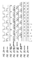
- Fig. 2 is a timing chart of the driving operation. In the following there will be explained the function in the normal drive with reference to Figs. 1 and 2.
- the device of the present invention receives the image information and the scanning line address information from the graphic controller 11, by the hand-shake method.
- the microcomputer in the drive control circuit 2 indicates to the graphic controller 11 that reception of data is possible, by shifting a signal HSYNC to the L-level.
- the graphic controller 11 transfer signals AH/DL and PD0 - PD7 (image information and scanning line address information) in synchronization with a clock signal CLK. Since the image information and the scanning line address information are transmitted through a same transmission channel, the AH/DL signal is used as the identification signal therefor. More specifically, the PD0-PD7 signal represents the scanning line address information or the image information respectively when said AH/DL signal is at the H- or L-level.
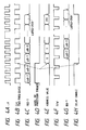
- Fig. 3 is a detailed block diagram of the drive control circuit 2 shown in Fig. 1, and Fig. 4 is a timing chart thereof.
- a microcomputer 31 serves to transfer the HSYNC signal to the graphic controller 11, receives the AH/DL signal, and controls the transmission of an AH/DL signal, a microcomputer trigger signal and a selection signal to a delay enable/trigger selection circuit 32.
- the microcomputer 31 can select either the AH/DL signal or the microcomputer trigger signal for effecting the delay enable triggering.
- the selected signal is supplied to the delay enable generator 33, and said signal and a clock signal obtained by 1/2 frequency division of the clock signal CLK from the graphic controller to generate a delay enable signal which is supplied to the delay circuit.
- the address counter 34 is reset to renew the data in the memory.
- the address counter 34 sends a memory stop signal to the delay enable generator 33, whereby the memory enable signal is shifted to the H-level to terminate the function of the delay circuit 1.
- the circuit 2 enables the rewriting of the delay circuit without the information transfer from the graphic controller 11.
- the selection signal supplied from the microcomputer 31 of the drive control circuit 2 to the delay enable/trigger selection circuit 32 is such that the AH/DL signal is used as the delay enable trigger signal.
- the microcomputer 31 maintains the HSYNC signal at the L-level, whereby the image information Ld (Ld0-7, Ld8-11, ..., Kd2552-2559) from the graphic controller 11 is transferred to the delay circuit 1 in synchronization with the clock signal CLK.
- the input information PD0-7 is supplied to the address detection circuit 3 for detecting the scanning address information (La0-7, La8-11, Ma0-7, ).
- the microcomputer 31 releases a drive start signal (line (b) in Fig. 1), thus latching the content of the shift register 4 in the line memory 5.
- the scanning line address information La is transferred from the address detection circuit to the decoder 7 and decoded therein to designate a line to be erased.
- Said period T1 corresponding to a horizontal scanning period 1H, or the time for rewriting a line.
- the drive is started by a drive start signal released from the microcomputer 31.
- the scanning line to be erased is designated by the decoder 7 (scanning line L in this example), and the pixels to be written in the scanning line (scanning line K in this example) are those set in the memory 8.
- Said lines L and K are simultaneously driven by the scanning signal generator 9.
- the driving voltage supplied to the scanning line L corresponds to an "erase phase” shown in Fig. 5, and that supplied to the line K corresponds to a "write phase” shown in Fig. 5.
- Fig. 5 there are shown a selection signal with voltage levels V1, V2 and V3, and a non-selection signal with voltage 0.
- the microcomputer 31 shifts the HSYNC signal to the L-level, for receiving next information PD0-7 from the graphic controller 11.
- the image information Md is transferred to the delay circuit 1 as explained above, and the preceding image information Ld is transferred to the shift register 4.
- the address detection circuit 3 detects the scanning line address information Ma. Then the microcomputer 31 releases the drive start signal, thus latching the image information Ld of the shift register 4 in the line memory 5.
- the scanning line address information Ma is transferred, in synchronization, to the decoder 7, and the designation of the scanning line L is set in the memory 8.
- a period T3 the pixels on the scanning line M are erased, and the pixels on the scanning line L are rewritten into black or white according to the image information Ld stored in the line memory 5.
- the microcomputer 31 shifts the HSYNC signal to the low level whereby the image information Nd is transferred to the delay circuit 1, and the image information Md is transferred to the shift register 4.
- the address detection circuit 3 detects the scanning line address information Na, and, in response to the drive start signal, the designation of the scanning line N is set in the decoder 7 while the designation of the scanning line M is set in the memory 8.
- the normal drive is thus conducted in succession according to the above-explained procedure.
- Fig. 10 is a flow chart showing the control sequence of the microcomputer 31 in the above-explained procedure. In the following there will be explained the procedure of an interruption drive, for modifying the drive wave form in the course of a drive, or for a partial rewriting.
- Fig. 6 is a timing chart of this drive. It is assumed that the microcomputer 31 detects, in a period T1, the necessity for temperature compensation or for a frame drive. More specifically, the microcomputer 31 is equipped with a counter for counting the number of scan designation, and constantly compares said number with the number of scan designations at which the temperature compensation or the frame drive has to be conducted. Thus the microcomputer 31 can recognize, at the reception of the information LD0-7, the necessity for temperature compensation or frame drive.
- the address detection circuit 3 detects the scanning line address information La, and the delay circuit 1 stores the image information Ld.
- the image information Kd is set in the line memory 5
- the scanning line address information La is set in the decoder 7
- the designation information of the scanning line K, designated in the period T1 is set in the memory 8.
- the writing is conducted in the scanning line K while the scanning line L is erased.
- the microcomputer 31 in order to prohibit the information transfer from the graphic controller 11, the microcomputer 31 maintains the HSYNC signal at the H-level. Then the delay enable/trigger selection circuit 32 of the drive control circuit 2 is switched from the AH/DL signal to the microcomputer trigger.
- the microcomputer 31 releases a delay enable trigger (microcomputer trigger) signal through a line (c) in Fig. 1.
- the image information from the delay circuit 1 is transferred to the shift register 4 without reception of information from the graphic controller 11.
- the address detection circuit 3 does not detect the scanning line address information, and the microcomputer 11 releases a non-selection signal (line (a) in Fig. 1) indicating the absence of selection of all the scanning lines.
- the designation of all the scanning lines is set in the decoder 7.
- the designation of the scanning line L is set in the memory 8.
- the image information Ld is latched in the line memory 5.
- the period T3 there is only conducted the writing of the scanning line L.
- the decoder 7 sets, in the period T2, the non-selection signal which disables all the chip selections of the decoder 7.
- the next information is received from the graphic controller 11 and stored in the delay circuit 1.
- the drive start signal is released to set the scanning line address information Ma in the decoder 7.
- the memory 8 there is set the designation of non-selection for all the scanning lines.
- a period T5 there is conducted preparation for re-starting the normal drive, and the scanning line M to be written after said re-start is erased, but the writing is prohibited.
- the normal drive with simultaneous erasure and writing is executed.
- Fig. 7 shows the driving wave form. In the following there will be explained the procedure when one-line partial re-writing is successively executed.
- Fig. 8 is a timing chart of said procedure. There is shown a case in which the scanning line L is successively designated.
- the normal drive In the period T1 there is executed the normal drive, in which the scanning line address information La1 designating the scanning line L is detected. Then in response to the drive start signal, the scanning line address information La1 is set in the decoder 7, and the scanning line K, detected in the preceding period, is designated by the memory 8. In the period T2, the address detection circuit 3 detects the scanning line address information La2 designating the scanning line L same as that detected in the period T1. In the normal drive, in response to the drive start signal, the scanning line address information La2 is set in the decoder 7, while the scanning line address information La1 is set in the memory 8, whereby the erasure and the writing are conducted simultaneously on a same line. Thus the normal drive cannot be conducted in this case.
- the microcomputer 31 stores the preceding address and compares it with the scanning line address information La2 detected in this period, and recognizes that a same scanning line has been designated twice in succession. In response to said recognition, the microcomputer 31 releases a non-selection signal, indicating the non-selection of all the scanning lines, instead of the scanning line address information La2, and said non-selection signal is set in the decoder 7 in response to the drive start signal.
- the scanning line address information La1 is set in the memory 8. In the period T3, there is only conducted the writing of the scanning line L, because of the function in the period T2.
- the microcomputer 31 prohibits the transfer of next information from the graphic controller 11, and supplies the scanning line address information La2, which is set in the decoder 7 in response to the drive start signal.
- the memory 8 stores the non-selection state for all the scanning lines.
- the period T4 there is only conducted the erasure of the scanning line L.
- the next information is transferred in this period, so that the image information Ld2 is entered into the shift register 4.
- the image information Ld2 is set in the line memory 5 while the scanning line address information Ma is set in the decoder 7, and the memory 8 releases information designating the scanning line L.
- the normal drive is restored in the period T5. However, if the address is again La in the period T4, there is conducted, in the period T5, an operation same as that in the period T3.
- Fig. 9 shows the driving wave form.
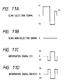
- Figs. 11A to 11D show the scanning selection signal, scanning non selection signal, white and black information signals employed in the present invention.
- the sequence of the scanning selection signal is same as shown in Fig. 5.
- the broken line portion of the information signal shown in Fig. 11C or 11D indicates a part of the preceding information signal.
- ferroelectric liquid crystal element disclosed, for example, in the U.S. Patent No. 4,639,089 of Okada et al., No. 4,709,994 of Kanbe et al., or No. 4,712,873 of Kanbe et al.
- a control device for prohibiting the input of the transferred information, a control circuit for enabling readout of the image information of at least a scanning line at an arbitrary time, and a circuit for selecting a non-selection state for all the addresses thereby interrupting the erasure of scanning line during the scanning period of a horizontal scanning line, whereby the scanning line to be selected next does not remain erased during the variation of the driving wave form or the frame drive. It is therefore rendered possible to prevent the presence of a black visible line, so that the correction of temperature characteristics, change of display mode or frame drive can be smoothly achieved in a display method in which at least two lines are simultaneously driven.
- a comparator for storing the preceding scanning line and comparing the same with the currently scanned line to achieve smooth drive in case one-line partial writing is required in succession, by switching from the erasure-writing simultaneous drive to the single-line drive.
Landscapes
- Engineering & Computer Science (AREA)
- Theoretical Computer Science (AREA)
- Physics & Mathematics (AREA)
- Crystallography & Structural Chemistry (AREA)
- Computer Hardware Design (AREA)
- General Physics & Mathematics (AREA)
- Chemical & Material Sciences (AREA)
- Liquid Crystal Display Device Control (AREA)
- Liquid Crystal (AREA)
- Selective Calling Equipment (AREA)
- Closed-Circuit Television Systems (AREA)
- Fittings On The Vehicle Exterior For Carrying Loads, And Devices For Holding Or Mounting Articles (AREA)
- Control Of Indicators Other Than Cathode Ray Tubes (AREA)
Claims (14)
- Dispositif d'excitation, comportant :
des électrodes en matrice composées de lignes de balayage (Ko, Lo, Mo, No) et de lignes d'informations ;
un circuit d'excitation de lignes d'informations ayant un circuit de conversion série-parallèle (4) et une première mémoire (5) pour stocker une information d'image (Kd, Ld, Md, Nd) provenant dudit circuit de conversion série-parallèle (4) ;
un circuit d'excitation de lignes de balayage ; et
des moyens de commande (2) destinés à commander ledit circuit d'excitation de lignes d'informations et ledit circuit d'excitation de lignes de balayage
ledit dispositif d'excitation étant caractérisé en ce que
ledit circuit d'excitation de lignes d'informations comporte en outre un circuit à retard (1) destiné à retarder le transfert d'une information d'image (Kd, Ld, Md, Nd) à écrire dans des pixels d'une ligne de balayage (Ko, Lo, Mo, No) audit circuit de conversion série-parallèle (4),
ledit circuit d'excitation de lignes de balayage comporte un circuit (7) de désignation de ligne de balayage destiné à générer une information de ligne de balayage qui désigne une ligne de balayage et une seconde mémoire (8) destinée à stocker l'information de ligne de balayage générée par ledit circuit (7) de désignation de ligne de balayage ;
lesdits moyens de commande (2) commandent ledit circuit d'excitation de lignes d'informations et ledit circuit de désignation de ligne de balayage afin que l'information d'image (Kd, Ld, Md, Nd) stockée dans ladite première mémoire (5), qui est utilisée pour un balayage de la Nième ligne, l'information de ligne de balayage provenant dudit circuit (7) de désignation de ligne de balayage qui est utilisée pour désigner une ligne de balayage (Ko, Lo, Mo, No) pour un balayage de la (N+1)ième ligne et l'information de ligne de balayage stockée dans ladite seconde mémoire (8) qui est utilisée pour désigner une ligne de balayage (Ko, Lo, Mo, No) pour un balayage de la Nième ligne soient délivrées en sortie en synchronisme, et que ladite information de ligne de balayage utilisée pour désigner la ligne de balayage (Ko, Lo, Mo, No) pour un balayage de la (N+1)ième ligne soit délivrée en sortie durant la délivrance en sortie de l'information de ligne de balayage pour le Nième balayage, et que des pixels sur la ligne de balayage désignée par l'information de ligne de balayage utilisée pour désigner la ligne de balayage (Ko, Lo, Mo, No) pour le balayage de la (N+1)ième ligne soient effacés et que les pixels sur la ligne de balayage (Ko, Lo, Mo, No) soient écrits conformément à ladite information de ligne de balayage utilisée pour désigner la ligne de balayage (Ko, Lo, Mo, No) pour un balayage de la Nième ligne et ladite information d'image (Kd, Ld, Md, Nd) stockée dans ladite première mémoire (5) utilisée pour le balayage de la Nième ligne. - Dispositif d'excitation selon la revendication 1, caractérisé en ce que lesdits moyens de commande (2) comportent en outre des moyens (32 ; 33) destinés à commander ledit circuit d'excitation de lignes d'informations et ledit circuit d'excitation de lignes de balayage, lorsque le nombre de désignations de lignes de balayage (Ko, Lo, Mo, No) atteint une valeur prédéterminée, afin d'empêcher le transfert d'une information d'image (Kd, Ld, Md, Nd) audit circuit (1) de retard, et durant l'application des signaux de tension d'écriture aux pixels de la ligne de balayage (Ko, Lo, Mo, No) désignée conformément à l'information provenant de ladite seconde mémoire (8), afin d'appliquer un signal de non-sélection aux autres lignes de balayage (Ko, Lo, Mo, No).
- Dispositif d'excitation selon la revendication 2, caractérisé en ce que lesdits moyens de commande comprennent un compteur (34) destiné à compter un nombre de désignations des lignes de balayage (Ko, Lo, Mo, No).
- Dispositif d'excitation selon la revendication 1, caractérisé en ce que lesdits moyens de commande (2) comportent en outre des moyens (32, 33) destinés à commander ledit circuit d'excitation de lignes d'informations et ledit circuit d'excitation des lignes de balayage, dans le cas où la même ligne de balayage (Ko, Lo, Mo, No) est désignée de façon successive, afin d'empêcher le transfert de l'information d'image (Kd, Ld, Md, Nd) audit circuit (1) de retard et, durant l'application des signaux de tension d'écriture aux pixels de la ligne de balayage (Ko, Lo, Mo, No) désignée conformément à l'information provenant de ladite seconde mémoire (8), d'appliquer un signal de non-sélection aux autres lignes de balayage (Ko, Lo, Mo, No).
- Dispositif d'excitation selon la revendication 4, caractérisé en ce que lesdits moyens de commande (2) comprennent des moyens (31) destinés à comparer le contenu de l'information entrée (Ka, La, Ma, Na) d'adresse de ligne de balayage.
- Dispositif d'excitation selon l'une quelconque des revendications précédentes 1 à 5, caractérisé en ce qu'un cristal liquide ferroélectrique est disposé entre le ligne de balayage (Ko, Lo, Mo, No) et la ligne d'informations.
- Système d'affichage, comportant :
un panneau d'affichage (10) comportant des électrodes en matrice composées de lignes de balayage (Ko, Lo, Mo, No) et de lignes d'informations ;
des premiers moyens (11) destinés à transférer une information d'adresse de ligne de balayage (Ka, La, Ma, Na) et une information d'image (Kd, Ld, Md, Nd) correspondant à l'écriture dans des pixels d'une ligne de balayage (Ko, Lo, Mo, No) ;
ledit système d'affichage étant caractérisé en ce qu'il comporte en outre
des deuxièmes moyens (1) destinés à retarder le transfert de l'information d'image (Kd, Ld, Md, Nd) reçue desdits premiers moyens, puis à bloquer l'information d'image (Kd, Ld, Md, Nd) d'une ligne de balayage (Ko, Lo, Mo, No) ; et
des troisièmes moyens (7) destinés à désigner une ligne de balayage d'effacement (K, L, M, N) en décodant l'information d'adresse reçue de ligne de balayage (Ka, La, Ma, Na) en tant que premier signal et en délivrant en sortie le premier signal à un circuit (9) de génération de ligne de balayage, pour simultanément stocker ledit premier signal dans une mémoire (8) et désigner une ligne de balayage d'image en délivrant en sortie un second signal précédemment stocké dans ladite mémoire (8) audit circuit (9) de génération de ligne de balayage. - Système d'affichage selon la revendication 7, caractérisé en ce que ledit panneau d'affichage (10) possède un effet de mémoire.
- Système d'affichage selon la revendication 7, caractérisé en ce que ledit panneau d'affichage (10) comporte un cristal liquide ferroélectrique.
- Système d'affichage selon la revendication 7, caractérisé en ce que lesdits troisièmes moyens (7) comprennent en outre des moyens destinés à effectuer une excitation sélective pour effacer uniformément, dans la période de ladite synchronisation, les pixels de la ligne de balayage désignés conformément à ladite information d'adresse (Ka, La, Ma, Na) de ligne de balayage.
- Système d'affichage selon la revendication 7, caractérisé en ce qu'il comporte en outre des quatrièmes moyens (2) destinés à invalider un signal désignant la ligne de balayage d'effacement lorsque le nombre de lignes de balayage d'image désignées atteint une valeur prédéterminée.
- Système d'affichage selon la revendication 7, caractérisé en ce que lesdits troisièmes moyens (7) destinés à désigner une ligne de balayage d'effacement en décodant l'information d'adresse reçue (Ka, La, Ma, Na) de ligne de balayage en tant que premier signal et en délivrant en sortie le premier signal à un circuit (9) de génération de ligne de balayage, pour simultanément stocker ledit premier signal dans une mémoire (8) et délivrer en sortie un second signal désignant une ligne de balayage d'image précédemment stocké dans ladite mémoire (8) audit circuit (9) de génération de signal de balayage durant la sortie dudit premier signal, et comportant en outre des quatrièmes moyens (2) pour invalider un signal désignant la ligne de balayage d'effacement lorsque le nombre de lignes de balayage d'image désignées atteint une valeur prédéterminée.
- Système d'affichage selon la revendication 7, caractérisé en ce que lesdits troisièmes moyens (7) destinés à désigner une ligne de balayage d'effacement en décodant l'information reçue (Ka, La, Ma, Na) d'adresse de ligne de balayage en tant que premier signal et en délivrant en sortie le premier signal à un circuit (9) de génération de ligne de balayage, pour simultanément stocker ledit premier signal dans une mémoire (8) et désigner une ligne de balayage d'image en délivrant en sortie un second signal précédemment stocké dans ladite mémoire (8) audit circuit (9) de génération de ligne de balayage, et comportant en outre des quatrièmes moyens (2) destinés à commander lesdits deuxièmes (1) et troisièmes (7) moyens de manière que la ligne de balayage désignée par un signal désignant la ligne de balayage d'effacement soit excitée de façon non sélective lorsque la désignation de la même ligne de balayage d'image apparaît de façon successive.
- Système d'affichage selon la revendication 7, caractérisé en ce que lesdits troisièmes moyens (7) destinés à désigner (a) une ligne de balayage d'effacement en décodant l'information reçue (Ka, La, Ma, Na) d'adresse de ligne de balayage en tant que premier signal et en délivrant en sortie le premier signal à un circuit (9) de génération de ligne de balayage, pour simultanément stocker ledit premier signal dans une mémoire (8) et délivrer en sortie un second signal désignant une ligne de balayage d'image stockée précédemment dans ladite mémoire (8) audit circuit (9) de génération de signal de balayage durant la sortie dudit premier signal ; et comportant en outre des quatrièmes moyens (2) pour invalider un signal désignant la ligne de balayage d'effacement lorsque le nombre de lignes de balayage d'image désignées atteint une valeur prédéterminée.
Applications Claiming Priority (2)
| Application Number | Priority Date | Filing Date | Title |
|---|---|---|---|
| JP1225380A JP2584871B2 (ja) | 1989-08-31 | 1989-08-31 | 表示装置 |
| JP225380/89 | 1989-08-31 |
Publications (2)
| Publication Number | Publication Date |
|---|---|
| EP0414960A1 EP0414960A1 (fr) | 1991-03-06 |
| EP0414960B1 true EP0414960B1 (fr) | 1994-08-10 |
Family
ID=16828448
Family Applications (1)
| Application Number | Title | Priority Date | Filing Date |
|---|---|---|---|
| EP89121720A Expired - Lifetime EP0414960B1 (fr) | 1989-08-31 | 1989-11-24 | Dispositif d'entraînement et système d'affichage |
Country Status (8)
| Country | Link |
|---|---|
| US (1) | US5353041A (fr) |
| EP (1) | EP0414960B1 (fr) |
| JP (1) | JP2584871B2 (fr) |
| KR (1) | KR940002293B1 (fr) |
| AT (1) | ATE109917T1 (fr) |
| AU (1) | AU617017B2 (fr) |
| DE (1) | DE68917469T2 (fr) |
| ES (1) | ES2057074T3 (fr) |
Families Citing this family (24)
| Publication number | Priority date | Publication date | Assignee | Title |
|---|---|---|---|---|
| US5757352A (en) * | 1990-06-18 | 1998-05-26 | Canon Kabushiki Kaisha | Image information control apparatus and display device |
| JPH05210085A (ja) * | 1992-01-30 | 1993-08-20 | Canon Inc | 表示制御装置 |
| JPH06274133A (ja) * | 1993-03-24 | 1994-09-30 | Sharp Corp | 表示装置の駆動回路及び表示装置 |
| JP3346843B2 (ja) * | 1993-06-30 | 2002-11-18 | 株式会社東芝 | 液晶表示装置 |
| JP3307750B2 (ja) * | 1993-12-28 | 2002-07-24 | キヤノン株式会社 | 表示制御装置 |
| JPH07199891A (ja) * | 1993-12-28 | 1995-08-04 | Canon Inc | 表示制御装置 |
| JP3266402B2 (ja) * | 1993-12-28 | 2002-03-18 | キヤノン株式会社 | 表示装置 |
| KR100295712B1 (ko) * | 1994-03-11 | 2001-11-14 | 미다라이 후지오 | 컴퓨터디스플레이시스템컨트롤러 |
| JPH08101669A (ja) * | 1994-09-30 | 1996-04-16 | Semiconductor Energy Lab Co Ltd | 表示装置駆動回路 |
| JPH08278486A (ja) * | 1995-04-05 | 1996-10-22 | Canon Inc | 表示制御装置及び方法及び表示装置 |
| US5933128A (en) * | 1995-05-17 | 1999-08-03 | Canon Kabushiki Kaisha | Chiral smectic liquid crystal apparatus and driving method therefor |
| KR100337865B1 (ko) * | 1995-09-05 | 2002-12-16 | 삼성에스디아이 주식회사 | 액정 표시 소자의 구동방법 |
| JP3492083B2 (ja) * | 1996-05-17 | 2004-02-03 | キヤノン株式会社 | 画像表示装置 |
| JPH1069251A (ja) | 1996-08-29 | 1998-03-10 | Canon Inc | 表示装置、表示システム及び画像処理装置 |
| US6538675B2 (en) | 1998-04-17 | 2003-03-25 | Canon Kabushiki Kaisha | Display control apparatus and display control system for switching control of two position indication marks |
| US7148909B2 (en) * | 1998-05-27 | 2006-12-12 | Canon Kabushiki Kaisha | Image display system capable of displaying and scaling images on plurality of image sources and display control method therefor |
| US6473088B1 (en) | 1998-06-16 | 2002-10-29 | Canon Kabushiki Kaisha | System for displaying multiple images and display method therefor |
| JP4508330B2 (ja) | 1999-01-25 | 2010-07-21 | キヤノン株式会社 | 表示装置 |
| JP3469116B2 (ja) * | 1999-01-28 | 2003-11-25 | シャープ株式会社 | 表示用駆動装置およびそれを用いた液晶モジュール |
| CN1161738C (zh) * | 1999-03-15 | 2004-08-11 | 精工爱普生株式会社 | 液晶显示装置及其驱动方法 |
| JP3712046B2 (ja) * | 2000-05-30 | 2005-11-02 | 富士通株式会社 | 液晶表示装置 |
| US20040179754A1 (en) * | 2002-11-26 | 2004-09-16 | Nossi Taheri | Reclosable multi-compartment bag with an integrated pouch |
| TWI421836B (zh) * | 2010-05-12 | 2014-01-01 | Au Optronics Corp | 顯示裝置及其顯示方法以及電流驅動元件的驅動電路 |
| CN115428064B (zh) * | 2020-04-24 | 2024-09-20 | 京瓷株式会社 | 点矩阵型显示装置以及计时装置 |
Citations (1)
| Publication number | Priority date | Publication date | Assignee | Title |
|---|---|---|---|---|
| EP0308927A1 (fr) * | 1987-09-22 | 1989-03-29 | Fraunhofer-Gesellschaft Zur Förderung Der Angewandten Forschung E.V. | Pièces formées, en particulier pour véhicules |
Family Cites Families (27)
| Publication number | Priority date | Publication date | Assignee | Title |
|---|---|---|---|---|
| US3716658A (en) * | 1967-06-13 | 1973-02-13 | M Rackman | Liquid-crystal television display system |
| US4655561A (en) * | 1983-04-19 | 1987-04-07 | Canon Kabushiki Kaisha | Method of driving optical modulation device using ferroelectric liquid crystal |
| US5093737A (en) * | 1984-02-17 | 1992-03-03 | Canon Kabushiki Kaisha | Method for driving a ferroelectric optical modulation device therefor to apply an erasing voltage in the first step |
| JPS60172029A (ja) * | 1984-02-17 | 1985-09-05 | Canon Inc | 液晶装置 |
| US4638309A (en) * | 1983-09-08 | 1987-01-20 | Texas Instruments Incorporated | Spatial light modulator drive system |
| GB2146473B (en) * | 1983-09-10 | 1987-03-11 | Standard Telephones Cables Ltd | Addressing liquid crystal displays |
| US4715688A (en) * | 1984-07-04 | 1987-12-29 | Seiko Instruments Inc. | Ferroelectric liquid crystal display device having an A.C. holding voltage |
| FR2558606B1 (fr) * | 1984-01-23 | 1993-11-05 | Canon Kk | Procede de commande d'un dispositif de modulation optique et dispositif de modulation optique pour sa mise en oeuvre |
| US4701026A (en) * | 1984-06-11 | 1987-10-20 | Seiko Epson Kabushiki Kaisha | Method and circuits for driving a liquid crystal display device |
| JPS6118929A (ja) * | 1984-07-05 | 1986-01-27 | Seiko Instr & Electronics Ltd | 強誘電性液晶電気光学装置 |
| US4709995A (en) * | 1984-08-18 | 1987-12-01 | Canon Kabushiki Kaisha | Ferroelectric display panel and driving method therefor to achieve gray scale |
| JPS6152630A (ja) * | 1984-08-22 | 1986-03-15 | Hitachi Ltd | 液晶素子の駆動方法 |
| JPS6167833A (ja) * | 1984-09-11 | 1986-04-08 | Citizen Watch Co Ltd | 液晶表示装置 |
| DE3508321A1 (de) * | 1985-03-06 | 1986-09-11 | CREATEC Gesellschaft für Elektrotechnik mbH, 1000 Berlin | Programmierbare schaltung zur steuerung einer fluessigkristallanzeige |
| GB2185614B (en) * | 1985-12-25 | 1990-04-18 | Canon Kk | Optical modulation device |
| US4770502A (en) * | 1986-01-10 | 1988-09-13 | Hitachi, Ltd. | Ferroelectric liquid crystal matrix driving apparatus and method |
| EP0529701B1 (fr) * | 1986-08-18 | 1998-11-11 | Canon Kabushiki Kaisha | Dispositif d'affichage |
| JPS6363093A (ja) * | 1986-09-03 | 1988-03-19 | キヤノン株式会社 | 表示装置 |
| DE3784809T2 (de) * | 1986-08-18 | 1993-07-08 | Canon Kk | Verfahren und vorrichtung zur ansteuerung einer optischen modulationsanordnung. |
| GB8622714D0 (en) * | 1986-09-20 | 1986-10-29 | Emi Plc Thorn | Display device |
| JPS63138316A (ja) * | 1986-11-29 | 1988-06-10 | Toppan Printing Co Ltd | 液晶表示方法 |
| US4901066A (en) * | 1986-12-16 | 1990-02-13 | Matsushita Electric Industrial Co., Ltd. | Method of driving an optical modulation device |
| JP2579933B2 (ja) * | 1987-03-31 | 1997-02-12 | キヤノン株式会社 | 表示制御装置 |
| EP0291252A3 (fr) * | 1987-05-12 | 1989-08-02 | Seiko Epson Corporation | Procédé et dispositif d'affichage vidéo |
| GB8720856D0 (en) * | 1987-09-04 | 1987-10-14 | Emi Plc Thorn | Matrix addressing |
| JPH06105390B2 (ja) * | 1987-09-25 | 1994-12-21 | キヤノン株式会社 | 液晶装置の信号転送方式 |
| JP2632974B2 (ja) * | 1988-10-28 | 1997-07-23 | キヤノン株式会社 | 駆動装置及び液晶装置 |
-
1989
- 1989-08-31 JP JP1225380A patent/JP2584871B2/ja not_active Expired - Fee Related
- 1989-11-23 AU AU45496/89A patent/AU617017B2/en not_active Ceased
- 1989-11-24 DE DE68917469T patent/DE68917469T2/de not_active Expired - Fee Related
- 1989-11-24 ES ES89121720T patent/ES2057074T3/es not_active Expired - Lifetime
- 1989-11-24 AT AT89121720T patent/ATE109917T1/de not_active IP Right Cessation
- 1989-11-24 EP EP89121720A patent/EP0414960B1/fr not_active Expired - Lifetime
- 1989-12-30 KR KR1019890020387A patent/KR940002293B1/ko not_active Expired - Fee Related
-
1991
- 1991-11-04 US US07/787,739 patent/US5353041A/en not_active Expired - Fee Related
Patent Citations (1)
| Publication number | Priority date | Publication date | Assignee | Title |
|---|---|---|---|---|
| EP0308927A1 (fr) * | 1987-09-22 | 1989-03-29 | Fraunhofer-Gesellschaft Zur Förderung Der Angewandten Forschung E.V. | Pièces formées, en particulier pour véhicules |
Also Published As
| Publication number | Publication date |
|---|---|
| US5353041A (en) | 1994-10-04 |
| AU4549689A (en) | 1991-03-07 |
| ATE109917T1 (de) | 1994-08-15 |
| KR910005219A (ko) | 1991-03-30 |
| ES2057074T3 (es) | 1994-10-16 |
| DE68917469T2 (de) | 1994-12-15 |
| EP0414960A1 (fr) | 1991-03-06 |
| AU617017B2 (en) | 1991-11-14 |
| KR940002293B1 (ko) | 1994-03-21 |
| JP2584871B2 (ja) | 1997-02-26 |
| JPH0387815A (ja) | 1991-04-12 |
| DE68917469D1 (de) | 1994-09-15 |
Similar Documents
| Publication | Publication Date | Title |
|---|---|---|
| EP0414960B1 (fr) | Dispositif d'entraînement et système d'affichage | |
| JP3556150B2 (ja) | 液晶表示方法および液晶表示装置 | |
| US5321419A (en) | Display apparatus having both refresh-scan and partial-scan | |
| US4662718A (en) | Expansion system for a liquid crystal display | |
| US7176947B2 (en) | Device for driving a display apparatus | |
| US6947034B2 (en) | Impulse driving method and apparatus for LCD | |
| EP0424958B1 (fr) | Dispositif d'affichage à cristaux liquides avec mise hors-circuit controlée | |
| EP0368117B1 (fr) | Système d'affichage | |
| US4985698A (en) | Display panel driving apparatus | |
| US6847339B2 (en) | Method and device for driving plasma display panel | |
| JP2003280599A (ja) | 表示装置及びその駆動方法 | |
| US5929833A (en) | Matrix liquid crystal display having temperature-dependent element drive timing and method of driving the same | |
| US7499010B2 (en) | Display, driver device for same, and display method for same | |
| CA2038687C (fr) | Methode et dispositif d'excitation pour afficheur matriciel actif a cristaux liquides | |
| US5289175A (en) | Method of and apparatus for driving ferroelectric liquid crystal display device | |
| US6597335B2 (en) | Liquid crystal display device and method for driving the same | |
| CN113345358A (zh) | 适用于动态更新率的应用的显示驱动电路 | |
| KR940005238B1 (ko) | 표시장치 및 구동회로 | |
| KR100357945B1 (ko) | 액정 표시 소자 구동 회로 | |
| JP3016369B2 (ja) | 映像表示装置 | |
| JP2578490B2 (ja) | 表示装置の駆動法 | |
| US6359600B1 (en) | Matrix display device for displaying a lesser number of video lines on a greater number of display lines | |
| JPH02709B2 (fr) | ||
| JP2827990B2 (ja) | 液晶表示装置 | |
| JPH0573001A (ja) | 液晶表示装置の駆動方法 |
Legal Events
| Date | Code | Title | Description |
|---|---|---|---|
| PUAI | Public reference made under article 153(3) epc to a published international application that has entered the european phase |
Free format text: ORIGINAL CODE: 0009012 |
|
| 17P | Request for examination filed |
Effective date: 19901221 |
|
| AK | Designated contracting states |
Kind code of ref document: A1 Designated state(s): AT BE CH DE ES FR GB GR IT LI LU NL SE |
|
| 17Q | First examination report despatched |
Effective date: 19930211 |
|
| GRAA | (expected) grant |
Free format text: ORIGINAL CODE: 0009210 |
|
| AK | Designated contracting states |
Kind code of ref document: B1 Designated state(s): AT BE CH DE ES FR GB GR IT LI LU NL SE |
|
| PG25 | Lapsed in a contracting state [announced via postgrant information from national office to epo] |
Ref country code: GR Free format text: LAPSE BECAUSE OF FAILURE TO SUBMIT A TRANSLATION OF THE DESCRIPTION OR TO PAY THE FEE WITHIN THE PRESCRIBED TIME-LIMIT Effective date: 19940810 Ref country code: AT Effective date: 19940810 |
|
| REF | Corresponds to: |
Ref document number: 109917 Country of ref document: AT Date of ref document: 19940815 Kind code of ref document: T |
|
| REF | Corresponds to: |
Ref document number: 68917469 Country of ref document: DE Date of ref document: 19940915 |
|
| REG | Reference to a national code |
Ref country code: ES Ref legal event code: FG2A Ref document number: 2057074 Country of ref document: ES Kind code of ref document: T3 |
|
| ITF | It: translation for a ep patent filed | ||
| ET | Fr: translation filed | ||
| ITTA | It: last paid annual fee | ||
| PG25 | Lapsed in a contracting state [announced via postgrant information from national office to epo] |
Ref country code: LU Free format text: LAPSE BECAUSE OF NON-PAYMENT OF DUE FEES Effective date: 19941130 |
|
| EAL | Se: european patent in force in sweden |
Ref document number: 89121720.0 |
|
| PLBE | No opposition filed within time limit |
Free format text: ORIGINAL CODE: 0009261 |
|
| STAA | Information on the status of an ep patent application or granted ep patent |
Free format text: STATUS: NO OPPOSITION FILED WITHIN TIME LIMIT |
|
| 26N | No opposition filed | ||
| REG | Reference to a national code |
Ref country code: GB Ref legal event code: IF02 |
|
| PGFP | Annual fee paid to national office [announced via postgrant information from national office to epo] |
Ref country code: SE Payment date: 20021106 Year of fee payment: 14 |
|
| PGFP | Annual fee paid to national office [announced via postgrant information from national office to epo] |
Ref country code: FR Payment date: 20021108 Year of fee payment: 14 |
|
| PGFP | Annual fee paid to national office [announced via postgrant information from national office to epo] |
Ref country code: GB Payment date: 20021120 Year of fee payment: 14 |
|
| PGFP | Annual fee paid to national office [announced via postgrant information from national office to epo] |
Ref country code: ES Payment date: 20021127 Year of fee payment: 14 |
|
| PGFP | Annual fee paid to national office [announced via postgrant information from national office to epo] |
Ref country code: DE Payment date: 20021128 Year of fee payment: 14 |
|
| PGFP | Annual fee paid to national office [announced via postgrant information from national office to epo] |
Ref country code: NL Payment date: 20021129 Year of fee payment: 14 Ref country code: CH Payment date: 20021129 Year of fee payment: 14 |
|
| PGFP | Annual fee paid to national office [announced via postgrant information from national office to epo] |
Ref country code: BE Payment date: 20030117 Year of fee payment: 14 |
|
| PG25 | Lapsed in a contracting state [announced via postgrant information from national office to epo] |
Ref country code: GB Free format text: LAPSE BECAUSE OF NON-PAYMENT OF DUE FEES Effective date: 20031124 |
|
| PG25 | Lapsed in a contracting state [announced via postgrant information from national office to epo] |
Ref country code: SE Free format text: LAPSE BECAUSE OF NON-PAYMENT OF DUE FEES Effective date: 20031125 Ref country code: ES Free format text: LAPSE BECAUSE OF NON-PAYMENT OF DUE FEES Effective date: 20031125 |
|
| PG25 | Lapsed in a contracting state [announced via postgrant information from national office to epo] |
Ref country code: LI Free format text: LAPSE BECAUSE OF NON-PAYMENT OF DUE FEES Effective date: 20031130 Ref country code: CH Free format text: LAPSE BECAUSE OF NON-PAYMENT OF DUE FEES Effective date: 20031130 Ref country code: BE Free format text: LAPSE BECAUSE OF NON-PAYMENT OF DUE FEES Effective date: 20031130 |
|
| BERE | Be: lapsed |
Owner name: *CANON K.K. Effective date: 20031130 |
|
| PG25 | Lapsed in a contracting state [announced via postgrant information from national office to epo] |
Ref country code: NL Free format text: LAPSE BECAUSE OF NON-PAYMENT OF DUE FEES Effective date: 20040601 |
|
| PG25 | Lapsed in a contracting state [announced via postgrant information from national office to epo] |
Ref country code: DE Free format text: LAPSE BECAUSE OF NON-PAYMENT OF DUE FEES Effective date: 20040602 |
|
| EUG | Se: european patent has lapsed | ||
| GBPC | Gb: european patent ceased through non-payment of renewal fee |
Effective date: 20031124 |
|
| REG | Reference to a national code |
Ref country code: CH Ref legal event code: PL |
|
| PG25 | Lapsed in a contracting state [announced via postgrant information from national office to epo] |
Ref country code: FR Free format text: LAPSE BECAUSE OF NON-PAYMENT OF DUE FEES Effective date: 20040730 |
|
| NLV4 | Nl: lapsed or anulled due to non-payment of the annual fee |
Effective date: 20040601 |
|
| REG | Reference to a national code |
Ref country code: FR Ref legal event code: ST |
|
| REG | Reference to a national code |
Ref country code: ES Ref legal event code: FD2A Effective date: 20031125 |
|
| PG25 | Lapsed in a contracting state [announced via postgrant information from national office to epo] |
Ref country code: IT Free format text: LAPSE BECAUSE OF NON-PAYMENT OF DUE FEES;WARNING: LAPSES OF ITALIAN PATENTS WITH EFFECTIVE DATE BEFORE 2007 MAY HAVE OCCURRED AT ANY TIME BEFORE 2007. THE CORRECT EFFECTIVE DATE MAY BE DIFFERENT FROM THE ONE RECORDED. Effective date: 20051124 |