EP0415319A2 - Verfahren und Gerät zur Prüfung von Leiterplatten mit gesteuerter Rückspeisungsbelastung - Google Patents
Verfahren und Gerät zur Prüfung von Leiterplatten mit gesteuerter Rückspeisungsbelastung Download PDFInfo
- Publication number
- EP0415319A2 EP0415319A2 EP90116386A EP90116386A EP0415319A2 EP 0415319 A2 EP0415319 A2 EP 0415319A2 EP 90116386 A EP90116386 A EP 90116386A EP 90116386 A EP90116386 A EP 90116386A EP 0415319 A2 EP0415319 A2 EP 0415319A2
- Authority
- EP
- European Patent Office
- Prior art keywords
- methods
- test
- testing
- circuit
- nodes
- Prior art date
- Legal status (The legal status is an assumption and is not a legal conclusion. Google has not performed a legal analysis and makes no representation as to the accuracy of the status listed.)
- Granted
Links
Images


Classifications
-
- G—PHYSICS
- G01—MEASURING; TESTING
- G01R—MEASURING ELECTRIC VARIABLES; MEASURING MAGNETIC VARIABLES
- G01R31/00—Arrangements for testing electric properties; Arrangements for locating electric faults; Arrangements for electrical testing characterised by what is being tested not provided for elsewhere
- G01R31/28—Testing of electronic circuits, e.g. by signal tracer
- G01R31/2801—Testing of printed circuits, backplanes, motherboards, hybrid circuits or carriers for multichip packages [MCP]
- G01R31/2806—Apparatus therefor, e.g. test stations, drivers, analysers, conveyors
-
- G—PHYSICS
- G01—MEASURING; TESTING
- G01R—MEASURING ELECTRIC VARIABLES; MEASURING MAGNETIC VARIABLES
- G01R31/00—Arrangements for testing electric properties; Arrangements for locating electric faults; Arrangements for electrical testing characterised by what is being tested not provided for elsewhere
- G01R31/28—Testing of electronic circuits, e.g. by signal tracer
- G01R31/317—Testing of digital circuits
- G01R31/3181—Functional testing
- G01R31/319—Tester hardware, i.e. output processing circuits
- G01R31/31903—Tester hardware, i.e. output processing circuits tester configuration
- G01R31/31915—In-circuit Testers
-
- G—PHYSICS
- G01—MEASURING; TESTING
- G01R—MEASURING ELECTRIC VARIABLES; MEASURING MAGNETIC VARIABLES
- G01R31/00—Arrangements for testing electric properties; Arrangements for locating electric faults; Arrangements for electrical testing characterised by what is being tested not provided for elsewhere
- G01R31/28—Testing of electronic circuits, e.g. by signal tracer
- G01R31/30—Marginal testing, e.g. by varying supply voltage
- G01R31/3004—Current or voltage test
Definitions
- This invention is related to those disclosed in the commonly-assigned United States Patent Nos. 4,555,783 (issued November 26, 1985 to Swanson and entitled METHOD OF COMPUTERIZED IN-CIRCUIT TESTING OF ELECTRICAL COMPONENTS AND THE LIKE WITH AUTOMATIC SPURIOUS SIGNAL SUPPRESSION) and 4,459,693 (issued July 10, 1984 to Prang, et al. and entitled METHOD OF AND APPARATUS FOR THE AUTOMATIC DIAGNOSIS OF THE FAILURE OF ELECTRICAL DEVICES CONNECTED TO COMMON BUS NODES AND THE LIKE), which are both incorporated herein by reference.
- the present invention pertains to automatic testing of electronic circuits, and more particularly to improved test techniques for digital devices.
- ATE's Programmable, computer-controlled instruments and systems for testing printed circuit boards and electronic components thereon are called “automatic test equipment” or “ATE's.”
- ATE's include functional testers and in-circuit testers.
- a functional tester tests overall functionality of a board-under-test, "BUT,” i.e., how the electronic components and circuits of the BUT function collectively.
- Functional testing of a portion of a circuit board is called “cluster testing.”
- functional and cluster testers test so-called functions-under- test ("FUT's").
- in-circuit testers test individual devices-under-test ("DUT's").
- DUT's devices-under-test
- ATE's are used to detect manufacturing defects, such as short circuits (e.g., a solder bridge between the etched, conductive tracks on the BUT), faulty assembly of electronic components on the BUT, or defective devices themselves.
- in-circuit testers can detect defects in digital logic devices such as integrated circuits ("IC's"). To accomplish such testing, the IC's are exercised and checked against their truth tables. More specifically, the tester applies pre-selected drive.signals to inputs of the DUT's, monitors or detects the responses to the drive signals on the outputs of the DUT's, and compares the detected responses with expected or predicted responses for those devices.
- IC's integrated circuits
- Nodes are the electrical connections between the leads of electronic components of the BUT, e.g., the etched, conductive tracks on the pc board that extend between various output leads and input leads of electronic components on the BUT.
- a test fixture aptly named a "bed-of-nails” fixture.
- the “nails” in this fixture typically are a plurality (e.g., hundreds) of probes, each typically being a spring-loaded pin, that electrically contact the nodes on the BUT during testing.
- Some of the nails supply the drive signals to the BUT, and others receive the response signals from the BUT.
- the nails are inserted in sockets so located on the fixture as to maintain the nails in registration with the selected circuit nodes with which they are to make electrical connection. Connections between the fixture and the tester are made by wiring the other end of the sockets to electrical connectors in the tester.
- the physical interface between the fixture and the tester is called the "receiver.”
- a conventional tester has sets of digital drivers that it uses to drive the IC inputs to desired voltage states, and a set of digital sensors to check the logic levels at the IC outputs.
- These drivers and sensors typically form driver/sensor testing pairs ("D/S"), in which the output of a driver is tied to the input of an associated sensor.
- D/S driver/sensor testing pairs
- BUT nodes contacted by the D/S pairs each can be either driven by a current supplied by the driver or tracked, i.e., have its current sensed by the sensor of the D/S pair.
- Drivers and sensors preferably are separately controllable by the tester.
- the driver When a D/S pair is used to place an IC input in a desired voltage state, the driver is enabled (connected) and a suitable voltage is applied to the IC input. Then, the sensor of another D/S pair is enabled to sense the response to that drive signal at an IC output.
- the following test patterns could be followed: a) the drivers of the D/S pairs, which are associated with the test nails which, in turn, are connected to inputs N0, N1, are enabled, b) a voltage selected to place these inputs N0, N1 in the HIGH state is applied to those drivers, c) the sensor of each of the D/S pair, which is associated with the tester nail which, in turn, is connected to output N3, is enabled, and d) the sensor is controlled to check for a LOW output from the NAND gate.
- Such complex digital tests routinely are conducted with presently manufactured testers, typically at speeds faster than the testers' central processing units (“CPU's”) can control in real time. Therefore, the CPU's typically load series of test patterns into memory banks. Then, to start the tests, the CPU's enable high-speed controllers, which transfer the test patterns to the drivers and store the responses detected by the sensors in the memory banks. After the test procedures are completed, the CPU's transfer the results of the tests from the memory banks to main memory for later analysis.
- CPU's central processing units
- test isolation An additional complication arising in in-circuit testing is test isolation.
- Driven nodes (i.e., circuit interconnections) on the pc board typically are connected not only to the inputs of the DUT's but also to inputs and/or outputs of other electronic components. Consequently, many electronic components on the pc board, in addition to DUT's, typically are energized simultaneously by the drive signals.
- the tester must be able to electrically isolate each DUT from the other electronic components to which they are electrically connected.
- Analog devices are isolated, e.g., by conventional techniques collectively referred to as "guarding.”
- Digital devices typically are isolated by a process known as "backdriving.
- Backdriving can be understood with continued reference to the example given above.
- the test requires that input N1 be held HIGH, but further suppose that input N1 is connected to a node which the output of another IC, called an "upstream” or “predecessor” device, ordinarily would be driving to a LOW value.
- the tester can handle this conflict in logic states by momentarily forcing N1 to the desired HIGH state regardless of the state to which it is being held by the upstream IC.
- This technique of momentarily overriding an IC output is called “backdriving.”
- backdriving is the process of forcing the output of an up-stream digital device to a logic level different from that to which the digital device is "trying" to drive it.
- backdriving is carried out by applying to a node (called a “controlled node”) a backdriving current that exceeds the drive capacity of the device to whose output the node is connected, and thus is sufficient in amplitude to change the voltage state of that node.
- a controlled node By controlling the state of the controlled node, the DUT's input node or nodes (called “protected nodes”) are placed in desired logic states.
- the controlled nodes are those which are connected immediately between the outputs of up-stream electronic components and the inputs of the DUT's. When that is the case, the controlled nodes are also protected nodes.
- the controlled nodes are other nodes of the BUT, e.g., nodes connected to the inputs to the upstream electronic components.
- the backdriving currents cause the inputs of those upstream electronic components to assume values that result in outputs at the desired voltage levels, and, these voltage levels are applied to the protected nodes leading to the inputs of the DUT's.
- the backdriving signals applied to upstream electronic components propagate through the circuit and eventually yield the desired state on the protected nodes.
- bused devices i.e., several digital devices all having outputs connected to a common bus.
- the tester must check each device individually to see if each one can control the logic state of the bus.
- any defective device could force the bus to an erroneous state at which, for example, the bus would remain despite an ouput from another of the devices which normally would place the bus in a different state. In other words, the bus is "stuck" in the erroneous state.
- the problem is to identify which, if any, of the electronic components is the defective one.
- the isolation protocol consists of a plurality of isolation methods, one for each DUT. Each isolation method is a procedure for placing one or more outputs of an IC that is up-stream from the DUT being isolated into a specified logic state by driving one or more inputs of that IC (or of a device up-stream from that IC) into selected logic states or a sequence of selected logic states.
- each such available method entails the identification of a set of nodes to be controlled in order to protect the specified protected node, and the specification of backdriving currents required to effect that control.
- an inhibit method prevents a glitch from propagating into the output so as to keep the output constant, and, normally, to drive the output into the weaker state.
- TTL transistor-transistor logic
- an inhibit method attempts to drive the output into the HIGH state which is typically the weaker state.
- a disable method forces an output into an OFF state.
- An H-force method forces the output into a HIGH state
- an L-force method forces the output into a LOW state.
- isolation methods The selection of which of the available types of isolation methods to use is made by analyzing the BUT's topology and the characteristics of the electronic components contained thereon. Of course, where a BUT has a plurality. of protected nodes, a plurality of isolation methods may be selected for implementation during testing, each isolation method causing one or more of the protected nodes to assume the desired logic state therefor.
- the tester inhibits the NAND gate in the feedback loop, thereby eliminating the glitch-sensitive feedback signal and permitting the glitch-free testing of the flip-flop.
- a tester typically disables all tri-state electronic components (i.e., digital devices having outputs that can be HIGH, LOW, or a high-impedance state) by placing them in their high-impedence state, and inhibits all other electronic components (except for the DUT's) by forcing their inputs to a state that effectively inhibits their operation.)
- the protocol for testing the common bus example, given above, to determine which device is defective and is keeping the bus stuck in one state entails disabling all of the devices (e.g. by placing them in their high impedence state) and measuring the bus current, then enabling each device separately, one at a time, applying logic inputs to the enabled devices that tend to drive the bus to that one state, and measuring the resulting bus currents. If the bus current changes significantly, the enabled device is not faulty, but if the current remains substantially the same as when the device was disabled, then that device is regarded as faulty.
- Backdriving strategies for the common bus scenario are discussed in the above-referenced U.S. Pat. No. 4,459,693.
- the isolation needed for accurate and reliable in-circuit testing is achieved by using a combination of methods of applying backdrive currents to the BUT, which methods collectively constitute the isolation protocol for the BUT.
- backdrive currents can present their own problems in testing pc boards.
- backdrive currents generally are of greater amplitude than, and are directed in the opposite direction with respect to, the currents normally flowing in the controlled nodes. Consequently, the up-stream devices with respect to those nodes experience reverse currents that flow into the up-stream devices through their output power leads. The effects of these currents on the up-stream devices is called "backdrive stress.” While these currents often do not present a problem, the rise in temperature attributable to these currents can cause damage to the up-stream devices, i.e., under certain conditions the up-stream devices can experience excessive backdrive stress.
- fixed cool-down intervals of pre-determined length commonly are introduced between the pulses or bursts of the driving signals in order to reduce adverse temperature effects of excessive backdrive strees, e.g., by permitting the devices to cool to room temperature.
- Another known technique is to use variable (instead of fixed) cool-down intervals.
- An example of this technique is disclosed by U.S. Patent No. 4,588,945 issued to Groves.
- records containing topological descriptions of the BUT, and pre-generated generic test patterns for the DUT's are provided.
- a topological analyzer sorts through these records, selects patterns which are suitable for testing each DUT, and supplies these patterns to a damage analyzer.
- the damage analyzer receives the selected test patterns and calculates the time the test will require, and, using safeguard parameters stored with the topological records, calculates the length of the inter-burst times necessary to avoid damage to up-stream components that would otherwise occur.
- the safeguard parameters are not used in selecting the test patterns, but, rather, they are used only after the test patterns are selected, in the calculation of the cool-down periods. Subsequently, a test controller applies the test patterns to DUT's through a driver module, inserting the calculated inter-burst delays when and where appropriate.
- circuit board testing is recognized as a significant part of quality assurance programs. Improvements in the reliability, safety, efficacity, efficiency and economics of circuit board test and diagnostic techniques represent marked advances in the manufacture of electronic products of high quality. Recent trends toward higher-powered logic families and larger IC's with many parallel outputs (e.g., gate arrays) have made more evident the problems of excessive backdrive stress resulting from such testing.
- the invention resides in improved automatic testing equipment and systems for performing in-circuit, functional or cluster tests which take backdrive stress into account in selecting appropriate isolation methods-- e.g., inhibits, disables, H-forces, and L-forces-- during the generation of the test protocols.
- the generation of each test protocol includes an analysis of the circuit board and its components, and of the available methods to isolate the device- or function-under-test from the rest of the circuit board.
- Tha analysis includes a calculation of "total stress current" flowing in each upstream component to determine if these currents are below a safety threshold (e.g., 1 ampere), and the selection of a combination of methods from those available which among other considerations) will produce total stress currents below this threshold.
- a safety threshold e.g., 1 ampere
- Stress current is the incremental increase in current flowing into an output power lead of a component due to backdriving.
- the stress currents resulting from backdriving the power leads HIGH, each symbolized as “I osh ,” all flow through the device to, e.g., the V cc lead.
- the stress currents resulting from backdriving the power leads LOW, each symbolized as “I osh ,” all flow through the device to, e.g., ground.
- the “total stress current” is the greater of the resulting currents flowing through the V cc and ground leads.
- Bond wires are the small conductors within the IC packages that connect the semiconductor chips to the components' leads.
- the V cc bond wire connects the chip to the V cc lead
- the ground bond wire connects the chip to the ground lead.
- Backdrive stress generally will not damage the up-stream devices as long as the total stress currents flowing through the V cc and/or ground bond wires have amplitudes and durations below safe limits.
- the backdrive stress resulting from the chosen methods of isolation is excessive, i.e., the total stress current flowing through the V cc and ground bond wires are above a safety threshold for one or more devices on the BUT, damage to those devices can result from the test. Therefore, as mentioned above, the calculation of total stress currents that would result from implementing the available methods of isolation of a BUT are calculated and the resulting value is used in selecting the isolation methods to be used in running the test.
- a suitable value for the safety threshold has been found to be 1 ampere, although an even higher threshold can be used for some devices.
- the system then can proceede to use the selected methods in running the test. On the other hand, if all combinations of the methods produce excessive backdrive stress, the test equipment alerts the operator of this condition.
- GLOBAL MAXTIME a maximum length of time under which the test can run safely is calculated before running the test.
- GLOBAL MAXTIME is an approximation of the minimal length of time before which the calculated total stress currents would overheat the V cc and ground bond wires of the up-stream IC's.
- the methods of isolation are chosen to assure that the stress currents are below a selected maximum amplitude as described in the preceding paragraphs, and, then, the GLOBAL MAXTIME is calculated to assure that the effects of the calculated total stress currents over time will not damage the up-stream devices were those selected methods implemented.
- test can not be run in a period of time under the GLOBAL MAXTIME, it would be unsafe to run the test.
- the test can be run in a period of time under the GLOBAL MAXTIME, the test as generated by the system can safely proceede. For example, if the GLOBAL MAXTIME is approximately 7 milliseconds, the test typically can be successfully run.
- the invention provides an automated backdrive stress management and control system for in-circuit, functional, and cluster testing of printed circuit boards.
- Each test run by the improved ATE in accordance herewith is characterized by an inter-burst time period equal to the time it takes to load the next test to be performed. This time period typically is of sufficient length to allow the temperature to decline to approximately ambient temperature. It should be emphasized, however, that the invention does not use the inter-burst cool-down interval, as in the prior art, as the control variable to eliminate the adverse temperature effects of excessive backdrive stress. Rather, the invention uses calculations for the stress currents, themselves, in the design of the test to eliminated the potential for excessive backdrive stress during the running of the test.
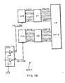
- an integrated circuit DUT1 is to be in-circuit tested.
- Electronic devices U9 and U17 are up-stream devices with respect to DUT1, i.e., devices having one or more outputs electrically connected to one or more inputs of DUT1.
- U6 is up-stream of U9
- U44 is up-stream of U17
- inverter U67 is upstream of both DUT1 and U7
- U33 is up-stream of U6, U9 and U67.
- the outputs of U17 and U9 can be disabled or U9 and U17 can be inhibited.
- the analysis of different methods of disabling the outputs of U17 and U9 will be presented.
- a similar analysis of methods of achieving the inhibiting of U9 and U17 can be derived by those skilled in the art.
- the circuit analysis to achieve the desired disabling is as follows-- First, an analysis of circuit topology yields an identification of nodes available for backdriving. For example, one method of achieving the disablement is to use nodes SEL_AI and SEL2_AI (i.e., the enable inputs of U17 and U9) to disable (e.g., tri-state) the outputs of U17 and U9. It is possible that U17 cannot be disabled in this way, however, because SEL2_AI is unavailable.
- a technique for reducing the currents required to backdrive U17 involves controlling the nodes connecting U44 to U17 in order to generate better (i.e., more easily backdriven) output signals from U17. For example, U44's outputs could be backdriven to force U17's outputs to the weaker "HIGH" state, which would protect U17 by avoiding the need for the application of the higher backdriving currents to the U17 outputs.
- SEL_ND, SEL_AI and ENCLK_DA could be driven to disable the respective outputs of U6, U9 and U67. While each of the resulting stress currents in SEL_ND, SEL_AI and ENCLK_DA individually might be at a safe level, the total stress current experienced by U33 could be excessive. If this were the case, it could be avoided by driving the TP3 line LOW to protect U33. on the other hand, if TP3 were not available for this purpose, U33's outputs could be driven into a weak (HIGH) state to avoid the difficulty; however, if the signals present on the U33 inputs were too strong, then a testability problem would be present.
- SEL_ND, SEL_AI and ENCLK_DA could be driven to disable the respective outputs of U6, U9 and U67. While each of the resulting stress currents in SEL_ND, SEL_AI and ENCLK_DA individually might be at a safe level, the total stress current experienced by U33 could be excessive. If this were
- DUT2 is the device-under-test.
- DUT2 and devices U6, U7, and U70 are, e.g., IC's designated SN74LS240 and made by Texas Instruments, Dallas, Texas, USA.
- Devices U6, U7 drive DUT2 over respective lines ODATO through ODAT7 and ODAT8 through ODAT15.
- Device U13 drives device U7 over lines DAT0 through DAT7
- device U14 drives device U6 over lines DAT8 through DAT15.
- Devices U13, U14 are both, e.g., SN74ALS374 IC's, made also by Texas Instruments.
- device U70 drives U13 over line SEL-LOB, and drives U14 over line SEL-HIB.
- lines 0DAT0 through 0DAT15 are nodes that are to be protected, i.e., placed or maintained in pre-selected states, e.g., LOGIC LOW values, for testing, regardless of the states to which these lines are being driven by up-stream devices U6, U7. Because of this, the lines 0DAT0 - 0DAT15 are regarded as "target nodes,” or simply "targets.”
- a direct approach would be to apply drive signals directly to the targets 0DAT0 - 0DAT15 to force these lines into the desired states. For the sake of this example, suppose that this direct approach can not be used because of glitch sensitivity in lines 0DAT0 - 0DAT15.
- values for I osh and I osl are determined as follows: If an output from the device is disabled, both I osh and I osl equal to zero for the output; if held HIGH by both the tester drive signals energizing the device for the test and the selected methods of isolation, I osh equals zero for the output; and if held LOW by both the tester drive signals and the selected methods of isolation, I osl equals zero for the output.
- the values for these currents must be calculated based on the manufacturers' specifications for the device and the amplitude of backdriving currents supplied by the tester. This calculation is well within the skill in the art.
- I osl is equal to -0.225 ampere for each output DAT0 through DAT15. Since there are eight of these outputs for each device U13, U14 that are all being driven LOW, the value for I osl is multiplied by eight to yield a total stress current, i.e., a total incremental power lead current, for either device U13 or U14 of -1.8 amps.
- the total stress current for a device is the greater of the sum of the I osh values for the device and the sum of the I osl values for the device.
- the nodes DAT0-DAT15 are added to the list of nodes to be protected, i.e., are considered additional target nodes, and the aforementioned method of isolation is deemed inappropriate unless further action is taken.
- input lines SEL_LOB and SEL_HIB of devices U13, U14 can be driven so as to force each output DAT0-DAT7 and DAT8-DAT15 to either a high-impedance or HIGH state.
- a method of accomplishing this entails driving both the nodes SEL_LOB and SEL_HIB to HIGH states. This turns off the respective outputs DATO-DAT7 and DAT8-DAT15 of U13 and U14, so I osl is equal to zero for each lead of U13 AND U14, and the stress currents in U13 and U14 are reduced to zero.
- MAXTIME (T/k) [1/(I b )2]
- T is the maximum safe temperature to which the bond wires can be heated, which typically is 250°C
- k is an empirically derived constant having a value of 36,000 for bond wire materials and lengths used in conventional IC packages
- I b is the stress current, equal to the sum of I osh values for nodes being backdriven to a LOGIC HIGH state and to the sum of I osl values for nodes being backdriven to a LOGIC LOW state.
- a typical value for MAXTIME for the given example is 30 milliseconds. This is regarded as a sufficient length of time to conduct this in-circuit test.
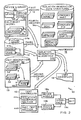
- FIGURE 2 shows an improved automatic test equipment or system 10 for generating an optimal test isolation protocol for a BUT, such as either of those shown in FIGURES 1A or 1B, and for using that protocol for testing the BUT.
- the system 10 has a first memory 12, a second memory 13, a third memory 14, a processor 16, a fourth memory 16a, a user interface 18, a test controller 19, a driver module 19a and a sensor module 19b.
- An interface unit 19c electrically connects the tester modules 19a, 19b to the nodes of the BUT.
- the interface unit 19c preferably includes a bed-of-nails fixture and a receiver, neither of which being separately shown in FIGURE 2.
- the memories 12, 13, 14 and 16a can be implemented separately or as sections of a main memory.
- the first memory 12 stores a device library 20.
- the device library includes a device model 22, an in-circuit model 24, and a device leads table 25.
- the device model 22 is a table listing operational parameters and specifications for a plurality of commercially-available electronic devices (e.g, output currents, maximum reverse currents, and values of resistors, capacitors, ...) as specified and published by manufacturers.
- the in-circuit model 24 contains a plurality of sections 24a, 24b,...24n, which contain information and data concerning the methods-- e.g., inhibits, disables, H-forces, and L-forces-- by which various digital devices described in the device model library can be isolated during testing.
- commercially available IC are cross-referenced with a set of methods available (at least in theory) for isolating that IC. It should be understood that not all methods listed in the in-circuit model 24 will be available for testing the BUT however. Some methods might be unavailable for particular IC's, or particular applications of particular IC's, e.g., because of wiring conflicts.
- the device leads table 25 identifies the leads of the electrical devices lists in the device model 22.
- each of the in-circuit model sections 24a-24n and the device leads table 25 constitute separately accessible records stored.in locations of the first memory 12. A better understanding of the contents of the first memory 12 will be obtained from the discussion of FIGURE 3 and FIGURES 4A-4F, below.
- the second memory 13 stores BUT descriptions 30, i.e., descriptions of circuit topology of the BUT.
- the BUT descriptions includes a parts table 32 which describes the components (e.g., gates, multiplexors%) contained in the BUT, a nodes table 34 which lists the nodes on the BUT, and a leads table 36 which lists the BUT component leads, and, for each, identifies the nodes or nodes to which it is electrically connected.
- Each of the parts, nodes, and leads tables 32, 34, 36 contains a plurality of separately accessible records (designated by a suffix a,b,..n added to the respective reference numeral) stored in locations of the second memory 13.
- the third memory 14 stores a fixture library 37, i.e., data concerning the interface unit 19c.
- the fixture library 37 contains a nodes table 37a and a tester pins table 37b.
- the nodes table 37a cross-references each node of the BUT to the tester pin or pins (i.e., nail or nails), if any, which it contacts during testing.
- the tester pins table 37b cross-references each tester pin (i.e., nail) to the node which it contacts during testing.
- the processor 16 receives selected sections 24 and selected entries from the device leads table 25 from the first memory 12, selected entries from the parts, nodes and leads tables 32, 34, 36 from the second memory 13, and selected entries from the nodes table 37a and tester pins table 37b from the third memory 37, all of which are associated with the BUT, and processes this data in accordance with a test isolation generation algorithm 100 (which is described in considerable detail in conjunction with FIGURES 3 and 4A-4F) to yield data that is supplied to the user interface 18 and/or to yield a test protocol that is supplied to the test controller 19.
- the fourth memory 16a coupled to the processor 16, stores data structures (described below) generated by the processor 16.
- the user interface 18 receives the resulting data from the processor 16. It either converts the data from machine readable form to human readable form, or stores it for later use.
- the user interface 18 preferably can display on a cathode ray tube ("CRT"), or print out in tangible form, a stress report and/or warnings concerning the level of backdrive stress or test run-time.
- CTR cathode ray tube
- the processor 16 also provides information concerning the optimal test protocol to the test controller 19.
- the test controller 19 is shown in FIGURE 2 as including an isolation waveform section 44a responsible for controlling the test patterns (i.e., waveforms) to be supplied to the BUT in accordance with the isolation protocol computed by the processor 16. These patterns are characterized by safe levels of stress currents for isolation of devices on the BUT.
- the test controller 19 also has a part test section 44b responsible for processing the response signals from the DUT's.
- the outputs from sections 44a, 44b are supplied to the tester driver module 19a, which provides drive signals to the BUT.
- a tester sensor module 19b receives response signals resulting from the drive signals from the BUT and also receives expected response signals from the test controller 19, and provides, to the test controller 19, signals indicating whether the expected response signals, in fact, were received.
- the tester modules 19a, 19b can be implemented using the driver/sensor amplifier circuit disclosed in U.S. Patent No. 4,594,558 entitled "HIGH-SWITCHING SPEED D.C. AMPLIFIER WITH INPUT-OFFSET CURRENT COMPENSATION,” and issued June 10, 1986.
- FIGURE 3 shows an isolation generation algorithm 100, represented in flow chart form, for use by the processor 16 in generating an optimal isolation protocol (sometimes also called an "isolation procedure,” “isolation strategy” or “isolation methodology”).
- the algorithm 100 differs from the prior art in that it adds backdrive stress to the considerations that determine the preferred isolation protocol.
- the algorithm 100 identifies a particular set of test isolation methods-- e.g., inhibits, disables, H-forces, and L-forces-- which, when used in running the test, maintain stress currents at acceptable levels, and thereby eliminate excessive backdrive stress. For any reason, if the algorithm 100 is unable to identify test methods which avoid excessive stress currents, and which can be performed within necessary time constraints for running the test, the algorithm 100 appropriately cautions the user accordingly.
- the algorithm 100 is entered at block 101 with pre-selected lists of DUT's and of nodes to be protected.
- the list of nodes is used as a reference into the nodes table 32 of memory 13 (FIGURE 2) for fetching information from which algorithm IOO forms a table of TARGETS, i.e., an associated list of data structures or records stored in memory 13 that identify and describe nodes to be protected.
- TARGETS i.e., an associated list of data structures or records stored in memory 13 that identify and describe nodes to be protected.
- lines 0DAT0 - 0DAT15 are targets, and for each of these a TARGET record is created.
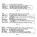
- FIGURE 4A A preferred format for a TARGET record is shown in FIGURE 4A as including an "int id” field which provides an identification number for this TARGET, a "NODE *pnode” field which identifies the node to be protected (i.e., the target), an "int why” field which identifies the reason for protecting this node (as determined by the algorithm 100 from an analysis of the DUT Description Library 30), a "SET *pgoals” field which identifies the set of GOALS (described below) required to protect this target.
- a table called GOALS is created by fetching appropriate data corresponding to the TARGETS from the leads table 36 of second memory 13 (FIGURE 2).
- GOALS are data structures which each describe a node that is to be controlled by the test controller 19 (FIGURE 1) in order to protect the TARGETS.
- a separate GOAL record is created for each such node.
- the lines DATO - DAT15 are goals to be controlled in order to protect the targets 0DAT0 - 0DAT15.
- FIGURE 4B A preferred format for a GOAL record is shown in FIGURE 4B as including an "int Id” field which provides an identification number for this GOAL, a “PART *ppart” field which identifies the component or components of the BUT to which this goal is electrically connected, “SET *leads” field which identifies a set of component leads to which this GOAL is electrically connected, an "int why” field which identifies the objective for this GOAL (as determined by the algorythm 100 from an analysis of the DUT Description Library, e.g., to protect a specified node for specified reasons), an "int priority” field which specifies the importance of meeting this GOAL (described below), an "int chosen” field which later has a value of NEGATIVE ONE if rejected (i.e., the ,goal is not controlled during testing), and a value greater than ZERO if the "Method id” field of METHOD (described below) indicates that
- a table called METHODS is created by fetching the methods from the in-circuit model table 24 of the first memory 12 (FIGURE 2) which can isolate the devices of the BUT which drive the goals (i.e., the nodes described in the GOAL records).
- the METHODS table contains data structures that describe methods-- e.g., inhibits, disables, H-forces, and L-forces-- for isolating DUT's on the BUT, and thereby controlling the goals.
- Separate METHOD records are created for each method identified as available in the in-circuit model 24 for protecting any one or more of the goals.
- the METHODS records contain data pertaining to methods of isolation that are available for commercially available IC's and each method can protect one or more nodes on the BUT. From the available methods, the algorithm 100 selects the optimal one for each TARGET, and analyzes the affects of implementing that selected method on each other protected and controlled node, as will be explained shortly.
- FIGURE 4C A preferred format for a METHOD record is shown in FIGURE 4C as including an "int Id” field which provides an identification number for this METHOD, a "SECTION *psec” field which describes the method, e.g., nodes that are protected using this method, nodes that are controlled using this method, amplitude of backdriving currents (as determined by the algorithm 100 by analyzing the in-circuit model 24 (FIGURE 2), with due consideration of the BUT topology described in the BUT description library 30 and the contents of the fixture library 37), an "int why" field of entries each corresponding to a GOAL identifying this method, each entry gives the most important (i.e., highest) reason for each GOAL to need this METHOD, an "int chosen” field of entries each corresponding to a GOAL identifying this method, each entry later having a value of NEGATIVE ONE if this method of isolation is rejected by algorithm 100, POSITIVE ONE if this method is accepted for implementation in
- STRESSED PART table which contains information stored in the PARTS table 34 of memory 13 and the device model 22 of first memory 12.
- PARTS table 34 of memory 13 contains information stored in the PARTS table 34 of memory 13 and the device model 22 of first memory 12.
- Each of these data structures later will store the results of various calculations (with respect to the particular electronic components of the BUT) that are performed during the remaining steps of the algorithm 100.
- FIGURE 4D A preferred format for a STRESSED PART record is shown in FIGURE 4D as including a "PART *ppart” field which identifies an electronic component of the BUT whose backdrive stress is being tracked, a "SET *nodes” field which gives the node ids for those nodes at which the tester is currently backdriving this electronic component, a "Iosh_sum” field which will store a calculated total stress current flowing through the V cc bond wire of this part, an “Iosl_sum” field which will store a calculated total stress current flowing through the ground bond wire of this part, a “Max_I” field which contains the maximum allowable total stress current for this electronic component (i.e., typically 1 ampere), a "Max time” field which will store a calculated maximum test time allowed at the values of total stress currents given in the Iosh_sum and Iosl_sum fields for the methods selected for implementation, and a "set *stressed leads” field which provides a set of
- a STRESSED LEAD table is created, and data fetched from the leads table 25 of memory 13. It lists leads of the parts on the DUT, and, in association with each listed lead that is backdriven and with each method of isolation involving backdriving one or more of the listed leads, the table also provides values for I osh and I osl .
- FIGURE 4E A preferred format for a STRESSED LEAD record is shown in FIGURE 4E as including a "int ID” field which provides an identification number for this STRESSED LEAD; a “lead ID” field which identifies the component lead that is being tracked; a “PART *ppart” field which identifies the electronic component of the BUT to which this lead is attached; an "Iosh” field which specifies the calculated stress current on this lead resulting from backdriving HIGH, i.e., I osh ; and an "Iosl” field which specifies the calculated stress current on this lead resulting from backdriving LOW, i.e., I osl .
- a NODAL CONFLICT table is formed so that it is available for insertion of data later generated in algorithm 100.
- a preferred format for a NODAL CONFLICT record is shown in FIGURE 4F as including a "NODE *pnode” field which specifies a node whose conflicting logic states are being tracked, an "Int conflicts” field which specifies the number of hold conflicts on this node, a "SET *HI_methods” field which identifies the methods which hold this node HIGH, and a "SET *LOW_methods” field which identifies the methods which hold this node LOW.
- a REPORT-RESULTS table is formed is available for insertion of the results of the algorithm 100.
- a preferred format for the REPORT-RESULTS table is shown in FIGURE 4G as including a "set *stress_part” field which specifies whether the chosen method or methods generate excessive stress for each stressed part identified in the STRESSED PART data structure, and a "GLOBAL MAXTIME” field which specifies the GLOBAL MAXTIME calculated for the test when the chosen methods are implemented.
- the TARGET, GOAL, METHOD, STRESSED PART, STRESSED LEAD, NODAL CONFLICT and REPORT-RESULTS tables for the BUT are all stored in fourth memory 16a (FIGURE 2), and the algorithm 100 next processes this information in a series of nested loops.
- the algorithm 100 tests whether all GOALS records have been processed. If the answer is NO, then the next step is described in block 114 as a sort-- GOALS records are sorted, i.e., ranked, in decreasing order of priority based on the contents of the "int priority" field of the GOAL record.
- the algorithm does this since the various reasons for protecting the TARGET vary in importance, and it may not be possible to protect all nodes that should be protected. In determining which ones will be protected, therefore, the algorithm ranks the GOALS in the order of their importance, and processes them in the order of their ranking.
- the GOALS are ranked in descending order of priority, for example, as follows:
- one or more additional GOALS can be added during subsequent steps of the algorithm 100, as indicated by item (3) in the ranking and as explained below. If GOALS are added, the GOAL sorting step to be repeated.
- the algorithm 100 at decision block 116 checks whether all GOALS records have been sorted, or have been fully processed, i.e., finished. If the answer is NO, (i.e., either further sorting or processing is required) one of the GOAL's that have been assigned the highest priority which has not as yet been fully processed is selected as the current GOAL in step 118. (Goals which have not as y,at been processed are called "unresolved.")
- decision block 120 all methods which achieve to the current GOAL are consecutively tested (i.e. tested one after another) to determine if any of them have not as yet been examined (as described below).
- the METHODS are referenced by the "SET *methods" field of the GOAL data structure for the current GOAL. If this test results in a YES, then the algorithm 100 flows next to block 122 where the next unexamined METHOD is fetched from memory 40 (FlGURE 2).
- the fetched METHOD for the current GOAL is examined, i.e., the resulting total stress currents on all stressed parts of the BUT are calculated, as described above, based on conditions which would prevail if the method corresponding to that METHOD record were chosen for implementation.
- This calculation uses the values of I osh and I osl which are associated with the fetched method and stored in the "Iosh” and “Iosl” fields of the corresponding STRESSED LEAD record.
- the calculated HIGH and LOW total stress currents carried by all leads of each DUT part are stored in the respective "Iosh_Sum” and "Iosl_Sum” fields of the corresponding STRESSED PART record.
- the number of nodal conflicts is calculated for the fetched METHOD in block 124.
- a conflict arises when the logic state of the current GOAL required to implement the method of the fetched METHOD record is not compatible with the logic state to which the current GOAL must be driven by the drive signals in order to run the test or in order to implement chosen methods of isolation that have already been selected. Computed holding node conflicts are stored in the NODAL CONFLICT table.
- the algorithm 100 loops back to the decision block 120, as indicated by line L-1, until all METHODS for the current GOAL have been examined. If there are no more METHODS left unexamined, the test of decision block 120 produces a NO, and the process of generating the optimal isolation methods next proceeds to block 126.
- decision block 126 the now-examined METHODS for the current GOAL are tested to assure that not all produce excessive backdrive stress. For this, the contents of each Iosh_sum and Iosl_sum field stored in the STRESSED PART data structure for each stressed part is compared with the upper safe threshold of total stress current, "I MAX ,” that is stored in the MAX_I field of the STRESS PART data structure for that part.
- I MAX typically is equal to 1 ampere, although the test operator can determine empirically or sometimes from manufacturers' specifications that an even higher value can be used, in which case this higher value would be placed in the MAX_I field and used in this test). If not all methods produce excessive stress, as indicated by the backdriving currents being below the I MAX threshold, the test of block 126 produces a NO, and next the algorithm 100 goes to block 128.
- the algorithm selects from among the methods which do not produce excessive total stress current, the method yielding the fewest nodal conflicts.
- the METHOD record corresponding to this selected method is called the Chosen METHOD and is so identified by having its Method Id stored in the "int chosen" field of the GOAL data structure for the current GOAL. Also, a POSITIVE ONE is entered in the "int chosen" field of the METHOD data structure at a location corresponding to the GOAL id for the current GOAL that is contained in the "SET *goals" field.
- the "int chosen" fields of all other METHODS that are listed in the NODAL CONFLICT data structure will be set appropriately with a NEGATIVE ONE, ZERO or POSITIVE ONE to indicate for each, for the current GOAL, that the METHOD was either rejected, neither accepted nor rejected (since further processing in algorithm 100 is necessary), or accepted, respectively.
- the algorithm 100 goes to block 134.
- the METHOD which results in the lowest total stress current is selected as the chosen METHOD. Since this chosen METHOD, if implemented, would result in total stress current above the safe threshold for the stressed part, the nodes that are connected to the part's outputs are added to the list of TARGET nodes in block 136. In other words, the TARGETS will now include not only nodes which are to be protected since they are inputs to the DUT's, but also those nodes which must be protected because of unintended effects of the chosen METHOD for the current GOAL.
- the algorithm 100 also sets a flag to indicate that the Goals are no longer sorted, i.e., "NOT SORTED" equals true. To handle this, the algorithm 100 returns over line L-2 to the "GOALS Finished or not Sorted?" decision block 116, and since the GOALS are no longer sorted, this decision generates a YES. This returns the program over line L-3 to the "GOALS finished?" decision block 112 and the ensuing block 114 where GOAL re-sorting occurs.
- the program returns over line L-2 to decision block 116, where, if not all GOALS have been resolved, i.e., have corresponding chosen METHODS, the test produces a NO and the program flows again to block 118 to select the next-highest-priority, unresolved GOAL for processing as a new Current GOAL, as described above. If the GOALS must be re-sorted, as indicated by the flag set in block 136, the test of block 116 again produces a NO, and the algorithm 100 goes again to block 114, and sorting and processing provede as described above.
- GLOBAL MAXTIME is the shortest MAXTIME for any of the chosen methods. As noted above, MAXTIME is the maximum length of time the chosen method can be safely run for a part without overheating the part, more specifically, without overheating the V cc and ground bondwires in the part.
- a loop is entered in which the total stress current resulting from the implementation of all the chosen methods is calculated for each stressed part, and the GLOBAL MAXTIME is determined.
- This loop begins with decision block 142, in which the algorithm 100 chooses a next stressed part as the "current stressed part," i.e., the subject of the calculations for the next pass through the loop.
- the total stress current that would flow in the current stressed part if all the chosen methods were implemented is calculated, as described above, and is stored in the appropriate Iosh-sum or Iosl-sum fields of the STRESSED PART record for the current stressed part.
- the MAXTIME for implementing the chosen methods with respect to the current stressed part is calculated, as described above, and stored in the MAX-TIME field of the STRESSED PART record for the current stressed part.
- the algorithm 100 determines whether the total stress currents calculated in block 144 produce excessive stress on the current stress part by comparing them with the upper threshold for stressed currents stored in the MAX-I field, as described above. lf the computed stressed currents for the current stressed part are excessive, i.e., exceed the MAX-I threshold, the test of block 146 produces a YES, and the algorithm 100 proceedses to block 148 wherein this result is noted by setting the entry for the current stressed part in the set *stress-part field of the REPORT-RESULTS data structure in memory 16a.
- the algorithm 100 proceedses to block 150.
- the MAXTlME for the current stressed part is compared with all previously-computed MAXTlMES for other stressed parts in block 150. lf the computed MAXTIME for the current stressed part is the shortest, the GLOBAL MAXTIME field of the REPORT-RESULTS data structure is set in bloc): 152 to equal this value. Afterwards, or if it is not the shortest value, the algorithm 100 returns over line L-5 to block 142. There, the algorithm 100 fetches the next stressed part for processing as the current stressed part, as described above.
- test of block 142 indicates this and the algorithm 100 ends.
- the processor 16 of FIGURE 2 can issue a report of the results of the algorithm 100 over the user interface 18.
- the report can include the contents of the REPORT-RESULTS record, i.e., the identification of which, if any, of the stressed parts would have excessive total stress currents if the chosen methods were inplemented, and the value of the GLOBAL MAXTIME, i.e., the maximum safe time the test can be permitted to run. Based on this report, the test operator then can intervene, as required, to assure the test is safely run.
- any BUT parts were identified as being subject to excessive stress if the test were inplemented with the chosen methods, the operator can introduce new methods of isolation, e.g., inhibits, disables, H-forces, and/or L-forces, for particular nodes (i.e., change the contents of the in-circuit model 24 (FIGURE 2), and re-run the algorithm 100.
- This is a viable option in many cases since the determination of which methods are available for isolation, and, therefore, included in the in-circuit model 24, is made with a tendency to exclude any methods which have a non-insignificant chance of damaging the BUT.
- the Chosen METHODS are fed to the test controller 19 (FlGURE 2) and the test can proceed using the isolation protocol thus computed.
Landscapes
- Engineering & Computer Science (AREA)
- General Engineering & Computer Science (AREA)
- Physics & Mathematics (AREA)
- General Physics & Mathematics (AREA)
- Computer Hardware Design (AREA)
- Microelectronics & Electronic Packaging (AREA)
- Tests Of Electronic Circuits (AREA)
- Testing Of Individual Semiconductor Devices (AREA)
Applications Claiming Priority (2)
| Application Number | Priority Date | Filing Date | Title |
|---|---|---|---|
| US399853 | 1982-07-19 | ||
| US07/399,853 US5127009A (en) | 1989-08-29 | 1989-08-29 | Method and apparatus for circuit board testing with controlled backdrive stress |
Publications (3)
| Publication Number | Publication Date |
|---|---|
| EP0415319A2 true EP0415319A2 (de) | 1991-03-06 |
| EP0415319A3 EP0415319A3 (en) | 1991-09-25 |
| EP0415319B1 EP0415319B1 (de) | 1997-05-21 |
Family
ID=23581238
Family Applications (1)
| Application Number | Title | Priority Date | Filing Date |
|---|---|---|---|
| EP90116386A Expired - Lifetime EP0415319B1 (de) | 1989-08-29 | 1990-08-27 | Verfahren und Gerät zur Prüfung von Leiterplatten mit gesteuerter Rückspeisungsbelastung |
Country Status (4)
| Country | Link |
|---|---|
| US (1) | US5127009A (de) |
| EP (1) | EP0415319B1 (de) |
| JP (1) | JP3281367B2 (de) |
| DE (1) | DE69030755T2 (de) |
Cited By (2)
| Publication number | Priority date | Publication date | Assignee | Title |
|---|---|---|---|---|
| US6114848A (en) * | 1999-01-14 | 2000-09-05 | Genrad, Inc. | Direct-measurement provision of safe backdrive levels |
| CN108920371A (zh) * | 2018-07-05 | 2018-11-30 | 郑州云海信息技术有限公司 | 一种存储管理系统的qat功能自动化测试方法及系统 |
Families Citing this family (15)
| Publication number | Priority date | Publication date | Assignee | Title |
|---|---|---|---|---|
| US5252914A (en) * | 1990-08-06 | 1993-10-12 | Ericsson Ge Mobile Communications Inc. | Method of constructing and testing a circuit board designed for early diagnostics |
| US5404584A (en) * | 1990-08-06 | 1995-04-04 | Ericsson Ge Mobile Communications Inc. | Printed circuit board having modularized circuit functions designed for early diagnostics |
| EP0881572B1 (de) * | 1997-05-28 | 2001-10-10 | Agilent Technologies, Inc. (a Delaware corporation) | Permanente Fehlerüberwachung in komplexen Systemen |
| US6243853B1 (en) * | 1998-10-02 | 2001-06-05 | Agilent Technologies, Inc. | Development of automated digital libraries for in-circuit testing of printed curcuit boards |
| US6175230B1 (en) | 1999-01-14 | 2001-01-16 | Genrad, Inc. | Circuit-board tester with backdrive-based burst timing |
| IL132328A0 (en) * | 1999-10-11 | 2001-03-19 | Comlog Telecomunications Engin | Digital testing device |
| US6737875B2 (en) | 2000-05-22 | 2004-05-18 | Damerco, Inc. | Method and apparatus for in-circuit impedance measurement |
| US6948377B2 (en) * | 2003-12-08 | 2005-09-27 | Honeywell International, Inc. | Method and apparatus for detecting the strain levels imposed on a circuit board |
| KR100548199B1 (ko) * | 2004-07-15 | 2006-02-02 | 삼성전자주식회사 | 아날로그/디지털 혼합 신호 반도체 디바이스 테스트 장치 |
| CN102375099A (zh) * | 2010-08-16 | 2012-03-14 | 深圳富泰宏精密工业有限公司 | 便携式电子装置测试系统 |
| US8392772B2 (en) * | 2010-09-16 | 2013-03-05 | Texas Instruments Incorporated | On-chip memory testing |
| CN102565518A (zh) * | 2010-12-16 | 2012-07-11 | 鸿富锦精密工业(深圳)有限公司 | 电流平衡测试系统 |
| TWI523420B (zh) | 2013-03-01 | 2016-02-21 | 德律科技股份有限公司 | 具有反向驅動保護功能的測試設備 |
| CN104732947B (zh) * | 2015-04-16 | 2017-02-22 | 京东方科技集团股份有限公司 | 一种驱动芯片、驱动板及其测试方法、显示装置 |
| CN117672342B (zh) * | 2024-01-29 | 2024-04-05 | 合肥康芯威存储技术有限公司 | 一种存储芯片的协议监测系统以及方法 |
Family Cites Families (11)
| Publication number | Priority date | Publication date | Assignee | Title |
|---|---|---|---|---|
| US3931506A (en) * | 1974-12-30 | 1976-01-06 | Zehntel, Inc. | Programmable tester |
| US4194113A (en) * | 1978-04-13 | 1980-03-18 | Ncr Corporation | Method and apparatus for isolating faults in a logic circuit |
| US4459693A (en) * | 1982-01-26 | 1984-07-10 | Genrad, Inc. | Method of and apparatus for the automatic diagnosis of the failure of electrical devices connected to common bus nodes and the like |
| US4555783A (en) * | 1982-04-30 | 1985-11-26 | Genrad, Inc. | Method of computerized in-circuit testing of electrical components and the like with automatic spurious signal suppression |
| US4620304A (en) * | 1982-09-13 | 1986-10-28 | Gen Rad, Inc. | Method of and apparatus for multiplexed automatic testing of electronic circuits and the like |
| US4588945A (en) * | 1983-06-13 | 1986-05-13 | Hewlett-Packard Company | High throughput circuit tester and test technique avoiding overdriving damage |
| GB8327753D0 (en) * | 1983-10-17 | 1983-11-16 | Robinson G D | Test generation system |
| GB2172403B (en) * | 1985-03-15 | 1988-11-02 | Membrain Ltd | Method for operating automatic test equipment |
| US4594558A (en) * | 1985-04-12 | 1986-06-10 | Genrad, Inc. | High-switching-speed d.c. amplifier with input-offset current compensation |
| US4727312A (en) * | 1985-12-23 | 1988-02-23 | Genrad, Inc. | Circuit tester |
| GB2186701B (en) * | 1986-02-14 | 1990-03-28 | Membrain Ltd | Circuit testers |
-
1989
- 1989-08-29 US US07/399,853 patent/US5127009A/en not_active Expired - Lifetime
-
1990
- 1990-08-27 DE DE69030755T patent/DE69030755T2/de not_active Expired - Fee Related
- 1990-08-27 EP EP90116386A patent/EP0415319B1/de not_active Expired - Lifetime
- 1990-08-29 JP JP22790290A patent/JP3281367B2/ja not_active Expired - Lifetime
Cited By (2)
| Publication number | Priority date | Publication date | Assignee | Title |
|---|---|---|---|---|
| US6114848A (en) * | 1999-01-14 | 2000-09-05 | Genrad, Inc. | Direct-measurement provision of safe backdrive levels |
| CN108920371A (zh) * | 2018-07-05 | 2018-11-30 | 郑州云海信息技术有限公司 | 一种存储管理系统的qat功能自动化测试方法及系统 |
Also Published As
| Publication number | Publication date |
|---|---|
| EP0415319B1 (de) | 1997-05-21 |
| DE69030755D1 (de) | 1997-06-26 |
| DE69030755T2 (de) | 1997-10-09 |
| JP3281367B2 (ja) | 2002-05-13 |
| JPH03170080A (ja) | 1991-07-23 |
| US5127009A (en) | 1992-06-30 |
| EP0415319A3 (en) | 1991-09-25 |
Similar Documents
| Publication | Publication Date | Title |
|---|---|---|
| EP0415319B1 (de) | Verfahren und Gerät zur Prüfung von Leiterplatten mit gesteuerter Rückspeisungsbelastung | |
| EP2220509B1 (de) | Halbleiterbauelementprüfsystem | |
| US4348759A (en) | Automatic testing of complex semiconductor components with test equipment having less channels than those required by the component under test | |
| US8174277B2 (en) | Compensation for voltage drop in automatic test equipment | |
| US9164158B2 (en) | Calibration device | |
| EP0087212B1 (de) | Methode und Apparatur für die automatische Diagnose des Versagens elektrischer Vorrichtungen die mit allgemeinen Bus-Knoten und ähnlichem verbunden sind | |
| KR102412330B1 (ko) | 테스트 기기 보호 회로 | |
| US4951283A (en) | Method and apparatus for identifying defective bus devices | |
| US4630270A (en) | Method for identifying a faulty cell in a chain of cells forming a shift register | |
| US20050251715A1 (en) | Method and apparatus for automated debug and optimization of in-circuit tests | |
| CN108572310B (zh) | 电路测试方法 | |
| GB2284066A (en) | Powered testing of mixed conventional/boundary scan-logic | |
| US4837502A (en) | Computer-aided, logic pulsing probe for locating faulty circuits on a printed circuit card | |
| US5043655A (en) | Current sensing buffer for digital signal line testing | |
| US8093921B2 (en) | Monitoring of interconnect reliability using a programmable device | |
| US6198274B1 (en) | IC testing apparatus | |
| DE102006021766A1 (de) | Systeme, Verfahren und Computerprogramme zum Kalibrieren eines automatisierten Schaltungstestsystems | |
| KR102468913B1 (ko) | 자동 테스트 장비(ate)와 피시험디바이스(dut) 사이를 인터페이싱하는 장치 | |
| KR101336345B1 (ko) | 반도체 테스트 시스템에서의 모듈 단위 테스트 이벤트 신호 제어 장치 | |
| WO1988004781A1 (en) | Computer-aided probe with tri-state circuitry test capability | |
| EP0424825B1 (de) | Messverfahren für die Gleichstrom/Gleichspannungs-Charakteristik von Halbleiterbauteilen | |
| US5963039A (en) | Testing attachment reliability of devices | |
| EP0194788A2 (de) | Automatische Test-Einrichtung und Methode zum Betrieb davon | |
| JP3979619B2 (ja) | 半導体装置の内部配線断線検出方法 | |
| US4410987A (en) | Preload test circuit for programmable logic arrays |
Legal Events
| Date | Code | Title | Description |
|---|---|---|---|
| PUAI | Public reference made under article 153(3) epc to a published international application that has entered the european phase |
Free format text: ORIGINAL CODE: 0009012 |
|
| AK | Designated contracting states |
Kind code of ref document: A2 Designated state(s): DE FR GB |
|
| PUAL | Search report despatched |
Free format text: ORIGINAL CODE: 0009013 |
|
| AK | Designated contracting states |
Kind code of ref document: A3 Designated state(s): DE FR GB |
|
| 17P | Request for examination filed |
Effective date: 19920321 |
|
| 17Q | First examination report despatched |
Effective date: 19950224 |
|
| GRAG | Despatch of communication of intention to grant |
Free format text: ORIGINAL CODE: EPIDOS AGRA |
|
| GRAH | Despatch of communication of intention to grant a patent |
Free format text: ORIGINAL CODE: EPIDOS IGRA |
|
| GRAH | Despatch of communication of intention to grant a patent |
Free format text: ORIGINAL CODE: EPIDOS IGRA |
|
| GRAH | Despatch of communication of intention to grant a patent |
Free format text: ORIGINAL CODE: EPIDOS IGRA |
|
| GRAA | (expected) grant |
Free format text: ORIGINAL CODE: 0009210 |
|
| AK | Designated contracting states |
Kind code of ref document: B1 Designated state(s): DE FR GB |
|
| REF | Corresponds to: |
Ref document number: 69030755 Country of ref document: DE Date of ref document: 19970626 |
|
| ET | Fr: translation filed | ||
| PLBE | No opposition filed within time limit |
Free format text: ORIGINAL CODE: 0009261 |
|
| STAA | Information on the status of an ep patent application or granted ep patent |
Free format text: STATUS: NO OPPOSITION FILED WITHIN TIME LIMIT |
|
| 26N | No opposition filed | ||
| REG | Reference to a national code |
Ref country code: GB Ref legal event code: IF02 |
|
| PGFP | Annual fee paid to national office [announced via postgrant information from national office to epo] |
Ref country code: FR Payment date: 20050817 Year of fee payment: 16 |
|
| PGFP | Annual fee paid to national office [announced via postgrant information from national office to epo] |
Ref country code: GB Payment date: 20050824 Year of fee payment: 16 |
|
| PGFP | Annual fee paid to national office [announced via postgrant information from national office to epo] |
Ref country code: DE Payment date: 20050930 Year of fee payment: 16 |
|
| PG25 | Lapsed in a contracting state [announced via postgrant information from national office to epo] |
Ref country code: DE Free format text: LAPSE BECAUSE OF NON-PAYMENT OF DUE FEES Effective date: 20070301 |
|
| GBPC | Gb: european patent ceased through non-payment of renewal fee |
Effective date: 20060827 |
|
| REG | Reference to a national code |
Ref country code: FR Ref legal event code: ST Effective date: 20070430 |
|
| PG25 | Lapsed in a contracting state [announced via postgrant information from national office to epo] |
Ref country code: GB Free format text: LAPSE BECAUSE OF NON-PAYMENT OF DUE FEES Effective date: 20060827 |
|
| PG25 | Lapsed in a contracting state [announced via postgrant information from national office to epo] |
Ref country code: FR Free format text: LAPSE BECAUSE OF NON-PAYMENT OF DUE FEES Effective date: 20060831 |