EP0415541A1 - Halbleiterstrahlungsbilddetektor und sein Herstellungsverfahren - Google Patents
Halbleiterstrahlungsbilddetektor und sein Herstellungsverfahren Download PDFInfo
- Publication number
- EP0415541A1 EP0415541A1 EP90307957A EP90307957A EP0415541A1 EP 0415541 A1 EP0415541 A1 EP 0415541A1 EP 90307957 A EP90307957 A EP 90307957A EP 90307957 A EP90307957 A EP 90307957A EP 0415541 A1 EP0415541 A1 EP 0415541A1
- Authority
- EP
- European Patent Office
- Prior art keywords
- radiation image
- signal takeout
- takeout electrodes
- electrodes
- signal
- Prior art date
- Legal status (The legal status is an assumption and is not a legal conclusion. Google has not performed a legal analysis and makes no representation as to the accuracy of the status listed.)
- Granted
Links
Images

Classifications
-
- H—ELECTRICITY
- H10—SEMICONDUCTOR DEVICES; ELECTRIC SOLID-STATE DEVICES NOT OTHERWISE PROVIDED FOR
- H10F—INORGANIC SEMICONDUCTOR DEVICES SENSITIVE TO INFRARED RADIATION, LIGHT, ELECTROMAGNETIC RADIATION OF SHORTER WAVELENGTH OR CORPUSCULAR RADIATION
- H10F77/00—Constructional details of devices covered by this subclass
- H10F77/50—Encapsulations or containers
-
- H—ELECTRICITY
- H10—SEMICONDUCTOR DEVICES; ELECTRIC SOLID-STATE DEVICES NOT OTHERWISE PROVIDED FOR
- H10F—INORGANIC SEMICONDUCTOR DEVICES SENSITIVE TO INFRARED RADIATION, LIGHT, ELECTROMAGNETIC RADIATION OF SHORTER WAVELENGTH OR CORPUSCULAR RADIATION
- H10F30/00—Individual radiation-sensitive semiconductor devices in which radiation controls the flow of current through the devices, e.g. photodetectors
- H10F30/20—Individual radiation-sensitive semiconductor devices in which radiation controls the flow of current through the devices, e.g. photodetectors the devices having potential barriers, e.g. phototransistors
- H10F30/29—Individual radiation-sensitive semiconductor devices in which radiation controls the flow of current through the devices, e.g. photodetectors the devices having potential barriers, e.g. phototransistors the devices being sensitive to radiation having very short wavelengths, e.g. X-rays, gamma-rays or corpuscular radiation
-
- H—ELECTRICITY
- H10—SEMICONDUCTOR DEVICES; ELECTRIC SOLID-STATE DEVICES NOT OTHERWISE PROVIDED FOR
- H10F—INORGANIC SEMICONDUCTOR DEVICES SENSITIVE TO INFRARED RADIATION, LIGHT, ELECTROMAGNETIC RADIATION OF SHORTER WAVELENGTH OR CORPUSCULAR RADIATION
- H10F39/00—Integrated devices, or assemblies of multiple devices, comprising at least one element covered by group H10F30/00, e.g. radiation detectors comprising photodiode arrays
- H10F39/10—Integrated devices
- H10F39/12—Image sensors
- H10F39/191—Photoconductor image sensors
- H10F39/195—X-ray, gamma-ray or corpuscular radiation imagers
-
- H—ELECTRICITY
- H10—SEMICONDUCTOR DEVICES; ELECTRIC SOLID-STATE DEVICES NOT OTHERWISE PROVIDED FOR
- H10W—GENERIC PACKAGES, INTERCONNECTIONS, CONNECTORS OR OTHER CONSTRUCTIONAL DETAILS OF DEVICES COVERED BY CLASS H10
- H10W72/00—Interconnections or connectors in packages
- H10W72/20—Bump connectors, e.g. solder bumps or copper pillars; Dummy bumps; Thermal bumps
-
- H—ELECTRICITY
- H10—SEMICONDUCTOR DEVICES; ELECTRIC SOLID-STATE DEVICES NOT OTHERWISE PROVIDED FOR
- H10W—GENERIC PACKAGES, INTERCONNECTIONS, CONNECTORS OR OTHER CONSTRUCTIONAL DETAILS OF DEVICES COVERED BY CLASS H10
- H10W70/00—Package substrates; Interposers; Redistribution layers [RDL]
- H10W70/60—Insulating or insulated package substrates; Interposers; Redistribution layers
- H10W70/62—Insulating or insulated package substrates; Interposers; Redistribution layers characterised by their interconnections
- H10W70/65—Shapes or dispositions of interconnections
- H10W70/652—Cross-sectional shapes
-
- H—ELECTRICITY
- H10—SEMICONDUCTOR DEVICES; ELECTRIC SOLID-STATE DEVICES NOT OTHERWISE PROVIDED FOR
- H10W—GENERIC PACKAGES, INTERCONNECTIONS, CONNECTORS OR OTHER CONSTRUCTIONAL DETAILS OF DEVICES COVERED BY CLASS H10
- H10W72/00—Interconnections or connectors in packages
- H10W72/01—Manufacture or treatment
- H10W72/012—Manufacture or treatment of bump connectors, dummy bumps or thermal bumps
- H10W72/01231—Manufacture or treatment of bump connectors, dummy bumps or thermal bumps using blanket deposition
- H10W72/01233—Manufacture or treatment of bump connectors, dummy bumps or thermal bumps using blanket deposition in liquid form, e.g. spin coating, spray coating or immersion coating
- H10W72/01235—Manufacture or treatment of bump connectors, dummy bumps or thermal bumps using blanket deposition in liquid form, e.g. spin coating, spray coating or immersion coating by plating, e.g. electroless plating or electroplating
-
- H—ELECTRICITY
- H10—SEMICONDUCTOR DEVICES; ELECTRIC SOLID-STATE DEVICES NOT OTHERWISE PROVIDED FOR
- H10W—GENERIC PACKAGES, INTERCONNECTIONS, CONNECTORS OR OTHER CONSTRUCTIONAL DETAILS OF DEVICES COVERED BY CLASS H10
- H10W72/00—Interconnections or connectors in packages
- H10W72/01—Manufacture or treatment
- H10W72/019—Manufacture or treatment of bond pads
-
- H—ELECTRICITY
- H10—SEMICONDUCTOR DEVICES; ELECTRIC SOLID-STATE DEVICES NOT OTHERWISE PROVIDED FOR
- H10W—GENERIC PACKAGES, INTERCONNECTIONS, CONNECTORS OR OTHER CONSTRUCTIONAL DETAILS OF DEVICES COVERED BY CLASS H10
- H10W72/00—Interconnections or connectors in packages
- H10W72/20—Bump connectors, e.g. solder bumps or copper pillars; Dummy bumps; Thermal bumps
- H10W72/29—Bond pads specially adapted therefor
-
- H—ELECTRICITY
- H10—SEMICONDUCTOR DEVICES; ELECTRIC SOLID-STATE DEVICES NOT OTHERWISE PROVIDED FOR
- H10W—GENERIC PACKAGES, INTERCONNECTIONS, CONNECTORS OR OTHER CONSTRUCTIONAL DETAILS OF DEVICES COVERED BY CLASS H10
- H10W72/00—Interconnections or connectors in packages
- H10W72/50—Bond wires
- H10W72/531—Shapes of wire connectors
- H10W72/536—Shapes of wire connectors the connected ends being ball-shaped
-
- H—ELECTRICITY
- H10—SEMICONDUCTOR DEVICES; ELECTRIC SOLID-STATE DEVICES NOT OTHERWISE PROVIDED FOR
- H10W—GENERIC PACKAGES, INTERCONNECTIONS, CONNECTORS OR OTHER CONSTRUCTIONAL DETAILS OF DEVICES COVERED BY CLASS H10
- H10W72/00—Interconnections or connectors in packages
- H10W72/50—Bond wires
- H10W72/531—Shapes of wire connectors
- H10W72/5363—Shapes of wire connectors the connected ends being wedge-shaped
-
- H—ELECTRICITY
- H10—SEMICONDUCTOR DEVICES; ELECTRIC SOLID-STATE DEVICES NOT OTHERWISE PROVIDED FOR
- H10W—GENERIC PACKAGES, INTERCONNECTIONS, CONNECTORS OR OTHER CONSTRUCTIONAL DETAILS OF DEVICES COVERED BY CLASS H10
- H10W72/00—Interconnections or connectors in packages
- H10W72/50—Bond wires
- H10W72/59—Bond pads specially adapted therefor
-
- H—ELECTRICITY
- H10—SEMICONDUCTOR DEVICES; ELECTRIC SOLID-STATE DEVICES NOT OTHERWISE PROVIDED FOR
- H10W—GENERIC PACKAGES, INTERCONNECTIONS, CONNECTORS OR OTHER CONSTRUCTIONAL DETAILS OF DEVICES COVERED BY CLASS H10
- H10W72/00—Interconnections or connectors in packages
- H10W72/90—Bond pads, in general
- H10W72/921—Structures or relative sizes of bond pads
- H10W72/922—Bond pads being integral with underlying chip-level interconnections
-
- H—ELECTRICITY
- H10—SEMICONDUCTOR DEVICES; ELECTRIC SOLID-STATE DEVICES NOT OTHERWISE PROVIDED FOR
- H10W—GENERIC PACKAGES, INTERCONNECTIONS, CONNECTORS OR OTHER CONSTRUCTIONAL DETAILS OF DEVICES COVERED BY CLASS H10
- H10W72/00—Interconnections or connectors in packages
- H10W72/90—Bond pads, in general
- H10W72/931—Shapes of bond pads
- H10W72/932—Plan-view shape, i.e. in top view
-
- H—ELECTRICITY
- H10—SEMICONDUCTOR DEVICES; ELECTRIC SOLID-STATE DEVICES NOT OTHERWISE PROVIDED FOR
- H10W—GENERIC PACKAGES, INTERCONNECTIONS, CONNECTORS OR OTHER CONSTRUCTIONAL DETAILS OF DEVICES COVERED BY CLASS H10
- H10W72/00—Interconnections or connectors in packages
- H10W72/90—Bond pads, in general
- H10W72/941—Dispositions of bond pads
- H10W72/9415—Dispositions of bond pads relative to the surface, e.g. recessed, protruding
-
- H—ELECTRICITY
- H10—SEMICONDUCTOR DEVICES; ELECTRIC SOLID-STATE DEVICES NOT OTHERWISE PROVIDED FOR
- H10W—GENERIC PACKAGES, INTERCONNECTIONS, CONNECTORS OR OTHER CONSTRUCTIONAL DETAILS OF DEVICES COVERED BY CLASS H10
- H10W72/00—Interconnections or connectors in packages
- H10W72/90—Bond pads, in general
- H10W72/951—Materials of bond pads
- H10W72/952—Materials of bond pads comprising metals or metalloids, e.g. PbSn, Ag or Cu
-
- H—ELECTRICITY
- H10—SEMICONDUCTOR DEVICES; ELECTRIC SOLID-STATE DEVICES NOT OTHERWISE PROVIDED FOR
- H10W—GENERIC PACKAGES, INTERCONNECTIONS, CONNECTORS OR OTHER CONSTRUCTIONAL DETAILS OF DEVICES COVERED BY CLASS H10
- H10W90/00—Package configurations
- H10W90/701—Package configurations characterised by the relative positions of pads or connectors relative to package parts
- H10W90/721—Package configurations characterised by the relative positions of pads or connectors relative to package parts of bump connectors
- H10W90/724—Package configurations characterised by the relative positions of pads or connectors relative to package parts of bump connectors between a chip and a stacked insulating package substrate, interposer or RDL
-
- H—ELECTRICITY
- H10—SEMICONDUCTOR DEVICES; ELECTRIC SOLID-STATE DEVICES NOT OTHERWISE PROVIDED FOR
- H10W—GENERIC PACKAGES, INTERCONNECTIONS, CONNECTORS OR OTHER CONSTRUCTIONAL DETAILS OF DEVICES COVERED BY CLASS H10
- H10W90/00—Package configurations
- H10W90/701—Package configurations characterised by the relative positions of pads or connectors relative to package parts
- H10W90/751—Package configurations characterised by the relative positions of pads or connectors relative to package parts of bond wires
- H10W90/754—Package configurations characterised by the relative positions of pads or connectors relative to package parts of bond wires between a chip and a stacked insulating package substrate, interposer or RDL
Definitions
- the present invention relates to a semiconductor-based radiation image detector and its manufacturing method, the detector detecting a radiation image such as that of X-rays with the image divided into pixels
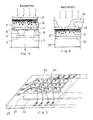
- a conventional example of such radiation image detectors consists, as is shown in Figure 5, essentially of a slender radiation-detective semiconductor base 21 having its radiation image receiving front surface provided with one or a few arrays of pixel-corresponding signal takeout electrodes 23 and its back surface plated with a common bias electrode 22.
- arrayed pixel-corresponding unit radiation sensors are formed, each between the common bias electrode 22 and each of the pixel-corresponding signal takeout electrodes 23.
- the semiconductor base 21 on which are thus formed many pixel-corresponding unit radiation sensors is mounted on a terminal board 25 with the signal takeout electrodes 23 wired by their respective lead wires 24 to terminals 26 printed on the marginal portions of the terminal board 25.
- the thus constituted one-dimensionally prolonged radiation image detector is made to scan an imaginary plane on which lies an invisible two-dimensional radiation image to be detected.
- Such a one-dimensional detector can not instantly detect a two-dimensional image and takes a fairly long time for complete detection of one image because of the scanning operation of the detector. Further, a detector moving mechanism is inevitable. These disadvantages can easily be eliminated or reduced, in principle, by making the detector enlarged two-dimensionally so that it may entirely or partially cover the area of a radiation image to be detected, though in the case of a partially covering detector an image detection operation is necessarily repeated a few times with the detector displaced to complete the detection of one radiation image.
- the conventional detector of this type has a disadvantage that the radiation photons falling on the clearances left among the signal takeout electrodes 23 cannot be efficiently converted to electrical signals, because most of the electric carriers Q created by such photons are, as is schematically illustrated in Figure 6, substantially out of carrier acceleration fields developed between the common bias electrode 22 and the signal takeout electrodes 23, and so vanish without contributing to image signals.
- An object of the present invention is to provide a large-surfaced two-dimensional radiation image detector by overcoming the above described difficulties involved in two-dimensionally enlarging the conventional radiation image detector consisting of many pixel-corresponding unit radiation sensors.
- Another object of the present invention is to make such a two-dimensional radiation image detector capable of making use of all the electric carriers created by the incident photons including those falling on the portions corresponding to the clearances left among the signal takeout electrodes.
- a further object of the present invention is to provide a method of manufacturing such a two-dimensional radiation image detector.
- An example of the two-dimensional radiation image detector according to the present invention consists essentially of a radiation sensitive semiconductor plate having its one surface provided with a common bias electrode and its other surface provided with a plurality of pixel-corresponding signal takeout electrodes having thereon their respective bumps for leading out electric signals from the signal takeout electrodes. Further, the signal takeout electrodes, with the bumps excluded, and the clearances left among the signal takeout electrodes, are coated with a passivation film.
- the bumps provided on the signal takeout electrodes are, by means of a flip-chip joining technique, soldered to corresponding pads which are arranged on a separately prepared base plate. The pads are electrically led toward the edges of the base plate by their respective lead circuits printed on the same base plate. Electric image signals outputted from the signal takeout electrodes are thus led out to an external electronic circuit system through the pads and the accompanying printed lead circuits.
- the radiation image detector has its main part detachably connected to the base plate.
- any of the radiation image detectors according to the present invention is used with the common bias electrode side directed to incident radiation.
- the method of manufacturing the above radiation image detectors which method also belongs to the present invention, comprises a technique of photoprocessing.
- the radiation image detector is advantageously free from a large number of lead wires running over the signal takeout electrodes.
- all of the electric carriers created within a shallow depth of the semiconductor plate are taken out as image signals (refer to Figure 4).
- a radiation image detector as an embodiment of the present invention consists essentially of a radiation sensitive semiconductor plate 1 having its upper surface plated with a common bias electrode 2 and its lower surface plated with a plurality of pixel-corresponding signal takeout electrodes 3 having at their centres their respective bumps 4. Though the lower surface is further coated with a passivation film 7 with the bumps 4 excluded and the bumps 4 are fixed to the electrodes 3 with a gold layer 8 interposed, not all of these are shown in Figure 1. Their details are best shown in Figure 2 to be mentioned later.
- the radiation image detector is made up of many radiation sensors, each comprising the common bias electrode 1 and a respective pixel-corresponding signal takeout electrode 3, with the semiconductor plate 2 interposed therebetween.
- the radiation image detector has the bumps 4 made to detachably come into contact with the pads 6, but the present invention can be embodied also with the base plate fixedly combined with the radiation image detector into one body by soldering the bumps 4 to the pads 6.
- the bumps 4 themselves are preferably made of solder.
- any of them is expected to be applied with the common bias electrode side directed to the incident radiation which gives a radiation image to be detected.
- the radiation image detector not only is free from complicatedly intertwined lead wires which, wired over the signal takeout electrodes, may cause short-circuit troubles, but also has an advantage that all of the dense electric carriers Q generated in a shallow depth just below the common bias plate 2 are substantially fully converted to electric signals, because the electric fields developed between the common bias electrode 2 and the signal takeout electrodes 3, as is easily supposed from Figure 4, show a continuous distribution along the surface of the common bias electrode 2.
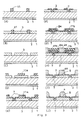
- a photoresist emulsion is applied to the upper surface of a GaAs, CdTe or the like compound semiconductor plate 1 having its lower surface plated with a common bias electrode 2 of gold, platinum, nickel or aluminium, and then the emulsion is photo-processed so as to leave a photoresist film 11 there except for portions where signal takeout electrodes are to be deposited (step A).
- step B nickel is deposited on the semiconductor plate 1 by means of non-electrolytic plating to form signal takeout electrodes 3 (step B).
- the non-electrolytic nickel plating method can of course be replaced by a nickel evaporating method.
- step C the remaining photoresist film 11 is removed by dissolving it with a suitable solvent.
- step D a photoresist emulsion is again applied covering the signal takeout electrodes 3 and the clearances left among them, and then photo-processed so as to leave photoresist films 11a on the signal takeout electrodes 3 and their respective central portions (step D), where signal lead-out bumps are to be finally fixed by means of electroplating.
- a protective passivation film 7 of silicon oxide or silicon nitride is deposited thereon by evaporation or by an electron cyclotron resonance plasma CVD method, covering the semuconductor plate 1, signal takeout electrodes 3 and their respective photoresist films 11a (step E).
- the photoresist films 11a are dissolved with a solvent, and the photoresist films 11a removed to lift off parts of passivation film 7 deposited thereon.
- the passivation film 7 is left only on the areas except for the central portions of the signal takeout electrodes 3 (step F). These central portions are just the above mentioned bump fixing portions.
- a photoresist film 11b is laid only on the remaining passivation films 7 by means of a photo-processing method with their marginal portions excluded, and then as thin a continuous gold layer 8a as possible is deposited thereon by means of evaporation on all the surface of the photoresist film 1lb and the so far exposed (central) portions of the signal takeout electrodes 3 (step G).
- step H soldering metal is accumulated on the recessed portions by means of electroplating with the gold layer 8a used as an electrode to form there pre-bump solder protrusions 4a (step H).
- the photoresist film 11c, the gold layer 8a and the photoresist film 11b are successively removed by means of dissolving the photo resist films and lifting off the gold layer (step I). Since the gold layer 8a is very thin as mentioned above, it can be lifted off relatively easily either by dissolving the photo resist films with a supersonic wave applied or by partially tearing the gold layer 8a mechanically with a photoresist dissolving solvent sprayed.
- step J After the solder protrusions 4a have been thus exposed, temperature is raised to the melting point of the solder, and the solder protrusions melt to form solder beads as the signal lead-out bumps 4 (step J).
- the gold layer 8a employed in the above process can be replaced with any other metal layer, if it is of a metal resistant to electrolytic solution used in the electroplating of solder.
- silver, copper or aluminium also is usable.
- the metal layer may be formed as a multi-layer made by combining silver, copper or aluminium with nickel, chromium or aluminium.
- the radiation image detector main part thus constituted is then combined with a separately prepared base plate 5 (as shown in Figure 2) on which are provided a two-dimensional array of pads 6 corresponding to the signal lead-out bumps 4.
- the bumps 4 of the detector main are solder-joined to the corresponding pads 6 of the base plate 5 by means of a flip-chip joining technique.
- an embodiment of the present invention has the detector main part detachably combinable with the base plate, without solder-joining the bumps 4 to the pads 6.
- the bumps 4 it is desirable to constitute the bumps 4 with any other suitable metal that is not as soft as a solder metal, but wear-resistant and somewhat elastic.
Landscapes
- Measurement Of Radiation (AREA)
Applications Claiming Priority (2)
| Application Number | Priority Date | Filing Date | Title |
|---|---|---|---|
| JP19788489 | 1989-07-29 | ||
| JP197884/89 | 1989-07-29 |
Publications (2)
| Publication Number | Publication Date |
|---|---|
| EP0415541A1 true EP0415541A1 (de) | 1991-03-06 |
| EP0415541B1 EP0415541B1 (de) | 1994-10-05 |
Family
ID=16381902
Family Applications (1)
| Application Number | Title | Priority Date | Filing Date |
|---|---|---|---|
| EP90307957A Expired - Lifetime EP0415541B1 (de) | 1989-07-29 | 1990-07-20 | Halbleiterstrahlungsbilddetektor und sein Herstellungsverfahren |
Country Status (2)
| Country | Link |
|---|---|
| EP (1) | EP0415541B1 (de) |
| DE (1) | DE69013104T2 (de) |
Cited By (19)
| Publication number | Priority date | Publication date | Assignee | Title |
|---|---|---|---|---|
| FR2689684A1 (fr) * | 1992-04-01 | 1993-10-08 | Commissariat Energie Atomique | Dispositif de micro-imagerie de rayonnements ionisants. |
| FR2693033A1 (fr) * | 1992-06-30 | 1993-12-31 | Commissariat Energie Atomique | Dispositif d'imagerie de grande dimension. |
| FR2738705A1 (fr) * | 1995-09-07 | 1997-03-14 | Sagem | Dispositif capteur electromecanique et procede de fabrication d'un tel dispositif |
| GB2319394A (en) * | 1996-12-27 | 1998-05-20 | Simage Oy | Bump-bonded semiconductor imaging device |
| US5834849A (en) * | 1996-02-13 | 1998-11-10 | Altera Corporation | High density integrated circuit pad structures |
| GB2332562A (en) * | 1997-12-18 | 1999-06-23 | Simage Oy | Hybrid semiconductor imaging device |
| EP1001469A3 (de) * | 1995-11-29 | 2000-09-06 | Simage Oy | Herstellung von Kontakten auf Halbleitersubstraten für Strahlungsdetektoren und Bildaufnahmevorrichtungen |
| WO2001004962A3 (en) * | 1999-07-13 | 2001-06-28 | Simage Oy | Forming contacts on semiconductor substrates for radiation detectors and imaging devices |
| EP1041618A4 (de) * | 1998-09-30 | 2001-08-22 | Seiko Epson Corp | Halbleiteranordnung und verfahren zu diesen herstellung, leiterplatte und elektronische anlage |
| US6410922B1 (en) | 1995-11-29 | 2002-06-25 | Konstantinos Evangelos Spartiotis | Forming contacts on semiconductor substrates for radiation detectors and imaging devices |
| WO2004104635A1 (de) * | 2003-05-20 | 2004-12-02 | Fraunhofer-Gesellschaft zur Förderung der angewandten Forschung e.V. | Anordnung zur detektion von röntgenstrahlung und verfahren zu deren herstellung |
| US7132637B2 (en) | 2002-03-03 | 2006-11-07 | Interon As | Pixel sensor array having a layer of sensor material grown on a pre-fabricated wafer and method of manufacture thereof |
| WO2008015450A1 (en) * | 2006-08-03 | 2008-02-07 | Radiation Watch Limited | Method of forming a passivation layer on a surface of a high-energy radiation detector substrate and a high-energy radiation substrate |
| CN100502024C (zh) * | 2004-07-30 | 2009-06-17 | 索尼株式会社 | 半导体模块、摄像机及摄像机的制造方法 |
| US7767487B2 (en) | 2002-10-23 | 2010-08-03 | Ipl Intellectual Property Licensing Limited | Formation of contacts on semiconductor substrates |
| US7872237B2 (en) | 2002-10-25 | 2011-01-18 | Ipl Intellectual Property Licensing Limited | Circuit substrate and method |
| US8169522B2 (en) | 1994-06-01 | 2012-05-01 | Siemens Aktiengesellschaft | Imaging devices, systems and methods |
| EP2388622A3 (de) * | 2002-02-15 | 2014-11-05 | Varian Medical Systems, Inc. | Röntgenbildgebungsvorrichtung |
| US9029793B2 (en) | 1998-11-05 | 2015-05-12 | Siemens Aktiengesellschaft | Imaging device |
Families Citing this family (3)
| Publication number | Priority date | Publication date | Assignee | Title |
|---|---|---|---|---|
| US6784463B2 (en) | 1997-06-03 | 2004-08-31 | Lumileds Lighting U.S., Llc | III-Phospide and III-Arsenide flip chip light-emitting devices |
| DE10332333B4 (de) * | 2003-07-16 | 2006-08-03 | Siemens Ag | Detektormodul |
| DE102006046314A1 (de) * | 2006-09-29 | 2008-04-03 | Siemens Ag | Strahlungsdirektkonvertermodul und Strahlungsdirektkonverter |
Citations (2)
| Publication number | Priority date | Publication date | Assignee | Title |
|---|---|---|---|---|
| US4661192A (en) * | 1985-08-22 | 1987-04-28 | Motorola, Inc. | Low cost integrated circuit bonding process |
| US4670653A (en) * | 1985-10-10 | 1987-06-02 | Rockwell International Corporation | Infrared detector and imaging system |
-
1990
- 1990-07-20 EP EP90307957A patent/EP0415541B1/de not_active Expired - Lifetime
- 1990-07-20 DE DE69013104T patent/DE69013104T2/de not_active Expired - Fee Related
Patent Citations (2)
| Publication number | Priority date | Publication date | Assignee | Title |
|---|---|---|---|---|
| US4661192A (en) * | 1985-08-22 | 1987-04-28 | Motorola, Inc. | Low cost integrated circuit bonding process |
| US4670653A (en) * | 1985-10-10 | 1987-06-02 | Rockwell International Corporation | Infrared detector and imaging system |
Non-Patent Citations (5)
| Title |
|---|
| 5TH IEEE/CHMT INTERNATIONAL ELECTRONIC MANUFACTURING TECHNOLOGY SYMPOSIUM 10 October 1988, LAKE BUENA VISTA, FL, USA pages 23 - 27; K.HATADA ET AL.: "A NEW LSI BONDING TECHNOLOGY "MICRON BUMP BONDING ASSEMBLY TECHNOLOGY"" * |
| IEEE TRANSACTIONS ON PARTS, HYBRIDS AND PACKAGING. vol. 11, no. 4, December 1975, NEW YORK US pages 312 - 315; D.A.GORSKI ET AL.: "FLIP-CHIP HEADER FOR IR DETECTOR ARRAYS OPERATING AT CRYOGENIC TEMPERATURES" * |
| PATENT ABSTRACTS OF JAPAN vol. 11, no. 217 (E-523)(2664) 14 July 1987, & JP-A-62 35634 (HITACHI LTD) 16 February 1987, * |
| PATENT ABSTRACTS OF JAPAN vol. 9, no. 61 (E-303)(1784) 19 March 1985, & JP-A-59 198769 (FUJI DENKI SEIZO K.K.) 10 November 1984, * |
| Proceedings of MELECON'83 Mediterranean Electrotechnical Conference 24 May 1983, ATHENS, GREECE pages 1 - 2; G.GHIONE ET AL.: "COPLANAR LINES IN GaAs HYBRID STRUCTURES : INFLUENCE OF FLIP-CHIP INSERTION" * |
Cited By (27)
| Publication number | Priority date | Publication date | Assignee | Title |
|---|---|---|---|---|
| FR2689684A1 (fr) * | 1992-04-01 | 1993-10-08 | Commissariat Energie Atomique | Dispositif de micro-imagerie de rayonnements ionisants. |
| FR2693033A1 (fr) * | 1992-06-30 | 1993-12-31 | Commissariat Energie Atomique | Dispositif d'imagerie de grande dimension. |
| EP0577487A1 (de) * | 1992-06-30 | 1994-01-05 | Commissariat A L'energie Atomique | Bildaufnehmer für ionisierende Strahlung |
| US5391881A (en) * | 1992-06-30 | 1995-02-21 | Commissariat A L'energie Atomique | Ionizing radiation imaging device |
| US8169522B2 (en) | 1994-06-01 | 2012-05-01 | Siemens Aktiengesellschaft | Imaging devices, systems and methods |
| FR2738705A1 (fr) * | 1995-09-07 | 1997-03-14 | Sagem | Dispositif capteur electromecanique et procede de fabrication d'un tel dispositif |
| EP1001469A3 (de) * | 1995-11-29 | 2000-09-06 | Simage Oy | Herstellung von Kontakten auf Halbleitersubstraten für Strahlungsdetektoren und Bildaufnahmevorrichtungen |
| US6410922B1 (en) | 1995-11-29 | 2002-06-25 | Konstantinos Evangelos Spartiotis | Forming contacts on semiconductor substrates for radiation detectors and imaging devices |
| US6215123B1 (en) | 1995-11-29 | 2001-04-10 | Simage Oy | Forming contacts on semiconductor substrates, radiation detectors and imaging devices |
| US5834849A (en) * | 1996-02-13 | 1998-11-10 | Altera Corporation | High density integrated circuit pad structures |
| GB2319394B (en) * | 1996-12-27 | 1998-10-28 | Simage Oy | Bump-bonded semiconductor imaging device |
| US5952646A (en) * | 1996-12-27 | 1999-09-14 | Simage Oy | Low temperature bump-bonding semiconductor imaging device |
| GB2319394A (en) * | 1996-12-27 | 1998-05-20 | Simage Oy | Bump-bonded semiconductor imaging device |
| GB2332562B (en) * | 1997-12-18 | 2000-01-12 | Simage Oy | Hybrid semiconductor imaging device |
| GB2332562A (en) * | 1997-12-18 | 1999-06-23 | Simage Oy | Hybrid semiconductor imaging device |
| US6410366B1 (en) | 1998-09-30 | 2002-06-25 | Seiko Epson Corporation | Semiconductor device and manufacturing method thereof, circuit board and electronic equipment |
| EP1041618A4 (de) * | 1998-09-30 | 2001-08-22 | Seiko Epson Corp | Halbleiteranordnung und verfahren zu diesen herstellung, leiterplatte und elektronische anlage |
| US9029793B2 (en) | 1998-11-05 | 2015-05-12 | Siemens Aktiengesellschaft | Imaging device |
| WO2001004962A3 (en) * | 1999-07-13 | 2001-06-28 | Simage Oy | Forming contacts on semiconductor substrates for radiation detectors and imaging devices |
| EP2388622A3 (de) * | 2002-02-15 | 2014-11-05 | Varian Medical Systems, Inc. | Röntgenbildgebungsvorrichtung |
| US7132637B2 (en) | 2002-03-03 | 2006-11-07 | Interon As | Pixel sensor array having a layer of sensor material grown on a pre-fabricated wafer and method of manufacture thereof |
| US7767487B2 (en) | 2002-10-23 | 2010-08-03 | Ipl Intellectual Property Licensing Limited | Formation of contacts on semiconductor substrates |
| USRE43948E1 (en) | 2002-10-23 | 2013-01-29 | Siemens Aktiengesellschaft | Formation of contacts on semiconductor substrates |
| US7872237B2 (en) | 2002-10-25 | 2011-01-18 | Ipl Intellectual Property Licensing Limited | Circuit substrate and method |
| WO2004104635A1 (de) * | 2003-05-20 | 2004-12-02 | Fraunhofer-Gesellschaft zur Förderung der angewandten Forschung e.V. | Anordnung zur detektion von röntgenstrahlung und verfahren zu deren herstellung |
| CN100502024C (zh) * | 2004-07-30 | 2009-06-17 | 索尼株式会社 | 半导体模块、摄像机及摄像机的制造方法 |
| WO2008015450A1 (en) * | 2006-08-03 | 2008-02-07 | Radiation Watch Limited | Method of forming a passivation layer on a surface of a high-energy radiation detector substrate and a high-energy radiation substrate |
Also Published As
| Publication number | Publication date |
|---|---|
| DE69013104T2 (de) | 1995-03-23 |
| EP0415541B1 (de) | 1994-10-05 |
| DE69013104D1 (de) | 1994-11-10 |
Similar Documents
| Publication | Publication Date | Title |
|---|---|---|
| EP0415541B1 (de) | Halbleiterstrahlungsbilddetektor und sein Herstellungsverfahren | |
| US7189971B2 (en) | Radiation imaging device and system | |
| EP1411833B1 (de) | Festkörper-röntgendetektormodul und mosaikförmige anordnung desselben, sowie ein bildherstellungsverfahren und eine vorrichtung dazu, die dieses modul verwendt | |
| US4472876A (en) | Area-bonding tape | |
| KR100264479B1 (ko) | 범프전극의 구조와 그 형성방법 | |
| EP0087842B1 (de) | Infrarotstrahlungsdetektoren und deren Herstellung | |
| US6909183B2 (en) | Substrate for an electric component and method for the production thereof | |
| KR20060011845A (ko) | 광검출 장치 | |
| EP1001469A2 (de) | Herstellung von Kontakten auf Halbleitersubstraten für Strahlungsdetektoren und Bildaufnahmevorrichtungen | |
| US3965568A (en) | Process for fabrication and assembly of semiconductor devices | |
| US4206470A (en) | Thin film interconnect for multicolor IR/CCD | |
| US4209347A (en) | Mounting for solar cell | |
| US7355227B2 (en) | Detecting pixel matrix integrated into a charge reader circuit | |
| US6455836B1 (en) | Metallic optical barrier for photo-detector array is also interconnecting electrode | |
| JP4220818B2 (ja) | ホトダイオードアレイおよびその製造方法並びに放射線検出器 | |
| EP1344259B1 (de) | Optoelektronisches bauelement zur umwandlung elektromagnetischer strahlung in einen intensitätsabhängigen fotostrom | |
| JPH10335337A (ja) | 半導体装置及びその製造方法 | |
| JP2005520346A (ja) | 画素センサーのアレーとその製造方法 | |
| JP2006504257A (ja) | 半導体基板上における接点の形成 | |
| US20020131548A1 (en) | Detector for computer tomographs | |
| KR20050116157A (ko) | 포토 다이오드 어레이 및 그 제조 방법 및 방사선 검출기 | |
| EP0561615A2 (de) | Infrarot-Detektoren und ihre Herstellung | |
| US4137625A (en) | Thin film interconnect for multicolor IR/CCD | |
| JP3370663B2 (ja) | 半導体放射線検出素子アレイおよびはんだバンプの作成方法 | |
| EP0281026A2 (de) | Optischer Mosaikdetektor hoher Auflösung und Verfahren zu seiner Herstellung |
Legal Events
| Date | Code | Title | Description |
|---|---|---|---|
| PUAI | Public reference made under article 153(3) epc to a published international application that has entered the european phase |
Free format text: ORIGINAL CODE: 0009012 |
|
| AK | Designated contracting states |
Kind code of ref document: A1 Designated state(s): DE FR GB |
|
| 17P | Request for examination filed |
Effective date: 19910611 |
|
| 17Q | First examination report despatched |
Effective date: 19930312 |
|
| GRAA | (expected) grant |
Free format text: ORIGINAL CODE: 0009210 |
|
| AK | Designated contracting states |
Kind code of ref document: B1 Designated state(s): DE FR GB |
|
| REF | Corresponds to: |
Ref document number: 69013104 Country of ref document: DE Date of ref document: 19941110 |
|
| ET | Fr: translation filed | ||
| PLBE | No opposition filed within time limit |
Free format text: ORIGINAL CODE: 0009261 |
|
| STAA | Information on the status of an ep patent application or granted ep patent |
Free format text: STATUS: NO OPPOSITION FILED WITHIN TIME LIMIT |
|
| 26N | No opposition filed | ||
| REG | Reference to a national code |
Ref country code: GB Ref legal event code: 746 Effective date: 20000525 |
|
| REG | Reference to a national code |
Ref country code: FR Ref legal event code: D6 |
|
| REG | Reference to a national code |
Ref country code: GB Ref legal event code: IF02 |
|
| PGFP | Annual fee paid to national office [announced via postgrant information from national office to epo] |
Ref country code: GB Payment date: 20050720 Year of fee payment: 16 |
|
| PG25 | Lapsed in a contracting state [announced via postgrant information from national office to epo] |
Ref country code: GB Free format text: LAPSE BECAUSE OF NON-PAYMENT OF DUE FEES Effective date: 20060720 |
|
| GBPC | Gb: european patent ceased through non-payment of renewal fee |
Effective date: 20060720 |
|
| PGFP | Annual fee paid to national office [announced via postgrant information from national office to epo] |
Ref country code: DE Payment date: 20070712 Year of fee payment: 18 |
|
| PGFP | Annual fee paid to national office [announced via postgrant information from national office to epo] |
Ref country code: FR Payment date: 20070710 Year of fee payment: 18 |
|
| PG25 | Lapsed in a contracting state [announced via postgrant information from national office to epo] |
Ref country code: DE Free format text: LAPSE BECAUSE OF NON-PAYMENT OF DUE FEES Effective date: 20090203 |
|
| REG | Reference to a national code |
Ref country code: FR Ref legal event code: ST Effective date: 20090331 |
|
| PG25 | Lapsed in a contracting state [announced via postgrant information from national office to epo] |
Ref country code: FR Free format text: LAPSE BECAUSE OF NON-PAYMENT OF DUE FEES Effective date: 20080731 |