EP0415852A2 - Eingangsschaltung für CCD-Verzögerungsleitung - Google Patents
Eingangsschaltung für CCD-Verzögerungsleitung Download PDFInfo
- Publication number
- EP0415852A2 EP0415852A2 EP90402413A EP90402413A EP0415852A2 EP 0415852 A2 EP0415852 A2 EP 0415852A2 EP 90402413 A EP90402413 A EP 90402413A EP 90402413 A EP90402413 A EP 90402413A EP 0415852 A2 EP0415852 A2 EP 0415852A2
- Authority
- EP
- European Patent Office
- Prior art keywords
- delay line
- register
- input
- ccd delay
- ccd
- Prior art date
- Legal status (The legal status is an assumption and is not a legal conclusion. Google has not performed a legal analysis and makes no representation as to the accuracy of the status listed.)
- Granted
Links
Images


Classifications
-
- G—PHYSICS
- G11—INFORMATION STORAGE
- G11C—STATIC STORES
- G11C19/00—Digital stores in which the information is moved stepwise, e.g. shift registers
- G11C19/28—Digital stores in which the information is moved stepwise, e.g. shift registers using semiconductor elements
- G11C19/282—Digital stores in which the information is moved stepwise, e.g. shift registers using semiconductor elements with charge storage in a depletion layer, i.e. charge coupled devices [CCD]
- G11C19/285—Peripheral circuits, e.g. for writing into the first stage; for reading-out of the last stage
-
- G—PHYSICS
- G11—INFORMATION STORAGE
- G11C—STATIC STORES
- G11C27/00—Electric analogue stores, e.g. for storing instantaneous values
- G11C27/04—Shift registers
Definitions
- the present invention generally relates to a charge-coupled device (i.e., CCD) delay device which is used to delay an analog signal such as a video signal or the like and is, more particularly directed to an input circuit for a CCD delay line.
- CCD charge-coupled device
- a modern television receiver utilizes a CCD delay device formed of a CCD delay line to delay an analog signal such as a video signal.
- a CCD delay device formed of a CCD delay line to delay an analog signal such as a video signal.
- an input signal of large level e.g., level slightly higher than the level corresponding to the maximum amount of charge that the CCD delay line can handle
- an overflow of charges occurs in a charge transfer portion of the CCD delay line, which leads to various disadvantages.
- the maximum amount of charge handled by the CCD delay line can vary depending on the CCD delay line characteristics, so that the limiting level of the limiting circuit must be adjusted in concert with the CCD delay lines, which is very inconvenient.
- the CCD delay line has temperature characteristic, so that when the temperature is changed, the level K controlled by the limiting circuit and the maximum acceptable charge amount inputted to the CCD delay line will diverge, so creating a difference. This difference will cause an overflow of charge if the change of temperature is too large.
- an input circuit for a charge-coupled device (CCD) delay line is comprised of a semiconductor substrate, a CCD delay line formed on the semiconductor substrate, first and second registers each having substantially the same maximum charge handling capacity as the CCD delay line and formed on the semiconductor substrate, an input portion of the first register having substantially the same structure as that of the CCD delay line, output portions of the first and second registers having substantially the same structure each other, a control circuit for controlling the second register so that an output signal from the second register becomes a signal corresponding to the maximum charge handling capacity, a comparator circuit for comparing output signals of the first and second registers, wherein an output signal of the comparator circuit is fed back to an input source of the input portion of the first register so that the output signal from the first register becomes equal to the output signal from the second register, a high level clock signal voltage being supplied to an input gate of the first register and a voltage of the input source of the first register being supplied to an input source of an input portion of the CCD delay line.
- Fig. 1 shows a cross-sectional view of a first embodiment of the input circuit for a CCD delay line according to the present invention
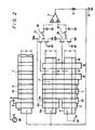
- Fig. 2 shows a plan view thereof.
- reference numeral 4 designates a P-type silicon semiconductor substrate.
- the P-type silicon semiconductor substrate 4 has formed thereon a CCD delay line 1 through which a signal charge is transferred.
- the length of the CCD delay line 1 is determined in accordance with a delay time.
- a first register 2 having the same width a as the width a of the CCD delay line 1 and which has a predetermined length
- a second register 3 having the same width a and the same length as the first register 2.
- the widths a of the first and second registers 2 and 3 are selected to be equal to the width a of the CCD delay line 1 as mentioned above, and the maximum amounts of charge handled by the first and second registers 2 and 3 and the CCD delay line 1 are made equal.
- the CCD delay line 1 in this embodiment is formed of an n-channel BCCD (buried-channel CCD) of a double layer electrode structure which is operated in a two-phase system.
- the CCD delay line 1 and the first and second registers 2 and 3 are each formed of an n layer formed on the surface of the P-type silicon semiconductor substrate 4.
- An input source region 6 of n+ layer is formed on one end of the input portion of the CCD delay line 1.
- the transfer electrodes 10 and 11 forming the first and second layers and the first and second input gate electrodes 8 and 9 are electrically insulated by interlayer insulating layers 12 made of SiO2.
- An input portion of the first register 2 is constructed substantially the same as that of the CCD delay line 1.
- the input portion of the first register 2 has formed at one end thereof an input source region 6a which is identical to the input source region 6 of the CCD delay line.
- the first register 2 has formed thereon through an SiO2 insulating layer 7, first and second input gate electrodes 8a and 9a, each of which is made of impurity-doped polycrystalline silicon, a transfer electrode 10a forming a first layer and a transfer electrode 11a forming a second layer.
- the transfer electrodes 10a and 11a forming the first and second layers and the first and second input gate electrodes 8a and 9a are electrically insulated by interlayer insulating layers 12 made of SiO2.
- the transfer electrodes 10a and 11a of the first and second layers are extended on the second register 3 so as to be usable as transfer electrodes of first and second layers of the second register 3.
- An output portion of the first register 2 has formed on the other end thereof a floating diffusion layer 13 made of an n+ layer. Further, a pre-charge drain region 14 is formed in the P-type silicon semiconductor substrate 4 at its portion distant from the floating diffusion layer 13 by a predetermined spacing.
- the first register 2 has formed thereon an output gate electrode 15 and a pre-charge gate electrode 16, each of which is made of impurity-doped polycrystalline silicon. The output gate electrode 15 and the pre-charge gate electrode 16 are extended up to the second register 3 so as to be usable as an output gate electrode and a pre-charge gate electrode of the second register 3.
- An input source region 17 of an n+ layer is formed on the input portion at one end of the second register 3.
- a floating diffusion region 18, which is identical to the floating diffusion region 13 of the first register 2, is formed on the output portion at the other end of the second register 3.
- a pre-charge drain region 19, which is identical to the pre-charge drain region 14 of the first register 2, is formed away from the floating diffusion region 18 by a predetermined spacing.
- the second register 3 has formed thereon transfer electrodes 20 and 21 of first and second layers made of impurity-doped polycrystalline silicon at the positions corresponding to the first and second input gate electrodes 8a and 9a of the first register 2.
- the pre-charge drain regions 14 and 19 of the first and second registers 2 and 3 are used to accumulate charges of the floating diffusion regions 13 and 18 in association with the opening and closing operation of switches 25 and 30 (which will be described later). The accumulation of charges is controlled by the pre-charge gate electrode 16.
- the floating diffusion region 13 of the first register 2 is connected through a source follower transistor 24 formed of metal-oxide-semiconductor field-effect transistors (i.e., MOSFETs) 22 and 23 and the switch 25 to an inverting input terminal - of an operational amplifier circuit 5 which forms a comparing circuit.
- MOSFETs metal-oxide-semiconductor field-effect transistors
- the floating diffusion region 18 of the second register 3 is connected through a source follower transistor 29 formed of MOSFETs 27 and 28 and the switch 30 to a non-inverting input terminal +of the operational amplifier circuit 5 which forms the comparator circuit.
- An output terminal of the operational amplifier circuit 5 is grounded via a series circuit comprising a resistor 31 and a capacitor 32. A junction between the resistor 31 and the capacitor 32 is coupled to the input source region 6a of the first register 2. Thus, a compared output signal from the operational amplifier circuit 5 is fed back to the input source region 6a of the first register 2.
- an input signal source 33 is connected to the second input gate electrode 9 of the CCD delay line 1, and the second input gate electrode 9a of the first register 2 is supplied with a voltage provided when a clock signal is at high level, for example, a power source voltage V DD of 5 Volts.
- the input source region 17 of the second register 3 is coupled with a battery 34 which generates a dc voltage.
- the voltage of the battery 34 is selected to be such that charges equal to the maximum charge handling capacity of the second register 3, - i.e., charges equal to the maximum charge handling capacity of the CCD delay line 1 - can always be transferred to the second register 3.
- the charge transfers of the CCD delay line and the first and second registers 2 and 3 are performed by supplying predetermined two-phase clock signals o1 and o2 to the pairs of the transfer electrodes 10, 10a and 20 of the first layer and the transfer electrodes 11, 11a and 21 of the second layer in a predetermined sequential order.
- the transfer direction of charges is determined by changing a concentration of impurities in the semiconductor substrate 4 beneath the transfer electrodes 10, 10a, 20 of the first layer and the transfer electrodes 11, 11a, 21a of the second layer to form asymmetric potential wells.
- the voltage supplied to the input source region 6a of the first register 2 is supplied to the input source region 6 of the CCD delay line 1.
- the first input gate electrodes 8 and 8a of CCD delay line 1 and the first register 2 are supplied with the clock signal o2 whose phase is different from that of the clock signal o1 supplied to the transfer electrodes 11, 10, 11a and 10a of the output side of the second input gate electrodes 9 and 9a.
- the input circuit for the CCD delay line of this embodiment is constructed as set out above. According to this embodiment, a charge transferred through the second register 3 and arriving at the floating diffusion region 18 is converted into a voltage by the source follower transistor 29 and is then sampled and held by the switch 30. As described above, the operational amplifier circuit 5 is supplied at the non-inverting input terminal + thereof with the voltage of magnitude corresponding to the maximum charge handling capacity of the second register 3, i.e. the voltage of magnitude corresponding to the maximum charge handling capacity of the CCD delay line 1.
- the clock signal o2 is supplied to the first input gate electrode 8a of the first register 2 and the voltage V DD , provided when the clock signals o1 and o2 are at high level, and is supplied to the second input gate electrode 9a, whereby charge is transferred to the first register 2 formed under the transfer electrodes 10a and 11a of the first and second layers. The charge thus transferred is finally brought to the floating diffusion region 13 via the transfer electrodes 10a and 11a forming the first and second layers.
- the transfer electrodes 10a and 11a of the first and second layers and the output gate electrode 15 are made common to the first and second registers 2 and 3, the charge corresponding to the maximum charge handling capacity of the second register 3 is transferred to the floating diffusion region 18 of the second register 3 at the same cycle as when the charge is transferred to the floating diffusion region 13 of the first register 2.
- the charges respectively transferred to the floating diffusion region 13 of the first register 2 and the floating diffusion region 18 of the second register 3 are converted into voltages by the source follower transistors 24 and 29, respectively, and are sampled and then held at the same time slot so that the operational amplifier circuit 5 is supplied at its inverting input terminal - with the voltage of magnitude corresponding to the amount of charge transferred through the first register 2 and at its non-inverting input terminal + with the voltage of magnitude corresponding to the maximum charge handling capacity of the second register 3.
- the operational amplifier circuit 5 generates at its output terminal a feedback voltage corresponding to a difference between the voltages supplied to the inverting input terminal - and the non-inverting input terminal + .
- the amount of charge accumulated in the input source region 6a of the first register 2 is controlled by the feedback voltage from the output terminal of the operational amplifier circuit 5.
- the feedback voltage is generated from the output terminal of the operational amplifier circuit 5 so that the amount of charge transferred through the first register 2 becomes equal to the amount of charge transferred through the second register 3. This feedback voltage is then supplied to the input source region 6a of the first- register 2.
- the amount of charge transferred through the first register 2 is always kept equal to the maximum amount of charge transferred through the second register 3.
- the voltage supplied to the input source region 6a of the first register 2 is supplied to the input source region 6 of the CCD delay line 1, whereby the voltage of the input source region 6 of the CCD delay line 1 is usable as a source for providing the charge quantity corresponding to the maximum charge handling capacity of the first register 2.
- charges in amounts exceeding of the charge handling capacity are inhibited from being supplied to the charge transfer portion of the CCD delay line 1, thereby avoiding the overflow of charge in the charge transfer portion of the CCD delay line 1.
- the input structures of the CCD delay line 2 and the first register 2 are made the same and the output structures of the first and second registers 2 and 3 are also made the same on the common semiconductor substrate 4.
- the input portion of the CCD delay line 1 and the input portion of the first register 2 are both affected in the same fashion, and similarly the output portion of the first register 2 and the output portion of the second register 3 are both affected in the same fashion. Therefore, it is possible to prevent the charges of the charge transfer portion of the CCD delay line 1 from overflowing as a result of the change of temperature.
- the charges transferred to the floating diffusion regions 13 and 18 of the first and second registers 2 and 3 are converted into the voltages by the source follower transistors 24 and 29 and these voltages are compared in level by the operational amplifier circuit 5, which can be modified as follows.
- Fig. 3 shows a modified example of Fig. 1, and in Fig. 3, like parts corresponding to those of Fig. 2 are marked with the same references and shall therefore not be described in detail.
- floating gate electrodes 36 and 37 made of polycrystalline silicon are respectively formed on the first and second registers 2 and 3 via the insulating layer 7, and these floating gate electrodes 36 and 37 are connected to the source follower transistors 24 and 29, respectively.
- a MOSFET 38 is employed as a reset switch, and the potential of the floating gate electrode 36 is controlled by turning ON or OFF this reset switch.
- the charges in the floating gate electrodes 36 and 37 are converted into the voltages by the source follower transistors 24 and 29 and the two voltages are compared in level by the operational amplifier circuit 5 similarly to the manner described above.
- resistors 39 and 40 are respectively connected between the pre-charge drain regions 14, 19 and the voltage source V DD and voltage drops thereacross are compared by the operational amplifier circuit 5.
- the CCD delay line is formed of the n-channel BCCD of double-layer structure which is operated in two-phase system
- the present invention is not limited thereto. It is needless to say that a CCD delay line formed of a surface channel CCD or a CCD delay line formed of three-phase or multi-phase structure CCD delay line can be employed. Further, it is possible to employ a CCD delay line of single electrode structure or a CCD delay line formed of multi-layer electrode structure of more than three-layer.
- the voltage supplied to the input source of the CCD delay line 1 serves as the source for supplying an amount of charges corresponding to the maximum charge handling capacity of the transfer portion of the CCD line 1
- the upper limit of charges transferred to the transfer portion of the CCD delay line 1 corresponds to the maximum charge handling capacity.
- the first and second registers 2 and 3 for determining the voltage of the input source of the CCD delay line 1 are formed on the same semiconductor substrate 4 as used for the CCD delay line 1, the CCD delay line 1 and the first and second registers 2 and 3 are affected by changes in temperature in the same fashion. the change of temperature. Therefore, regardless of the change of temperature, the overflow of charge can be avoided in the charge transfer portion of the CCD delay line 1.
Landscapes
- Solid State Image Pick-Up Elements (AREA)
- Transforming Light Signals Into Electric Signals (AREA)
Applications Claiming Priority (2)
| Application Number | Priority Date | Filing Date | Title |
|---|---|---|---|
| JP1226749A JP2864553B2 (ja) | 1989-09-01 | 1989-09-01 | Ccd遅延装置 |
| JP226749/89 | 1989-09-01 |
Publications (3)
| Publication Number | Publication Date |
|---|---|
| EP0415852A2 true EP0415852A2 (de) | 1991-03-06 |
| EP0415852A3 EP0415852A3 (en) | 1991-07-17 |
| EP0415852B1 EP0415852B1 (de) | 1995-12-06 |
Family
ID=16850009
Family Applications (1)
| Application Number | Title | Priority Date | Filing Date |
|---|---|---|---|
| EP90402413A Expired - Lifetime EP0415852B1 (de) | 1989-09-01 | 1990-08-31 | Eingangsschaltung für CCD-Verzögerungsleitung |
Country Status (4)
| Country | Link |
|---|---|
| US (1) | US5087843A (de) |
| EP (1) | EP0415852B1 (de) |
| JP (1) | JP2864553B2 (de) |
| DE (1) | DE69023988T2 (de) |
Families Citing this family (4)
| Publication number | Priority date | Publication date | Assignee | Title |
|---|---|---|---|---|
| GB9104705D0 (en) * | 1991-03-06 | 1991-04-17 | Lowe John M | Vision system |
| DE69304460T2 (de) * | 1992-06-29 | 1997-03-13 | Murata Manufacturing Co | Driftunterdrückungsschaltung für Gyrometer |
| US5691629A (en) * | 1995-07-13 | 1997-11-25 | The United States Of America As Represented By The Secretary Of The Air Force | Non-volatile power supply having energy efficient DC/DC voltage converters with a small storage capacitor |
| US6924938B2 (en) | 2003-03-19 | 2005-08-02 | Ricoh Company, Ltd. | Zoom lens, camera, and mobile information terminal |
Family Cites Families (2)
| Publication number | Priority date | Publication date | Assignee | Title |
|---|---|---|---|---|
| US4625322A (en) * | 1983-11-18 | 1986-11-25 | Hitachi, Ltd. | Charge coupled device provided with automatic bias-voltage setting means |
| GB2197556B (en) * | 1986-10-01 | 1990-08-29 | Sony Corp | Charge coupled devices |
-
1989
- 1989-09-01 JP JP1226749A patent/JP2864553B2/ja not_active Expired - Lifetime
-
1990
- 1990-08-30 US US07/575,381 patent/US5087843A/en not_active Expired - Lifetime
- 1990-08-31 EP EP90402413A patent/EP0415852B1/de not_active Expired - Lifetime
- 1990-08-31 DE DE69023988T patent/DE69023988T2/de not_active Expired - Fee Related
Also Published As
| Publication number | Publication date |
|---|---|
| US5087843A (en) | 1992-02-11 |
| JP2864553B2 (ja) | 1999-03-03 |
| DE69023988D1 (de) | 1996-01-18 |
| JPH0391250A (ja) | 1991-04-16 |
| DE69023988T2 (de) | 1996-05-30 |
| EP0415852A3 (en) | 1991-07-17 |
| EP0415852B1 (de) | 1995-12-06 |
Similar Documents
| Publication | Publication Date | Title |
|---|---|---|
| US4093872A (en) | Charge coupled device with input for direct injection of signal | |
| EP0020160B1 (de) | Abtast- und Speicherschaltung | |
| EP0321953B1 (de) | Ladungsübertragungsanordnung mit einer verbesserten Ausgangsstufe | |
| JPS6215960B2 (de) | ||
| EP0324456B1 (de) | Ausgangsschaltung einer Ladungsschiebeanordnung | |
| US4627082A (en) | Semiconductor device for obtaining an accurate threshold voltage adjustment | |
| EP0415852B1 (de) | Eingangsschaltung für CCD-Verzögerungsleitung | |
| US4649554A (en) | Charge transfer device having a subdivided channel output region | |
| US4132903A (en) | CCD output circuit using thin film transistor | |
| US5029189A (en) | Input structure for charge coupled devices with controllable input bias | |
| US4584697A (en) | Four-phase charge-coupled device having an oversized electrode | |
| JPH033391B2 (de) | ||
| US4574384A (en) | Signal transfer system using a charge transfer device | |
| EP0241084B1 (de) | Eingangsstufe für CCD-Anordnung | |
| US4374334A (en) | Signal comparator apparatus | |
| KR100272475B1 (ko) | 전하 전송 장치 및 그 구동 방법 | |
| EP0147697A2 (de) | Ladungsgekoppeltes Bauelement mit steuerbarer Gleichstrom-Eingangsspannung | |
| US5336910A (en) | Charge coupled device of high sensitivity and high integration | |
| JP2569501B2 (ja) | 電荷結合装置 | |
| US4140923A (en) | Charge transfer output circuits | |
| US5086440A (en) | Charge coupled device with enhanced input structure | |
| US5612554A (en) | Charge detection device and driver thereof | |
| EP0065438B1 (de) | Mäanderförmige Ladungsverschiebeanordnung | |
| US4255673A (en) | Input charge corrected monolithically integrated charge transfer device (CTD) arrangement | |
| US5177772A (en) | Charge coupled device with enhanced input structure |
Legal Events
| Date | Code | Title | Description |
|---|---|---|---|
| PUAI | Public reference made under article 153(3) epc to a published international application that has entered the european phase |
Free format text: ORIGINAL CODE: 0009012 |
|
| AK | Designated contracting states |
Kind code of ref document: A2 Designated state(s): DE FR GB |
|
| PUAL | Search report despatched |
Free format text: ORIGINAL CODE: 0009013 |
|
| AK | Designated contracting states |
Kind code of ref document: A3 Designated state(s): DE FR GB |
|
| 17P | Request for examination filed |
Effective date: 19911223 |
|
| 17Q | First examination report despatched |
Effective date: 19940223 |
|
| GRAA | (expected) grant |
Free format text: ORIGINAL CODE: 0009210 |
|
| AK | Designated contracting states |
Kind code of ref document: B1 Designated state(s): DE FR GB |
|
| REF | Corresponds to: |
Ref document number: 69023988 Country of ref document: DE Date of ref document: 19960118 |
|
| ET | Fr: translation filed | ||
| PLBE | No opposition filed within time limit |
Free format text: ORIGINAL CODE: 0009261 |
|
| STAA | Information on the status of an ep patent application or granted ep patent |
Free format text: STATUS: NO OPPOSITION FILED WITHIN TIME LIMIT |
|
| 26N | No opposition filed | ||
| REG | Reference to a national code |
Ref country code: GB Ref legal event code: IF02 |
|
| PGFP | Annual fee paid to national office [announced via postgrant information from national office to epo] |
Ref country code: FR Payment date: 20050809 Year of fee payment: 16 |
|
| PGFP | Annual fee paid to national office [announced via postgrant information from national office to epo] |
Ref country code: DE Payment date: 20050825 Year of fee payment: 16 |
|
| PGFP | Annual fee paid to national office [announced via postgrant information from national office to epo] |
Ref country code: GB Payment date: 20050831 Year of fee payment: 16 |
|
| PG25 | Lapsed in a contracting state [announced via postgrant information from national office to epo] |
Ref country code: DE Free format text: LAPSE BECAUSE OF NON-PAYMENT OF DUE FEES Effective date: 20070301 |
|
| GBPC | Gb: european patent ceased through non-payment of renewal fee |
Effective date: 20060831 |
|
| REG | Reference to a national code |
Ref country code: FR Ref legal event code: ST Effective date: 20070430 |
|
| PG25 | Lapsed in a contracting state [announced via postgrant information from national office to epo] |
Ref country code: GB Free format text: LAPSE BECAUSE OF NON-PAYMENT OF DUE FEES Effective date: 20060831 |
|
| PG25 | Lapsed in a contracting state [announced via postgrant information from national office to epo] |
Ref country code: FR Free format text: LAPSE BECAUSE OF NON-PAYMENT OF DUE FEES Effective date: 20060831 |