EP0416121A1 - Imprimante avec enregistrement des gradations des couleurs - Google Patents
Imprimante avec enregistrement des gradations des couleurs Download PDFInfo
- Publication number
- EP0416121A1 EP0416121A1 EP90903957A EP90903957A EP0416121A1 EP 0416121 A1 EP0416121 A1 EP 0416121A1 EP 90903957 A EP90903957 A EP 90903957A EP 90903957 A EP90903957 A EP 90903957A EP 0416121 A1 EP0416121 A1 EP 0416121A1
- Authority
- EP
- European Patent Office
- Prior art keywords
- light emitting
- gradation
- individual recording
- elements
- recording elements
- Prior art date
- Legal status (The legal status is an assumption and is not a legal conclusion. Google has not performed a legal analysis and makes no representation as to the accuracy of the status listed.)
- Granted
Links
Images


Classifications
-
- B—PERFORMING OPERATIONS; TRANSPORTING
- B41—PRINTING; LINING MACHINES; TYPEWRITERS; STAMPS
- B41J—TYPEWRITERS; SELECTIVE PRINTING MECHANISMS, i.e. MECHANISMS PRINTING OTHERWISE THAN FROM A FORME; CORRECTION OF TYPOGRAPHICAL ERRORS
- B41J2/00—Typewriters or selective printing mechanisms characterised by the printing or marking process for which they are designed
- B41J2/435—Typewriters or selective printing mechanisms characterised by the printing or marking process for which they are designed characterised by selective application of radiation to a printing material or impression-transfer material
- B41J2/447—Typewriters or selective printing mechanisms characterised by the printing or marking process for which they are designed characterised by selective application of radiation to a printing material or impression-transfer material using arrays of radiation sources
- B41J2/45—Typewriters or selective printing mechanisms characterised by the printing or marking process for which they are designed characterised by selective application of radiation to a printing material or impression-transfer material using arrays of radiation sources using light-emitting diode [LED] or laser arrays
-
- B—PERFORMING OPERATIONS; TRANSPORTING
- B41—PRINTING; LINING MACHINES; TYPEWRITERS; STAMPS
- B41J—TYPEWRITERS; SELECTIVE PRINTING MECHANISMS, i.e. MECHANISMS PRINTING OTHERWISE THAN FROM A FORME; CORRECTION OF TYPOGRAPHICAL ERRORS
- B41J2/00—Typewriters or selective printing mechanisms characterised by the printing or marking process for which they are designed
- B41J2/52—Arrangement for printing a discrete number of tones, not covered by group B41J2/205, e.g. applicable to two or more kinds of printing or marking process
-
- H—ELECTRICITY
- H04—ELECTRIC COMMUNICATION TECHNIQUE
- H04N—PICTORIAL COMMUNICATION, e.g. TELEVISION
- H04N1/00—Scanning, transmission or reproduction of documents or the like, e.g. facsimile transmission; Details thereof
- H04N1/40—Picture signal circuits
- H04N1/405—Halftoning, i.e. converting the picture signal of a continuous-tone original into a corresponding signal showing only two levels
- H04N1/4055—Halftoning, i.e. converting the picture signal of a continuous-tone original into a corresponding signal showing only two levels producing a clustered dots or a size modulated halftone pattern
- H04N1/4056—Halftoning, i.e. converting the picture signal of a continuous-tone original into a corresponding signal showing only two levels producing a clustered dots or a size modulated halftone pattern the pattern varying in one dimension only, e.g. dash length, pulse width modulation [PWM]
Definitions
- the present invention relates to a printer for gradation recording by the electrophotographic system.
- a printer by the electrophotographic system outputs printing patterns through exposure of photosensitive material and developing and fixing processes.
- an LED printer As a printer of the electrophotographic system, an LED printer has been proposed, in which a plurality of LED elements are used for exposing photosensitive material and these are individually driven depending on printing patterns.
- the LED printer In comparison with a laser parinter, the LED printer is characterized in that a solid state scanning system is employed and mechanical main scanning is not required; since an optical system can be formed in small in size, the total size of apparatus can also be reduced; and progress in semiconductor technology has realized low cost.
- the light emitting period given to each LED element is changed to equalize the light emitting intensity of each LED element.
- the gradation recording in the LED printer has been conducted by changing the light emitting period of each LED element.
- a plurality of LED elements provide fluctuation of light intensity for each LED element and thereby the recording dot size of each LED element generates fluctuation.
- the Japanese Laid-open Patent No. 62-284567 proposes an LED printer which ensures correct concentration gradation by correcting fluctuation of light intensity of LED elements.
- this LED printer is required to increase the number of light emitting pulses per each recording pixel depending on increase of the number of gradation expressions and accuracy of correction for fluctuation and thereby provides a problem that memory capacity becomes extremely large.
- the present invention relates to an electrophotographic printer in which a plurality of individual light emitting elements are arranged in the form of lines, comprising a means for outputting gradation information for each light emitting element, a means for receiving gradation information of individual light emitting element and giving weighted light emitting pattern signal depending on light intensity characteristic information of each light emitting element and a driving means for driving each light emitting element depending on the light emitting pattern.
- the electrophotographic printer of the present invention it is possible that less amount of information is used since the weighted light emitting pattern signals are given, thereby less amount of gradation information and fluctuation correcting information to be expressed are required and memory capacity can also be reduced.
- Fig. 1 is a diagram for explaining a structure of an LED printer
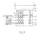
- Fig. 2 is a diagram for explaining a structure of LED head
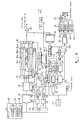
- Fig. 3 is a diagram for explaining a structure of an embodiment
- Fig. 4 is a diagram for explaining control timing signals of an embodiment
- Fig. 5 is a diagram for explaining light quantity correcting ROM
- Fig. 6 is a diagram for explaining the converting operation of LED lighting pattern
- Fig. 7 is a diagram for explaining another embodiment
- Fig. 8 is a diagram for explaining control timing signals of another embodiment.
- Fig. 9 is a diagram for explaining a light quantity correcting ROM in another embodiment.
- Fig. 1 is a diagram for explaining a structure of LED printer.
- a photosensitive drum 10, formed as an image carrier for carrying endless type electrostatic latent image, is charged at the surface thereof to uniform potential (for example, -600 V) by a precharger 11 such as a corona discharger and thereby given the photosensitivity.
- a precharger 11 such as a corona discharger
- This photosensitive drum 10 is formed by stacking an organic photoconductive material and a photoconductive material such as amorphous silicon on a conductive drum.
- this photosensitive drum 10 is irradiated with the information light emitted from LED head 12 depending on the recording pattern to be printed through rod lens array 12a. Thereby, an electrostatic latent image is formed on the photosensitive drum 10 depending on the inforamtion light.
- the electrostatic latent image on the photosensitive drum 10 is developed into a toner image by a developing unit 13 utilizing the double-element developing method using a double-element developer consisting of carrier and toner or the single element developing method.
- This toner image is then transferred to a cut paper PP which is carried in synchronization with the toner image by a tansfer roller 17 in the transfer unit 14 using a corona discharger.
- the cut paper PP having passed the transfer unit 14 is separated from the photosensitive drum 10 by a separating roller 18 and is then sent to a thermal roller fixing unit 19 for fixing the toner image.
- the photosensitive drum 10 is discharged by a photodischarger 15 and thereafter residual toner is removed by a cleaner 16 using a cleaning blade. Thereafter, the operations explained above is repeatedly executed.
- the driver IC 45 is structured by driver elements 42a, ....42n formed by tristate buffers provided corresponding to the LED elemetns 41a, 41b, Vietnamese,41n, latch circuits 43a across43n and a shift register 44 and causes each LED element 41 in the LED chip array 46 to selectively emit the light.
- the driver elements 42a,...42n are connected to a common signal line so that the weighted light emitting enable signal generated as described later can be input thereto.
- the shift register 44 sequentially shifts the serial data transferred for each input of transfer clock and has the number of stages same as the LED element 41.
- the latch circuit 43 inputs the latch signal when n serial data are stored in the shift register 44 and therefore latches a value of shift register 44 in this timing.
- the driver element 42 sets the supply of power for the LED element 41 to the ON or OFF condition, depending on the value latched by the latch circuit 43, during the period wherein the light emitting enable signal is applied.
- Fig. 2 is a diagram for explaining a structure of an embodiment of the LED printer of the present invention.
- the numeral 31 designates an image memory to store the 8-bit gradation image data of the single page to be output for printing; 32, a gradaton decoder which converts the gradation image data read from the image memory 31 to the 3-bit gradation data; 34a, 34b, line buffers for storing 3-bitg gradation data output from the gradation decoder 32; 33, 35, buffer switches which are formed, for example, by a multiplexer.
- the buffer switch 33 selectively input the output of gradation decoder 32 to any one of the line buffers 34a and 34b, while the buffer switch 35 selects an output of line buffer not selected by the buffer switch 33.
- the numeral 50 defines a ROM for storing the fluctuation correcting data which stores fluctuation correcting data corresponding to each LED element 41.
- MPU 100 comprises an X address counter (XADC) 101 provided therein and a Y address counter (YADC) 102 and reads the gradation image data by giving the values of this XADC 101 and YADC 102, namely the dot position address in the X and Y directions to the image memory 31 through the address register 109.
- XADC X address counter
- YADC Y address counter
- XADC 101 is caused to make increment in synchronization with the oacillation clock of the reference clock oscillator 110, while YADC 102 is counted up when there is a carry signal which is output in the timing that XADC 101 becomes the final address of the storing position of lateral direction of image memory 31 (the axial direction of photosensitive drum 10 corresponding to the main scanning direction), namely 4096 in case 4096 LED elements are used as described above and the line clock (Fig. 4(a)) output by the address counter 121 described later is input through the I/O interface 103.
- YADC 102 outputs the carry signal when it reaches the final address of storing position of the vertical direction of image memory 31 (circumferencial direction of photosensitive drum 10 corresponding to the subscanning direction), informing that output of image data as many as one page has complted.
- MPU 100 stores image data sent from the host computer not illustrated which is already received in this timing and outputs image of the next page.
- the image data of each dot position read drom the image memory 31 is applied to the buffer switch 33 after it is converted to the gradation date of 3 bits by the gradation decoder 32.
- MPU 100 outputs the set signal when it starts the operation through the I/O interface 103 to set the T type flipflop 111 and moreover clears the line buffer 34 and resets each counter.
- T type flipflop 111 an output of T type flipflop 111 is input to the buffer switches 33 and 35 and multiplexer 112, the buffer switch 33 is switched to input an output of the gradation decoder 32 to the line buffer 34a, while the buffer switch 35 is switched to select an output from the line buffer 34b and the multiplexer 112 is switched to input the write enable signal WE from the I/O interface 103 to the line buffer 34a.
- the address counter 120 counts up the reference clocks sent from the reference clock oscillator 110 and outputs such count value to the upper bit positions of address register 140 through the AND gate circuit 130.
- a count value of address counter 121 for counting the clocks frequency-divided by the frequency dividers 113 and 114 from the refernece clock of the refrence clock oscillator 110 is set to the lower bit positions of the address register 140.
- the frequency divider 113 outputs the first frequency divided clock by dividing the frequency of the reference clock to the clock of 1/4096 period, while the frequency divider 114 outputs the second frequency divided clock by dividing the frequency of the first frequency divided clock to the clock of 1/5 period.
- the value "4096" of the frequency divider 113 is equal to the number of LED elements 41 in case the refernece clock matches the image data reading period from the image memory 31.
- the period of first frequency divided clock is set to be equal to the period t1 of the subline clock indicated in Fig. 4(d), while the period of second frequency divided clock is set to be equal to the gradation line clock t2 indicated in Fig. 4(b).
- the line buffer 34 is accessed in accordance with the content being set to the address register 140.
- the address counter 120 counts up in synchronization with the gradation image data output from the image memory 31, giving the dot position address for writing or reading data to the line buffer 34, while the address counter 121 gives the gradation line selection address for selecting gradation lines 34 a1 ⁇ 34 a3 in the line buffer 34a and gradation lines 34 b1 ⁇ 34 b3 in the line buffer 34b.
- the gradation data is stored in the predetermined positiono of line buffer 34a in accordance with the address to be set in the address register 140 and the gradation data of the predetermined position of the line buffer 34b is output through the buffer switch 35.
- the counter 122 counts up the first frequency divided clock of the frequency divider 113 and outputs such count value.
- the decoder 150 decodes an output value of the counter 122. Namely, it outputs "0" when an output of counter 122 is “1” or "1" when the output of counter 122 is not "1".
- the AND gate 132 outputs the subline clock of the type in which the second clock (indicated by a broken line) is eliminated as shown in Fig. 4(d).
- the second clock is extracted because it is requested that the duty ratio of the light emitting enable signal must be large.
- the AND gates 130 and 134 do not output the count output of address counter 120 and carry signal when an output of decoder 150 is "0", namely during the periods of second (indicated by the broken line) and third clocks of Fig. 4(d).
- the address counter 123 counts up the subline clock output from the AND gate circuit 132 and outputs such count value. An output of address counter 123 is input to the lower bit position of the address register 141.
- the fluctuation compensating ROM 50 outputs a value in accordance with the fluctuation charcteristic of light intensity of the LED element 41 in the dot position address in synchronization with an output of the gradation data corresponding to the dot position address from the line buffer 34b.
- An output of the address counter 123 is input to the decoder 151 through a delay circuit 180 which delays the subline clock indicated in Fig. 4(d) for the period of t1.
- the decoder 151 selects the monomiultivibrator (MMB) 151 when an output of the address counter 123 is "0", or MMB 162 when an output is “1", or MMB 163 when an output is “2", or MMB 164 when an output is "3".
- MMB monomiultivibrator
- MMB 161 outputs the light emitting enable signal of the light emitting period e1, while MMB 162 outputs the light emitting enable signal of the light emitting period e2, MMB 163 outputs the light emitting enable signal of the light emitting period e3 and MMB 164 outputs the light emitting enabale signal of the light emitting period e4.
- the address counter 123 repeats the countup operation of count value from "0" every time when the address counter 121 counts up and outputs the gradation line clock, the light emitting enable signal indicated by Fig. 4(f) is input to a driver element 42 of LED head through the OR circuit 171.
- the light emitting period e1 has the light emitting time of eight unit time, while the light emitting period e2 the emitting time of four unit time, the light emitting period e3 the emitting time of two unit time and the light emitting period e4 the emitting time of one unit time. Combination of such unit times provides the light emitting time of 0 15 unit times.
- Fig. 5 indicates content of the light quantity compensating ROM 50.
- the light quantity compensating data is stored in the form of 4 bits for every LED element 41 to select the subline for light emitting.
- the light emitting time of eight unit times is set, for the subline 1, the light emitting time of four unit times, for the subline 2, the light emitting time of two unit times and for the subline 3, the light emitting time of one unit time is set, respectively.
- the LED element providing the dot position address 0 executes light emission in the subline 0 and subline 3 and continues light emission during nine unit times in total.
- the LED element providing the dot position address 1 executes light emission in the subline 0 and subline 1 and continues light emission during 12 unit times in total.
- the light emitting time of the LED element having an average light intensity is set to the 12 unit times and light quantity compensation is carried out within the range of the 8 ⁇ 15 unit times.
- the LED element When a voltage is constant, the LED element increases light quantity accurately in proportional to the duration of pulse applied. Accordingly, it is no longer necessary to provide the light quantity value in every gradation level for each LED element of the light quantity compensating ROM 50 and it is enough that a common compensating value for each gradation level is stored in the memory.
- MPU 100 resets each counter through the I/O interface 103 and outputs the write enable signal WE to the multiplexer 112. It moreover applies the addresses indicated by XADC 101 and YADC 102 to the image memory 31 synchronously with the clock of refernece clock generator 110 and inputs the gradation image data read from the image memory 31 to the gradation decoder 32.
- the gradation image data is read synchronously with the reference clock from the reference clock oscillator 110 shown in Fig. 6(a) and the gradation image data "0", “1", “2”,.... are read for each dot position address (0), (1), .... as shown in Fig. 6(b).
- This gradation data is converted to the gradation data of 3 bits by the gradation decoder 32 and is then stored in the line buffer as indicated in Fig. 6(c). Namely, in the gradation data with gradation level "0”, three bits are all "0” and gradation data of gradation level "1” is converted to "100", the gradation data with gradation level "2” is converted to "110".
- the gradation data with gradation level "3" is converted to the light pattern "111" in which three bits are all "1".
- the lighting pattern of gradation line does not allow lighting of the LED element for the gradation level 0, causes the LED element to light during the period of gradation line 0 for gradation level 1, causes the LED element to light during the gradation 0 and 1 for gradation level 2 and causes the LED element to light during the gradation line 0, 1 and 2 for gradation level 3.
- the level "0” is stored to the line buffers 34 a1 ⁇ 34 a3 (or 34 b1 ⁇ 34 b3 ) as shown in Fig. 6(d). Moreover, when the gradation level is "1", the level "1" is stored only to the line buffer 34 a1 (or 34 b1 ) and the level "0" to the other line buffers.
- the dot position address is set to the address register 140 and a count value of the address counter 121 is "0" in this case, the first bit among the gradation data of three bits output from the gradation decoder 32 is stored in the line buffer 34 a1 .
- the other bits are sequentially stored in the storing position in the line buffer 34 a1 corresponding to the dot position address indicated by the count value of address counter 120.
- the other line buffer 34 b1 is selected by the switch 35 and the data of the corresponding position is output to the one input terminal of the AND gate circuit 131.
- the flucturation compensating ROM 50 reads the data "1" stored in the storing position of the dot position address "0" with the subline address "0" and then applies such data to the other input of the AND gate circuit 131. However, since the other input of the AND gate circuit 131 is "0", "0" is output as indicated in Fig. 6(e).
- the carry signal of address counter 120 is input to the counter 124.
- An output of counter 124 is input to the decoder 152, which outputs "1" when the count value is “0” or outputs "0" when count value is “1” ⁇ "4". Accordingly, the AND gate circut 139 outputs the write enable signal only when the first subline clock shown in Fig. 4(b) is output.
- the address counter 120 starts again the countup operation of reference clock generated by the reference clock oscillator 110.
- the decoder 151 causes MMB 161 to carry out the selecting operation and applies the light emitting enable signal of light emitting period e1 with eight unit times to the driver element 42.
- the decoder 151 inputs the count value "1" of the address counter 123 and therefore it selects MMB 162 and drives the LED element 41 by applying the light emitting enable signal of the light emitting period e2 with the four unit times to the driver element 42.
- the gradaton line clock as the second frequency divided clock is input to the address counter 121 from the frequency divider 114. It is then counted up and the count value "1" is set to the address register 140.
- the signal of gradation line 1 is applied to cause the LED element 41 at the dot position addresses "2", “3", etc. of the gradation data of "2" or more to execute the light emitting operation.
- the signal pattern of gradation line "2" is applied, as shown in Fig. 6(g), to the LED element 41 at the dot position address "3" with the gradation of "3” to execute the light emitting operation by repeatedly executing the operations mentioned above.
- the address counter 121 counts up and the carry signal (line clock in Fig. 4(a)) is input to the T type flipflop 111. Therefore, the T type flipflop 111 inverts its output.
- the buffer switch 33 inputs an output of gradation decoder 32 to the line buffer 34b, while the buffer switch 35 selects an output of the line buffer 34a and the multiplexer 112 is switched to apply the write enable signal to the line buffer 34b.
- YADC 102 of MPU 100 counts up and sets the read address to the image memory 31 to read the gradation image data of the next line.
- MPU 100 operates the drivers 190 and 191 through the I/O interface 103 for each output of the first frequency divided clock, namely synchronous with the output timing of clock output from the frequency divider 113 or the timing of the counter 122 for the countup operation and rotatably drives a stepping motor 195 for driving the photosensitive drum 10 and a stepping motor 196 for driving the sheet transfer rollers 32 and 33 for the one subline in the subscanning direction.
- the gradation recording can be realized under the condition that the fluctuation is compensated.
- Fig. 7 is a diagram for explaining a structure of the other embodiment of the LED printer of the present invention.
- numerals 210 and 211 designate line buffers storing gradation image data read from the image memory 31; 220, a light quantity compensating ROM storing the light quantity compensating data of each LED element 41 for every gradation level; 230, an address register setting addresses for making access to the light quantity compensating ROM 220; 231, an address register setting addresses for making access to the line buffers 210, 211; 232, an address counter for counting the reference clock generated by the reference clock oscillator 110; 240, a frequency divider for dividing the reference clock from the reference clock oscillator 110 to the period of 1/4096 and outputting a third frequency divided clock (the clock in the same period as the period t3 of the suline clock shown in Fig.
- 250 a counter for counting the third frequency divided clock
- 260 a decoder outputting "0" only when the count value of counter 250 is "1", namely when the second clock (indicated by the broken line) of Fig. 8(b) is output
- 270, 271 AND gates for inputting an output of the decoder 260 to the one terminal
- the comparator 281 drives the monomultivibrator (MMB) 301 which outputs the light emitting enable signal of 128 unit times when a count value of counter 250 is 0; the comparator 282 drives MMB 302 which outputs the light emitting enable signal of 64 unit times when a count value of the counter 250 is 2; the comparator 283 drives MMB 303 which outpus the light emitting enable signal of 32 unit times when a count value of counter 250 is 3; the comparator 284 drives MMB 304 which outputs the light emitting enable signal of 16 unit times when a count value of counter 250 is 4; the comparator 285 drives MMB 305 which outputs the light emitting enable signal of 8 unit times when a count value of counter 250 is 5; the comparator 286 drives MMB 306 which outputs the light emitting enable signal of 4 unit times when a count value of counter 250 is 6; the comparator 287 drives MMB 307 which outputs the light emitting enable signal of 2 unit times when a count value of counter 250 is 7; the comparator 2
- Fig. 9 is a diagram for indicating content of light quantity compensating ROM in the conversion table.
- the light quantity compensating ROM 220 stores the lighting pattern of subline of each LED element for each gradation level.
- the light emitting time is set in accordance with light intensity of LED element based on the light quantity compensating data, for example, 80 unit times for gradation level 1, 160 unit times for gradation level 2 and 240 unit times for gradation level 3.
- MPU 10 reads the gradation image data from the image memory 31 as in the case of the embodiment of Fig. 3.
- MPU 100 sets the T type flipflop 111 so that the buffer switch 33 selects the buffer memory 210 and therefore the gradation image data is stored in the buffer memory 210.
- the address counter 232 counts up synchronously with the read operation of gradation image data from the image memory 31. Therefore, the write/read address of the line buffers 210, 211 are set to the address register 231 for each gradation image data.
- the gradation image data from the image memory 31 is sequentially stored in the dot position address 0 of the line buffer 210. Moreover, the gradation image data is sequentially read from the dot position address 0 of the line buffer 211. The gradation image data read out is set to the intermediate bit position of address register 230 through the buffer switch 35.
- the dot position address set to the address register 231 and address register 230 are sequentially renewed for each count up of the address counter 232 and the data for each LED element 41 is read.
- the carry signal is applied to the latch circuit 43 as the latch signal, it is then sequentially shifted to the shift register 44 and the data being set is set to the latch circuit 43.
- a count value of counter 240 is input to the comparators 281 ⁇ 288 through the delay circuit 291.
- a count value of counter 250 is "1"
- only the comparator 281 obtains a comparison output, and only MMB 301 is selectively driven and outputs the light emitting enable signal of 128 unit times.
- the address counter 232 outputs the carry signal, a count value of counter 250 becomes “1", an output of decoder 260 becomes “0" and is input to the AND gate circuits 270 and 271. Therefore, outputs of address counter 232 and frequency divider 240 are not input to the address registers 231, 230 and counter 251, the access for the line buffers 210, 211 and light quantity compensating ROM 220 is not carried out and the countup operation of counter 251 is not carried out.
- comparators 281 ⁇ 288 do not obtain the comparison output
- MMBs 302 ⁇ 308 do not operate
- MMB 301 continues output operation of the light emitting enable signal of 128 unit times.
- the gradation recording of the one line is conducted by reading the data sequentially from the light quantity compensating ROM 220 and then setting it to the shift register 44.
- the counter 240 When the counter 251 counts up the value "7" and outputs the carry signal, the counter 240 is reset and is then input to the T type flipflop 111, switching the buffer switches 33, 35 and multiplexer 112.
- MPU 100 causes XADC 101 and YADC 102 to count up and set the count value to the address register in order to read the gradation image data of the next line and also causes the line buffer 211 to store the gradation image data of the next line through the buffer switch 33 by reading it from the image memory 31.
- the gradation recording operation of the next line can be carried out and the gradation recording operation of a single page can be executed.
- the gradation line clock is not provided unlike the first embodiment and light quantity compensation and gradation recording of each LED can be done through combination of the lighting sublines.
- the LED elements have been used as the individual light emitting elements but the present invention is not limited thereto. Namely, the other individual light emitting element can be used and a liquid crystal shutter element in which a plurality of common light sources are arranged like a line may be used.
- the present invention can also be applied to the optical system for exposure of the electgrophotographic printer which realizes color recording.
- the monomultivibrator has been used for outputting the light emitting enable signal of the difference duration, but the present invention is not limited thereto.
- the periodical memory access is conducted by MPU.
- the number of accesses to memory which is different for each subline clock is synchronized with the subline clock for the countup operation, and the light emitting enable signal is output during the period until the count value reaches the predetermined value.
Landscapes
- Engineering & Computer Science (AREA)
- Multimedia (AREA)
- Signal Processing (AREA)
- Physics & Mathematics (AREA)
- Optics & Photonics (AREA)
- Health & Medical Sciences (AREA)
- General Health & Medical Sciences (AREA)
- Toxicology (AREA)
- Printers Or Recording Devices Using Electromagnetic And Radiation Means (AREA)
Abstract
Applications Claiming Priority (3)
| Application Number | Priority Date | Filing Date | Title |
|---|---|---|---|
| JP51218/89 | 1989-03-03 | ||
| JP5121889 | 1989-03-03 | ||
| PCT/JP1990/000270 WO1990009890A1 (fr) | 1989-03-03 | 1990-03-01 | Imprimante avec enregistrement des gradations des couleurs |
Publications (3)
| Publication Number | Publication Date |
|---|---|
| EP0416121A1 true EP0416121A1 (fr) | 1991-03-13 |
| EP0416121A4 EP0416121A4 (fr) | 1994-04-13 |
| EP0416121B1 EP0416121B1 (fr) | 1997-06-04 |
Family
ID=12880787
Family Applications (1)
| Application Number | Title | Priority Date | Filing Date |
|---|---|---|---|
| EP90903957A Expired - Lifetime EP0416121B1 (fr) | 1989-03-03 | 1990-03-01 | Imprimante avec enregistrement des gradations des couleurs |
Country Status (3)
| Country | Link |
|---|---|
| EP (1) | EP0416121B1 (fr) |
| DE (1) | DE69030853T2 (fr) |
| WO (1) | WO1990009890A1 (fr) |
Cited By (2)
| Publication number | Priority date | Publication date | Assignee | Title |
|---|---|---|---|---|
| DE4308496A1 (de) * | 1992-12-09 | 1994-06-16 | Samsung Electronics Co Ltd | Schaltung zum Treiben eines LED-Druckkopfes eines elektrophotographischen Gerätes |
| EP1564006A3 (fr) * | 2004-02-16 | 2008-03-05 | Seiko Epson Corporation | Tête linéaire et machine à formation d'images utilisant cette tête |
Families Citing this family (3)
| Publication number | Priority date | Publication date | Assignee | Title |
|---|---|---|---|---|
| EP0713328B1 (fr) | 1994-11-16 | 1999-09-15 | Konica Corporation | Enregistrement d'images pour matériau photographique à halogénure d'argent, avec correction de non-uniformité entre les éléments d'exposition |
| US7602411B2 (en) * | 2003-06-12 | 2009-10-13 | Oki Data Corporation | Image forming apparatus |
| JP4371322B2 (ja) | 2006-11-06 | 2009-11-25 | 株式会社沖データ | 画像形成装置 |
Family Cites Families (5)
| Publication number | Priority date | Publication date | Assignee | Title |
|---|---|---|---|---|
| US4855760A (en) * | 1987-03-12 | 1989-08-08 | Fuji Photo Film Co., Ltd. | LED array with graduated quantity control |
| JPS63222869A (ja) * | 1987-03-12 | 1988-09-16 | Fuji Photo Film Co Ltd | 画像形成方法 |
| JPS63231939A (ja) * | 1987-03-20 | 1988-09-28 | Fuji Photo Film Co Ltd | 画像形成方法 |
| JPS63312174A (ja) * | 1987-06-15 | 1988-12-20 | Oki Electric Ind Co Ltd | 光プリントヘッドの発光素子駆動方式 |
| JPH06349463A (ja) * | 1993-06-11 | 1994-12-22 | Nissin Electric Co Ltd | 電池容器 |
-
1990
- 1990-03-01 DE DE69030853T patent/DE69030853T2/de not_active Expired - Fee Related
- 1990-03-01 WO PCT/JP1990/000270 patent/WO1990009890A1/fr not_active Ceased
- 1990-03-01 EP EP90903957A patent/EP0416121B1/fr not_active Expired - Lifetime
Cited By (3)
| Publication number | Priority date | Publication date | Assignee | Title |
|---|---|---|---|---|
| DE4308496A1 (de) * | 1992-12-09 | 1994-06-16 | Samsung Electronics Co Ltd | Schaltung zum Treiben eines LED-Druckkopfes eines elektrophotographischen Gerätes |
| DE4308496C2 (de) * | 1992-12-09 | 2002-03-21 | Samsung Electronics Co Ltd | Schaltung und Verfahren zum Treiben eines LED-Druckkopfes eines elektrofotografischen Gerätes |
| EP1564006A3 (fr) * | 2004-02-16 | 2008-03-05 | Seiko Epson Corporation | Tête linéaire et machine à formation d'images utilisant cette tête |
Also Published As
| Publication number | Publication date |
|---|---|
| WO1990009890A1 (fr) | 1990-09-07 |
| DE69030853D1 (de) | 1997-07-10 |
| EP0416121B1 (fr) | 1997-06-04 |
| DE69030853T2 (de) | 1997-09-18 |
| EP0416121A4 (fr) | 1994-04-13 |
Similar Documents
| Publication | Publication Date | Title |
|---|---|---|
| US6088050A (en) | Non-impact recording apparatus operable under variable recording conditions | |
| US5914744A (en) | Apparatus and method of printing with non-uniformity correction of exposure parameters to reduce low spatial frequency printed artifacts | |
| US4835551A (en) | Optical recorder with plural resolution recording | |
| US5751328A (en) | Printer having circuit for providing improved printing quality | |
| JP4723663B2 (ja) | 画像形成方法 | |
| EP0416121A1 (fr) | Imprimante avec enregistrement des gradations des couleurs | |
| JP2004284077A (ja) | Ledプリンタ及び画像形成装置 | |
| JPH07108714A (ja) | 画像形成装置 | |
| US4905027A (en) | Control method and apparatus for optical printer head | |
| JP3280723B2 (ja) | 固体走査ヘッドの駆動装置 | |
| JP2822667B2 (ja) | 階調記録を行なうプリンタ | |
| JPH05500146A (ja) | 2進アーキテクチャプリントヘッドを使用するグレイレベルをプリントする方法及び装置 | |
| JP4360543B2 (ja) | 画像形成装置 | |
| JP2648400B2 (ja) | 画像処理装置 | |
| JP2002283609A (ja) | 画像形成装置 | |
| US5252996A (en) | Electrophotographic recording apparatus and method capable of recording both characters and solid black picture images | |
| JP3522289B2 (ja) | 階調制御回路及びプリンタ | |
| US6195109B1 (en) | Electrophotographic printer | |
| JPH06127025A (ja) | Ledアレイヘッド | |
| JP3561703B2 (ja) | 画像形成装置 | |
| KR960005015B1 (ko) | 프린팅 헤드를 갖는 프린터에서의 계조 표현 방법 및 구동회로 | |
| JPH0516428A (ja) | 光書き込み装置 | |
| JPH05177868A (ja) | 光書込みプリンタ | |
| JPWO1990009890A1 (ja) | 階調記録を行なうプリンタ | |
| JPS62299359A (ja) | 画像露光装置 |
Legal Events
| Date | Code | Title | Description |
|---|---|---|---|
| PUAI | Public reference made under article 153(3) epc to a published international application that has entered the european phase |
Free format text: ORIGINAL CODE: 0009012 |
|
| 17P | Request for examination filed |
Effective date: 19900726 |
|
| AK | Designated contracting states |
Kind code of ref document: A1 Designated state(s): DE FR GB |
|
| A4 | Supplementary search report drawn up and despatched |
Effective date: 19940225 |
|
| AK | Designated contracting states |
Kind code of ref document: A4 Designated state(s): DE FR GB |
|
| 17Q | First examination report despatched |
Effective date: 19950518 |
|
| GRAG | Despatch of communication of intention to grant |
Free format text: ORIGINAL CODE: EPIDOS AGRA |
|
| GRAH | Despatch of communication of intention to grant a patent |
Free format text: ORIGINAL CODE: EPIDOS IGRA |
|
| GRAH | Despatch of communication of intention to grant a patent |
Free format text: ORIGINAL CODE: EPIDOS IGRA |
|
| GRAA | (expected) grant |
Free format text: ORIGINAL CODE: 0009210 |
|
| AK | Designated contracting states |
Kind code of ref document: B1 Designated state(s): DE FR GB |
|
| REF | Corresponds to: |
Ref document number: 69030853 Country of ref document: DE Date of ref document: 19970710 |
|
| ET | Fr: translation filed | ||
| PLBE | No opposition filed within time limit |
Free format text: ORIGINAL CODE: 0009261 |
|
| STAA | Information on the status of an ep patent application or granted ep patent |
Free format text: STATUS: NO OPPOSITION FILED WITHIN TIME LIMIT |
|
| 26N | No opposition filed | ||
| PGFP | Annual fee paid to national office [announced via postgrant information from national office to epo] |
Ref country code: DE Payment date: 20000228 Year of fee payment: 11 |
|
| PGFP | Annual fee paid to national office [announced via postgrant information from national office to epo] |
Ref country code: GB Payment date: 20000301 Year of fee payment: 11 |
|
| PGFP | Annual fee paid to national office [announced via postgrant information from national office to epo] |
Ref country code: FR Payment date: 20000310 Year of fee payment: 11 |
|
| PG25 | Lapsed in a contracting state [announced via postgrant information from national office to epo] |
Ref country code: GB Free format text: LAPSE BECAUSE OF NON-PAYMENT OF DUE FEES Effective date: 20010301 |
|
| GBPC | Gb: european patent ceased through non-payment of renewal fee |
Effective date: 20010301 |
|
| PG25 | Lapsed in a contracting state [announced via postgrant information from national office to epo] |
Ref country code: FR Free format text: LAPSE BECAUSE OF NON-PAYMENT OF DUE FEES Effective date: 20011130 |
|
| REG | Reference to a national code |
Ref country code: FR Ref legal event code: ST |
|
| PG25 | Lapsed in a contracting state [announced via postgrant information from national office to epo] |
Ref country code: DE Free format text: LAPSE BECAUSE OF NON-PAYMENT OF DUE FEES Effective date: 20020101 |