EP0416251A2 - Gesteuertes Verfahren zur Herstellung mehrfacher optischer Rasterfilter - Google Patents
Gesteuertes Verfahren zur Herstellung mehrfacher optischer Rasterfilter Download PDFInfo
- Publication number
- EP0416251A2 EP0416251A2 EP90113621A EP90113621A EP0416251A2 EP 0416251 A2 EP0416251 A2 EP 0416251A2 EP 90113621 A EP90113621 A EP 90113621A EP 90113621 A EP90113621 A EP 90113621A EP 0416251 A2 EP0416251 A2 EP 0416251A2
- Authority
- EP
- European Patent Office
- Prior art keywords
- profile
- optical
- notch
- layer
- thickness
- Prior art date
- Legal status (The legal status is an assumption and is not a legal conclusion. Google has not performed a legal analysis and makes no representation as to the accuracy of the status listed.)
- Granted
Links
- 238000000034 method Methods 0.000 title claims abstract description 121
- 238000004519 manufacturing process Methods 0.000 title abstract description 5
- 230000003287 optical effect Effects 0.000 claims abstract description 112
- 230000008569 process Effects 0.000 claims abstract description 87
- 238000000151 deposition Methods 0.000 claims abstract description 57
- 238000004422 calculation algorithm Methods 0.000 claims abstract description 37
- 239000000758 substrate Substances 0.000 claims abstract description 31
- 238000012544 monitoring process Methods 0.000 claims description 30
- 239000000463 material Substances 0.000 claims description 29
- GQPLMRYTRLFLPF-UHFFFAOYSA-N Nitrous Oxide Chemical compound [O-][N+]#N GQPLMRYTRLFLPF-UHFFFAOYSA-N 0.000 claims description 24
- 239000000376 reactant Substances 0.000 claims description 15
- 239000001272 nitrous oxide Substances 0.000 claims description 12
- 230000005855 radiation Effects 0.000 claims description 12
- 238000013461 design Methods 0.000 claims description 11
- BLRPTPMANUNPDV-UHFFFAOYSA-N Silane Chemical compound [SiH4] BLRPTPMANUNPDV-UHFFFAOYSA-N 0.000 claims description 10
- 229910000077 silane Inorganic materials 0.000 claims description 6
- 238000002834 transmittance Methods 0.000 claims description 6
- 239000002131 composite material Substances 0.000 claims description 5
- 230000000977 initiatory effect Effects 0.000 claims description 2
- 238000005065 mining Methods 0.000 claims 1
- 238000004886 process control Methods 0.000 abstract description 6
- 230000000737 periodic effect Effects 0.000 abstract description 3
- 230000008021 deposition Effects 0.000 description 41
- 239000010408 film Substances 0.000 description 26
- 239000010410 layer Substances 0.000 description 24
- 239000000306 component Substances 0.000 description 16
- 238000012937 correction Methods 0.000 description 13
- 230000009897 systematic effect Effects 0.000 description 13
- 239000000523 sample Substances 0.000 description 12
- VYPSYNLAJGMNEJ-UHFFFAOYSA-N Silicium dioxide Chemical compound O=[Si]=O VYPSYNLAJGMNEJ-UHFFFAOYSA-N 0.000 description 10
- 239000007789 gas Substances 0.000 description 10
- 239000012071 phase Substances 0.000 description 10
- 239000000203 mixture Substances 0.000 description 9
- LIVNPJMFVYWSIS-UHFFFAOYSA-N silicon monoxide Chemical class [Si-]#[O+] LIVNPJMFVYWSIS-UHFFFAOYSA-N 0.000 description 9
- 238000005137 deposition process Methods 0.000 description 7
- 229910052814 silicon oxide Inorganic materials 0.000 description 6
- 238000001228 spectrum Methods 0.000 description 6
- 238000010586 diagram Methods 0.000 description 5
- 235000012239 silicon dioxide Nutrition 0.000 description 5
- 238000007740 vapor deposition Methods 0.000 description 5
- 230000000694 effects Effects 0.000 description 4
- 239000000377 silicon dioxide Substances 0.000 description 4
- 239000010409 thin film Substances 0.000 description 4
- 238000006243 chemical reaction Methods 0.000 description 3
- 239000011248 coating agent Substances 0.000 description 3
- 238000000576 coating method Methods 0.000 description 3
- 229910052681 coesite Inorganic materials 0.000 description 3
- 229910052906 cristobalite Inorganic materials 0.000 description 3
- 230000002452 interceptive effect Effects 0.000 description 3
- 239000002243 precursor Substances 0.000 description 3
- 229910052682 stishovite Inorganic materials 0.000 description 3
- 238000002207 thermal evaporation Methods 0.000 description 3
- 229910052905 tridymite Inorganic materials 0.000 description 3
- IJGRMHOSHXDMSA-UHFFFAOYSA-N Atomic nitrogen Chemical compound N#N IJGRMHOSHXDMSA-UHFFFAOYSA-N 0.000 description 2
- 238000012152 algorithmic method Methods 0.000 description 2
- QVGXLLKOCUKJST-UHFFFAOYSA-N atomic oxygen Chemical compound [O] QVGXLLKOCUKJST-UHFFFAOYSA-N 0.000 description 2
- 230000015572 biosynthetic process Effects 0.000 description 2
- 238000005229 chemical vapour deposition Methods 0.000 description 2
- 239000000470 constituent Substances 0.000 description 2
- 239000013078 crystal Substances 0.000 description 2
- 238000005566 electron beam evaporation Methods 0.000 description 2
- 238000005755 formation reaction Methods 0.000 description 2
- 230000006872 improvement Effects 0.000 description 2
- 230000007246 mechanism Effects 0.000 description 2
- QSHDDOUJBYECFT-UHFFFAOYSA-N mercury Chemical compound [Hg] QSHDDOUJBYECFT-UHFFFAOYSA-N 0.000 description 2
- 239000001301 oxygen Substances 0.000 description 2
- 229910052760 oxygen Inorganic materials 0.000 description 2
- 239000003504 photosensitizing agent Substances 0.000 description 2
- 238000004544 sputter deposition Methods 0.000 description 2
- 238000005019 vapor deposition process Methods 0.000 description 2
- XUIMIQQOPSSXEZ-UHFFFAOYSA-N Silicon Chemical compound [Si] XUIMIQQOPSSXEZ-UHFFFAOYSA-N 0.000 description 1
- 238000002441 X-ray diffraction Methods 0.000 description 1
- 238000013459 approach Methods 0.000 description 1
- 230000008901 benefit Effects 0.000 description 1
- 238000004364 calculation method Methods 0.000 description 1
- 230000008859 change Effects 0.000 description 1
- 238000005234 chemical deposition Methods 0.000 description 1
- 230000003749 cleanliness Effects 0.000 description 1
- 238000004891 communication Methods 0.000 description 1
- 230000032798 delamination Effects 0.000 description 1
- 238000001514 detection method Methods 0.000 description 1
- 239000010432 diamond Substances 0.000 description 1
- 229910003460 diamond Inorganic materials 0.000 description 1
- 239000003989 dielectric material Substances 0.000 description 1
- 238000001017 electron-beam sputter deposition Methods 0.000 description 1
- 238000002474 experimental method Methods 0.000 description 1
- 239000012535 impurity Substances 0.000 description 1
- 238000012423 maintenance Methods 0.000 description 1
- 229910052753 mercury Inorganic materials 0.000 description 1
- 238000002156 mixing Methods 0.000 description 1
- 239000002365 multiple layer Substances 0.000 description 1
- 229910052757 nitrogen Inorganic materials 0.000 description 1
- 230000002085 persistent effect Effects 0.000 description 1
- 238000006552 photochemical reaction Methods 0.000 description 1
- 238000005240 physical vapour deposition Methods 0.000 description 1
- 238000002360 preparation method Methods 0.000 description 1
- 238000012545 processing Methods 0.000 description 1
- 238000010926 purge Methods 0.000 description 1
- 239000010453 quartz Substances 0.000 description 1
- 238000000985 reflectance spectrum Methods 0.000 description 1
- 238000009738 saturating Methods 0.000 description 1
- 150000004756 silanes Chemical class 0.000 description 1
- 229910052710 silicon Inorganic materials 0.000 description 1
- 239000010703 silicon Substances 0.000 description 1
- 230000003595 spectral effect Effects 0.000 description 1
- 238000010561 standard procedure Methods 0.000 description 1
- -1 that is Inorganic materials 0.000 description 1
- 238000002230 thermal chemical vapour deposition Methods 0.000 description 1
- 239000012808 vapor phase Substances 0.000 description 1
Images




Classifications
-
- G—PHYSICS
- G02—OPTICS
- G02B—OPTICAL ELEMENTS, SYSTEMS OR APPARATUS
- G02B5/00—Optical elements other than lenses
- G02B5/20—Filters
-
- G—PHYSICS
- G02—OPTICS
- G02B—OPTICAL ELEMENTS, SYSTEMS OR APPARATUS
- G02B5/00—Optical elements other than lenses
- G02B5/20—Filters
- G02B5/28—Interference filters
- G02B5/289—Rugate filters
-
- C—CHEMISTRY; METALLURGY
- C23—COATING METALLIC MATERIAL; COATING MATERIAL WITH METALLIC MATERIAL; CHEMICAL SURFACE TREATMENT; DIFFUSION TREATMENT OF METALLIC MATERIAL; COATING BY VACUUM EVAPORATION, BY SPUTTERING, BY ION IMPLANTATION OR BY CHEMICAL VAPOUR DEPOSITION, IN GENERAL; INHIBITING CORROSION OF METALLIC MATERIAL OR INCRUSTATION IN GENERAL
- C23C—COATING METALLIC MATERIAL; COATING MATERIAL WITH METALLIC MATERIAL; SURFACE TREATMENT OF METALLIC MATERIAL BY DIFFUSION INTO THE SURFACE, BY CHEMICAL CONVERSION OR SUBSTITUTION; COATING BY VACUUM EVAPORATION, BY SPUTTERING, BY ION IMPLANTATION OR BY CHEMICAL VAPOUR DEPOSITION, IN GENERAL
- C23C16/00—Chemical coating by decomposition of gaseous compounds, without leaving reaction products of surface material in the coating, i.e. chemical vapour deposition [CVD] processes
- C23C16/44—Chemical coating by decomposition of gaseous compounds, without leaving reaction products of surface material in the coating, i.e. chemical vapour deposition [CVD] processes characterised by the method of coating
- C23C16/52—Controlling or regulating the coating process
-
- Y—GENERAL TAGGING OF NEW TECHNOLOGICAL DEVELOPMENTS; GENERAL TAGGING OF CROSS-SECTIONAL TECHNOLOGIES SPANNING OVER SEVERAL SECTIONS OF THE IPC; TECHNICAL SUBJECTS COVERED BY FORMER USPC CROSS-REFERENCE ART COLLECTIONS [XRACs] AND DIGESTS
- Y10—TECHNICAL SUBJECTS COVERED BY FORMER USPC
- Y10S—TECHNICAL SUBJECTS COVERED BY FORMER USPC CROSS-REFERENCE ART COLLECTIONS [XRACs] AND DIGESTS
- Y10S359/00—Optical: systems and elements
- Y10S359/90—Methods
Definitions
- This invention relates generally to the field of optically reflective filters and materials, and, more particularly, to a multiple-notch rugate filter manufactured under a monitored and feedback-controlled deposition process.
- optical sensors An important criterion in the operation of optical sensors is protecting the sensors from possible damage caused by lasers. This protection is referred to as laser hardening and has become necessary due to the widespread use of lasers in industrial and military applications, such as ranging and communications.
- Such protection is needed because laser radiation from friendly or hostile sources, even at lower energy levels, can disable or damage a detection system by saturating or burning out vulnerable components or detector elements. While protecting such systems, low spectral distortion and high see-through are needed to depict an accurate signal.
- a standard method of such protection is a multilayer dielectric reflective filter made of alternating layers of dissimilar materials.
- problems associated with the use of such a discrete multilayer structure is a residual stress in each layer caused by incompatible material properties at the abrupt interfaces. This stress, a problem common to discrete multilayer coatings, can weaken the structure and lead to delamination of the layers.
- abrupt interfaces between dissimilar materials can be sites for dislocation and a high concentration of impurities. These sites can lower the protection capability and power tolerance of the filter if radiation is scattered into the detector or absorbed in the filter.
- Multilayer filters also have inadequate broadband signal transmittance due to the undesired sideband reflectance peaks that arise from the interference effects inherent to the filter design limitations of alternating layer structures.
- Simple reflective multilayer dielectric filters typically consist of alternating layers of two dielectric materials of different refractive indices, which are formed on the surface of a substrate by known deposition techniques, such as chemical vapor deposition, sputtering, or thermal evaporation.
- the optical thickness (in this case, the product of the refractive index and layer thickness) of each layer is chosen to be one quarter of a wavelength of the radiation to be reflected, and such a structure is therefore referred to as a "quarter-wave stack".
- U.S. Patent 4,545,646 to Chern et al. provided a graded-index optical material having continuous gradations in the stoichiometric composition and refractive index as a function of thickness of the material.
- the structure disclosed in U.S. Patent No. 4,545,646 to Chern et al. addressed many of the drawbacks, such as design and performance limitations, in multilayer filters.
- Chern et al. discloses a method whereby the substrate is exposed to first and second vapor phase reactants in predetermined proportions in the presence of radiation to induce a chemical reaction whereby the desired optical material is formed and deposited on the substrate.
- the optical material is deposited in accordance with a predetermined index of refraction.
- the proportion of the reactants to which the substrate is exposed is altered as a function of time in a predetermined and continuous manner which allows the predetermined and continuous variation of the stoichiometric composition and the index of refraction of the deposited material to produce a graded index of refraction which reflects radiation at a given wavelength.
- this single-notch process of Chern et al. it is assumed that the deposition process will occur according to the predetermined pattern. However, no method for insuring the accuracy of the deposition pattern was provided by Chern et al.
- rugate filter fabrication can tolerate errors no greater than about one percent to the original design guide, as disclosed by Southwell et al. in U.S. Patent No. 4,707,611. Therefore, errors greater than one percent need to be compensated as they occur, or else the fabrication process requires termination and starting over.
- the present invention provides an error-compensation method for insuring attainment of a thin-film multiple-notch optical filter deposited on a uniform substrate and having desired properties.
- the thin-film, optically interactive medium has an algorithm-controlled, error-compensated, nearly continuously varying refractive index profile perpendicular to the plane of the substrate.
- the varying refractive index profile of the medium is predominantly reflective at multiple-notches or multiple bands of wavelength.
- the refractive index profile necessary to provide the multiple-notch filter is a combination or superpositioning of sinusoidally varying refractive index profiles, each of which alone provides reflection at a single wavelength or notch.
- the optically interactive medium may comprise a photochemically deposited film of silicon oxides (SiO x ).
- the optical filter medium of this invention is characterized by a continuously varying refractive index profile that is error-compensated according to an algorithmic method of optical coating monitoring, wherein the medium is multiple-sinusoidally phase adjusted during deposition to follow a predetermined and optically measurable pattern.
- the use of the algorithm is novel, and the optical monitoring can be performed with standard, conventional means.
- the optically interactive medium coated upon a uniform substrate, that together with the substrate comprises the multiple-notch rugate filter of this invention, is transmissive to optical radiation except near or at particular notches of wavelength wherein the filter is predominantly reflective, and is referred to herein as "a multiple-notch rugate filter".
- a salient aspect of this multiple-notch rugate filter method is to form this optical medium layer so that the product of the average index of refraction and the component sinusoidal period thicknesses are maintained in such a manner that the desired Bragg reflective condition for each notch is achieved accurately.
- This result is achieved through compensation of errors based on algorithmic actions according to optical monitoring signals during filter deposition.
- the algorithm directs the deposition process to make minor adjustments, either vertically or horizontally, to the depositing index profile in such a manner that the multiple-notch rugate profile that is theoretically desirable is accurately followed in an error-compensated manner.
- the resulting deposited index profile therefore results in practicably realizable multiple-notch rugate filter properties.
- the present algorithmic method of deposition which forms a multiple-notch filter medium that is coated onto a uniform substrate includes the steps of:
- an optical monitoring light beam is directed at the medium so that the light beam is reflected off or transmitted through the medium at a perpendicular or known angle of incidence to an optical thickness detector system, which can be a conventional design similar to that used in monitoring and controlling quarter-wave stack depositions.
- This detector system generates output signals which are a function of the light beam intensity directed into the detector. The output signals are then fed back to the computerized deposition controller in order to adjust the commands of the deposition.
- the target refractive index profile (with respect to growth thickness) is commanded to be adjusted with minor corrective structures that are either horizontal or vertical with respect to whether a target optical thickness is expectedly overdue or prematurely measured.
- the multiple-notch filter medium produced according to the error compensation method of this invention results in a multiple-sinusoidally modulated refractive index profile such that the desired filter is accurately achieved since the notch wavelengths are individually (as Fourier components) the product of two times each sinusoidal period thickness and the average refractive index, according to Bragg's law.
- the relative accuracy of the optical thickness detector system insures the accuracy of the desired multiple Bragg-reflective structures if corrective actions are made often enough (typically four times for the shortest sinusoidal period to compensate for the most severe errors).
- FIG. 1 shows a schematic view of an ideal, triple-notch rugate filter profile taken along the film thickness direction z.
- the final ideal thickness is d
- n m is the surrounding medium index (air)
- n s is the substrate index
- n is the average ideal index.
- a triple-notch will be used for purposes of illustration. It is not, however, intended to limit the present invention to a triple-notch filter, but rather to include any number of notches as may be required.
- the term "notch" is used in its accepted meaning to indicate a nearly zero transmittance band.
- This ideal profile is formed by the superposition of three sinusoidal modulation components, one for each notch according to the following equation.
- ⁇ i each transmittance notch wavelength
- n the average index of refraction over one period in film thickness space
- ⁇ n i the amplitude modulation of the sinusoidal component.
- Each sinusoidal component of the index profile in film thickness space is a spectrally pure form of periodic structure that will produce a predominant Bragg reflection at a respective, narrow wavelength band.
- the rugate filter of this invention is continuously varying and can be deposited on the substrate using continuously varying process conditions, thus varying the composition of the filter medium material in a continuous manner and continuously varying the refractive index locally, at the surface of deposition, as it is produced.
- a proper blend of two optical materials during filter deposition can produce a rugate index profile, which comprises a "multiple-notch rugate filter".
- the process conditions for the proper blend can be predetermined through prior calibration experiments that characterize deposition rates and mixing of constituent optical materials for the composite refractive index value desired.
- Photochemical vapor deposition is used to produce an optical coating having a continuously varying refractive index profile in the form of SiO x , that is, silicon oxide with varying x fraction (1 ⁇ x ⁇ 2) from silane (SiH4) and nitrous oxide (N2O) as described for example in U.S. Patent No. 4,545,646 to Chern et al., which is assigned to the present assignee.
- the Chern et al. patent is incorporated herein by reference.
- the oxygen fraction of the layer is modulated (silicon monoxide and silicon dioxide materials are counterblended) to produce a refractive index profile of a rugate filter which can be generated with refractive index control between about 1.46 and 2.0 since the refractive index varies with the fraction y where 0 ⁇ y ⁇ 1 as: n(y) ⁇ 1.46 + 0.54y, Equation (3) for (SiO)y(SiO2) 1-y near ⁇ in the visible Further details of this embodiment of the present invention are provided below in the discussion of FIG. 5. However, the present invention is not limited to photochemical vapor deposition, but rather can be applied to any method for forming an optical material in which two or more reactants interact physically or chemically to deposit a layer of the optical material.
- Such other methods include, but are not limited to, thermal chemical vapor deposition including metal-organic chemical vapor deposition, thermal evaporation or physical vapor deposition, electron beam evaporation, sputter deposition, and molecular beam epitaxial growth.
- FIG. 2a shows an ideal triple-notch rugate-filter index profile versus growth thickness relative to an "error profile” simulated to have random and systematic errors along the profile (dotted line) 34.
- a fixed, time independent systematic error is responsible for this profile (i.e., error profile) ending up too thick, and random errors are responsible for small localized deviations.
- FIG. 2b shows the ideal error-free (solid line) 36 and error-containing (dotted line) 38 reflectance-versus-wavelength spectra (scaled to the notch wavelength ⁇ 3) of the index profiles of FIG. 2a. Note that the notch region is greatly distorted in the spectrum of the error profile and that these errors are uncompensated by the algorithm of the present invention.
- the error profile 34 of FIG. 2a contains random errors that can statistically occur 30 times per period or about 1680 times for the whole profile. These random errors can be characterized by about a 10% standard deviation in the optical thickness of each of the 1680 deposition increments.
- Such an ideal rugate filter profile as shown in FIG. 2a at 32 may be achieved (if no errors occur) by properly varying deposition parameters.
- the primary parameter is the concentrations of the precursor silane (SiH4) in a background of nitrous oxide (N2O), as described in Chern et al., previously referenced.
- a multiple-notch rugate deposition method (if errors do occur) which is controlled by an algorithm such that a rugate filter medium may be coated on the substrate according to the dictates of a predetermined error-correction mechanism which, in turn, relies on the relationships in Bragg's Law and optical-thickness signal monitoring.
- This method thus achieves index components with periodically accurate, sinusoidal index modulations that are sufficient to produce the desired multiple-notch rugate filter properties.
- a rugate profile is designed according to the present method with a predetermined error-correction mechanism which includes optically monitoring the medium as it is being deposited on the substrate.
- a predetermined error-correction mechanism which includes optically monitoring the medium as it is being deposited on the substrate.
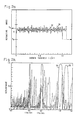
- an optical monitoring signal in this case a single-wavelength reflectance at normal incidence with a monitor wavelength at one-half of the lowest notch wavelength ⁇ 1, dotted line 200, has been juxtaposed to the refractive index profile (solid line 202) subjected to the same errors as in FIG. 2a, but now compensated through corrective actions provided by the algorithm of this invention.
- Both vertical (V at 104) and horizontal (H at 102) index profile corrections are indicated in FIG. 3a and are discussed in further detail below.
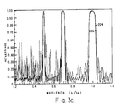
- FIG. 3a shows only the beginning third of the film in order to magnify actions of the algorithm. Random and systematic errors have been taken into account by the algorithm (shown in detail in FIGS. 4a and 4b) which is useful in establishing a highly accurate profile as shown in FIG. 3b and a finely tuned multiple-notch rugate filter, as shown by the reflectance spectrum in FIG. 3c.
- the ideal profile is indicated by the solid line (which is the same as line 32 in FIG.
- FIG. 3c shows the ideal (solid line) 204 and error-compensated (dotted line) 206 reflectance-versus-wavelength spectra. Note the improvement of the error-compensated spectrum 206 of FIG. 3c over the error spectrum 38 of FIG. 2b with the use of the algorithm of the present invention. It should be noted that in FIG. 3a there are more vertical corrections than horizontal corrections since, in this case, the systematic error caused the deposition rate to be too fast.
- the rugate filter is deposited on a uniform substrate according to an algorithm which represents the following considerations in order that the deposition be undertaken in a reliable and controlled fashion.
- the medium is continuously optically monitored to assure that the multiple sinusoidally developing medium profile has measured optical thickness increments that match accurately enough the ideal target optical thickness increments; adjustments are made to the on-going process according to pre-programmed alternative sequences (the algorithm) where the optical thickness signals accurate strictlyly guide a sinusoidal deposition of the optical medium.
- the deposition conditions jump and continue according to where the process conditions should be for this signal rather than where any error may have taken them, or if (2) an optical thickness signal is overdue relative to the current process conditions, then the process conditions hold in an ticipation of the target optical thickness signal. (If no error is present, the deposition process conditions continue according to where they should be.) Consequentially, the subject invention provides for both horizontal and vertical index profile corrective actions. (The terms “horizontal” and “vertical” refer to two perpendicular directions in the index versus thickness plane, as shown in FIG.
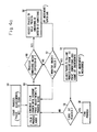
- FIG. 4a shows a flow diagram of the process phase-control algorithm of the present invention.
- An ideal profile of refractive index versus layer thickness is predetermined as a target profile.
- This ideal profile has a multiple-sinusoidal pattern for multiple-notch filters.
- the profile also has predetermined values of optical thickness which can be determined for successive points in time corresponding to points on the ideal target profile.
- target process conditions as a function of time are predetermined which will be effective for forming a layer of optical material guided by the ideal target profile. These process conditions are determined by a series of calibration trials in which variables affecting the chosen process are changed, and the effect on the deposited layer determined.
- Such variables for a chemical deposition process include, but are not limited to, ratios of reactants, concentrations of reactants, flow rate of each reactant, total gas flow rate, pressure, temperature of reactants, temperature of substrate, and rate of deposition.
- reactant as used herein is intended to include materials which interact physically, as well as materials which interact chemically.
- Additional relevant variables for a photochemical process may include the intensity of radiation and distance between the radiation source and the substrate. The process commands for the ideal target profile are then shifted, if necessary for error compensation, during deposition with continual and/or continuous multiple sinusoidal phase adjustments (controlled by the algorithm) relative to the current process conditions and the optical thickness (OT) status.
- n refractive index of optical material
- n average index of refraction over one period in film thickness space (z)
- m total number of rugate transmittance notches
- ⁇ n i i th peak-to-trough index modulation
- ⁇ i i th notch wavelength
- * parameters that can have (unknown) localized random and/or systematic errors, which are compensated for by ⁇ i
- ⁇ i is one component of the multiple-sinusoidal phase-angle adjustment.
- multiple-sinusoidal phase-angle adjustments is used herein to mean the multiple ⁇ i 's required to be commanded simultaneously at each algorithmic decision point to the depositing profile in order to follow accurately the ideal target profile.
- the refractive index can be related to a one-parameter function (e.g., stoichiometric material fraction "y") of the material system, and this one parameter can be controlled as a function of time.
- a one-parameter function e.g., stoichiometric material fraction "y”
- the index is monotonically behaved over a useful range, which means that the inverse relation is also a function or that the system parameter is a function of the index.
- each sinusoid can have a phase correction ⁇ i in n(z; ⁇ i ) of Equation 4 and the target z can be a function of time).
- z z(t) depends on a previously calibrated deposition rate or a deposition rate behavior as a function of time, but if the actual thickness can be determined by an independent thickness monitor (e.g., a calibrated quartz-crystal monitor), then the variable can more usefully be this independently measured thickness, z.
- an independent thickness monitor e.g., a calibrated quartz-crystal monitor
- phase-control algorithm of the present invention can be applied to enhance and sufficiently control such a process by commanding compensation for such errors.
- the process precursors such as silane (SiH4) and nitrous oxide (N2O)
- SiH4 silane
- N2O nitrous oxide
- Equation 9 Because Equation 7 is monotonic in F S , Equation 9 therefore becomes:
- Equation 12 for the algorithmic process commands for achieving the profile design in Equation 4 becomes: where R(t) is the previously calibrated deposition rate or independently measured with a quartz crystal monitor, assuming an average density.
- the process of the present invention is started at box 44.
- the deposition of the optical medium is allowed to start onto the substrate according to a continuous real time control with initial phase adjustments to the process set to zero (process conditions status initially on schedule with no error).
- the process conditions are then guided through Equation (4) above in box 46 (film process guide).
- Inquiry is then made as to whether the current process conditions of deposition of the medium onto the substrate is ahead of the expected optical thickness signal (OT) in box 48. Since the process conditions are initially on schedule at the start 44, flow in the algorithm progresses at least initially to box 52 and then back to 46 since no OT signal will be expected or measured initially. While the process remains (or is assumed to remain) on schedule and no OT is measured ahead of schedule, the algorithm will initially continue in the loop 46-48-52-46.
- the process parameters are commanded to hold at the expected optical thickness process conditions 50.
- This "holding" adjustment occurs when in error the currently depositing film index is too low, or the deposition rate is too small, or the current optical thickness of the profile is too small, and therefore the currently commanded process conditions are ahead of schedule relative to the actually measured optical thickness.
- optical monitoring 52 is conducted. Until the expected optical thickness is actually measured, the algorithm continues in the loop 46-48-50-52-46, which produces commands for continuously changing ⁇ i for a constant, horizontal profile command segment.
- optical monitoring is conducted by reflecting a monitor beam of light off the sample or transmitting a monitor beam of light through the sample, typically at a perpendicular angle of incidence or near perpendicular angle of incidence to provide an optical signal, and determining from this optical signal actual optical thicknesses.
- optical thickness signals are easily provided by intensity minima or maxima in the thusly directed monitor beam of a single wavelength, and these intensity extrema correspond to quarter-waves of optical thickness relative to the monitor beam wavelength. This is referred to in the art as the "turning value" method.
- the algorithm passes the process to box 54 where the phase is fixed at the process conditions for this predetermined optical thickness.
- the loop 46-48-50-52 is terminated into box 54 where the last values for ⁇ i acquired in box 50 are used.
- inquiry is made as to whether the final optical thickness has been reached in box 56. If it has, the process is ended in box 58. If it has not, the film growth process continues with the same phase, at least momentarily, in loop 46-48-52-46 until an affirmative decision in box 48 or 52 is reached.
- Passing through box 54 can alternatively occur without first passing through the 46-48-50-52 sequence. This can happen when the process conditions are exactly on schedule with no error and no phase change necessary.
- the object of the algorithm in FIG. 4a is to maintain accurately the product of the actual average index of refraction ( n ) and the actual component period thicknesses (L i ) so that the Bragg conditions, indicated in Equation (1) above, are maintained component by component, each in their periodically modulated fashions.
- FIG. 3a shows where vertical profile jump corrections are made at 104 to meet the desired Bragg conditions.
- the horizontal profile segments in FIG. 3a correspond with algorithm commands at Box 50 of FIG. 4a where the optical monitoring signal is overdue relative to the current commands of the process conditions, because the current optical thickness rate of deposition is proceeding too slowly, behind schedule.
- the vertical profile jumps 104 of FIG. 3a show the algorithm commands of Box 54 of FIG. 4a where the current optical thickness rate of deposition is proceeding too fast relative to the current commands of the process conditions, so that optical thickness increments are reached too rapidly, ahead of schedule.
- FIG. 4b shows the algorithm with pertinent analytic equations (from Equation (4) herein) to guide the process, where N is the final number of optical thickness signals required to reach the desired notch transmittances or reflectances.
- monitoring can be accomplished with scanning monochromator techniques via the figure-of-merit method which results in film thickness increments that correspond to non quarter-wave optical thicknesses shorter than quarter-wave.
- the present algorithm method of deposition with error-compensation control can be applied to any process which blindly produces a continuously varying refractive index with sinusoidal components.
- the algorithm accomplishes this result by providing corrective process commands to insure sufficient maintenance of the Bragg condition for each component throughout the thin film rugate deposition.
- the process deposition source 158 comprises, for example, two process gases (silane and nitrous oxide) and one purge gas (nitrogen), which are input through separate mass flow controllers (not shown) to a photochemical vapor deposition system (generally indicated at 76) for growth of a rugate film of a selected material, such as SiO x , to form an optical medium.
- the gases are supplied from compressed gas cylinders, and the opening and closing of the valves and the flow of the gases through mass flow controllers in the system are controlled automatically by process computer control 68. Optionally, this control may be performed manually.
- the inflowing silane is used as the silicon source, the nitrous oxide provides a source of oxygen, and both reactants are delivered at flow rates resulting in the predetermined mixture of gases at the deposition substrate or sample 10.
- the gases and optional minute amounts of mercury vapor which acts as a photosensitizer, are then inlet into the system to the reactor chamber 76, where the sample substrate 10 is illuminated with radiation 12 which has a wavelength sufficient to induce the desired photochemical reaction.
- mercury is used as a photosensitizer
- UV radiation of 2537 angstroms from a low-pressure mercury-lamp array is used to induce the reaction to decompose the nitrous oxide and silane compounds and allow the reaction thereof to form a rugate SiO x film, at about 1/1000 of atmospheric pressure.
- Stoichiometry of the film depends on previously calibrated gas flow rates and relative partial pressures of the constituent precursors.
- the exhaust gases are pulled by a process pump (not shown) and pushed to an exhaust manifold for disposal in a safe manner.
- the reactor chamber 76 area may be cross-flushed with laminar air flow to maintain cleanliness during substrate loading or removal.
- FIG. 5 also represents a generalized optical monitoring scheme useful in practicing the present invention required to obtain optical thickness increments.
- Alternative to the simple turning value method more advanced methods including the figure of merit method that involves a wavelength scanning technique, may be used.
- Light is filtered through an optionally scannable monochromator, either at the monitor beam source 166 or at the detector 162, which sets the monitoring probe wavelength(s), ⁇ p .
- the sample 10 is held within the chamber 76, and light from monitor beam source 166 is reflected from mirror 126 onto the sample 10, and then from the sample 10, onto the mirror 128, for output to the external control system beyond the reactor chamber 76.
- witness samples receiving partial filter deposition may be moved into place to monitor the deposition process.
- the reflected monitor beam detector 162 receives the light from the sample 10, and converts the optical input signal from the sample 10 and mirror 128, and electronically processes the optical signal to determine optical thickness increments with the signal processor 164.
- the optical thickness signal processor provides data to the computer control 68 where the algorithm controls the process.
- transmitted beam detector 161 may be used with the system of FIG. 5.
- the computer 68 operates in accordance with the process phase control algorithm shown in FIGS. 4a and 4b.
- FIG. 5 also generically represents the schematic control of any deposition process that is already capable of blindly producing thin films with a continuously varying refractive index in a sinusoidally modulated fashion but susceptible to random and systematic errors.
- thermal evaporation, electron beam evaporation, photochemical vapor deposition, sputter deposition, laser-assisted deposition, etc., and combinations of these techniques can benefit from optical monitoring and algorithm control in accordance with the present invention.
Landscapes
- Chemical & Material Sciences (AREA)
- Physics & Mathematics (AREA)
- General Physics & Mathematics (AREA)
- Optics & Photonics (AREA)
- General Chemical & Material Sciences (AREA)
- Chemical Kinetics & Catalysis (AREA)
- Engineering & Computer Science (AREA)
- Materials Engineering (AREA)
- Mechanical Engineering (AREA)
- Metallurgy (AREA)
- Organic Chemistry (AREA)
- Optical Filters (AREA)
Applications Claiming Priority (2)
| Application Number | Priority Date | Filing Date | Title |
|---|---|---|---|
| US394909 | 1989-08-17 | ||
| US07/394,909 US5009485A (en) | 1989-08-17 | 1989-08-17 | Multiple-notch rugate filters and a controlled method of manufacture thereof |
Publications (3)
| Publication Number | Publication Date |
|---|---|
| EP0416251A2 true EP0416251A2 (de) | 1991-03-13 |
| EP0416251A3 EP0416251A3 (en) | 1991-10-09 |
| EP0416251B1 EP0416251B1 (de) | 1994-06-15 |
Family
ID=23560896
Family Applications (1)
| Application Number | Title | Priority Date | Filing Date |
|---|---|---|---|
| EP90113621A Expired - Lifetime EP0416251B1 (de) | 1989-08-17 | 1990-07-16 | Gesteuertes Verfahren zur Herstellung mehrfacher optischer Rasterfilter |
Country Status (6)
| Country | Link |
|---|---|
| US (1) | US5009485A (de) |
| EP (1) | EP0416251B1 (de) |
| JP (1) | JP2542114B2 (de) |
| KR (1) | KR930007581B1 (de) |
| DE (1) | DE69009909T2 (de) |
| HK (1) | HK107094A (de) |
Cited By (8)
| Publication number | Priority date | Publication date | Assignee | Title |
|---|---|---|---|---|
| EP0562829A1 (de) * | 1992-03-25 | 1993-09-29 | Hughes Aircraft Company | Verbesserte Beschichtungen für Laserdetektor-Etalons |
| EP0562828A1 (de) * | 1992-03-25 | 1993-09-29 | Hughes Aircraft Company | Dispersive Rasterfilter-Beschichtung |
| WO1993019393A1 (en) * | 1992-03-25 | 1993-09-30 | Gec-Marconi Limited | Head-up display system |
| AU646989B2 (en) * | 1992-04-03 | 1994-03-10 | Hughes Aircraft Company | Spatially tunable rugate narrow reflection band filter and applications therefor |
| AU648713B2 (en) * | 1992-04-03 | 1994-04-28 | Raytheon Company | Spatially tunable rugate narrow reflection band filter |
| EP0665577A1 (de) * | 1994-01-28 | 1995-08-02 | Applied Materials, Inc. | Verfahren und Vorrichtung zur Überwachung der Niederschlagsrate von Schichten während physikalischem Dampf-Niederschlag |
| EP1229356A3 (de) * | 2001-01-31 | 2004-01-21 | Planar Systems, Inc. | Verfahren und Vorrichtung zur Herstellung von optischen Filtern |
| CN111687143A (zh) * | 2020-05-20 | 2020-09-22 | 中国民用航空飞行学院 | 一种飞机蒙皮激光分层除漆的实时监测控制方法及系统 |
Families Citing this family (31)
| Publication number | Priority date | Publication date | Assignee | Title |
|---|---|---|---|---|
| US5525156A (en) * | 1989-11-24 | 1996-06-11 | Research Development Corporation | Apparatus for epitaxially growing a chemical compound crystal |
| US5472748A (en) * | 1990-10-15 | 1995-12-05 | The United States Of America As Represented By The United States Department Of Energy | Permanent laser conditioning of thin film optical materials |
| US5181143A (en) * | 1991-10-03 | 1993-01-19 | Rockwell International Corporation | Multiple line rugate filter with index clipping |
| US5258872A (en) * | 1992-10-01 | 1993-11-02 | The United States Of America As Represented By The Secretary Of The Air Force | Optical filter |
| US5354575A (en) * | 1993-04-16 | 1994-10-11 | University Of Maryland | Ellipsometric approach to anti-reflection coatings of semiconductor laser amplifiers |
| DE69422770T2 (de) * | 1993-04-16 | 2000-09-21 | Libbey Owens Ford Co | Verfahren und vorrichtung zum beschichten eines glassubstrates |
| NO941663L (no) * | 1993-05-06 | 1994-11-07 | Hughes Aircraft Co | Rugat filter med undertrykkede harmoniske |
| US5330610A (en) * | 1993-05-28 | 1994-07-19 | Martin Marietta Energy Systems, Inc. | Method of digital epilaxy by externally controlled closed-loop feedback |
| US5549756A (en) * | 1994-02-02 | 1996-08-27 | Applied Materials, Inc. | Optical pyrometer for a thin film deposition system |
| US5928713A (en) * | 1994-09-22 | 1999-07-27 | United States Of America As Represented By The Secretary Of The Air Force | Method for fabricating a gradient refractive index optical filter |
| US5472505A (en) * | 1994-12-19 | 1995-12-05 | Electronics & Telecommunications Research Institute | Apparatus for monitoring films during MOCVD |
| USH1572H (en) * | 1995-01-03 | 1996-08-06 | The United States Of America As Represented By The Secretary Of The Air Force | Wavelength stabilizing laser mirror |
| US5724189A (en) * | 1995-12-15 | 1998-03-03 | Mcdonnell Douglas Corporation | Methods and apparatus for creating an aspheric optical element and the aspheric optical elements formed thereby |
| US5871805A (en) * | 1996-04-08 | 1999-02-16 | Lemelson; Jerome | Computer controlled vapor deposition processes |
| US6162488A (en) * | 1996-05-14 | 2000-12-19 | Boston University | Method for closed loop control of chemical vapor deposition process |
| DE19747597B4 (de) * | 1997-02-12 | 2006-10-05 | Fraunhofer-Gesellschaft zur Förderung der angewandten Forschung e.V. | Vorrichtung zur Darstellung statischer und bewegter Bilder unter Verwendung einer Bildwand, Bildwand sowie Verfahren zur Darstellung und zur Herstellung |
| US6038525A (en) * | 1997-04-30 | 2000-03-14 | Southwest Research Institute | Process control for pulsed laser deposition using raman spectroscopy |
| US6453264B1 (en) | 1997-04-30 | 2002-09-17 | Southwest Research Institute | Surface flaw detection using spatial raman-based imaging |
| US6342265B1 (en) | 1997-08-20 | 2002-01-29 | Triumf | Apparatus and method for in-situ thickness and stoichiometry measurement of thin films |
| US6179039B1 (en) | 1999-03-25 | 2001-01-30 | Visteon Global Technologies, Inc. | Method of reducing distortion in a spray formed rapid tool |
| JP3848571B2 (ja) * | 2001-12-28 | 2006-11-22 | Hoya株式会社 | 薄膜形成方法及び装置 |
| WO2003058699A1 (en) * | 2001-12-31 | 2003-07-17 | Tokyo Electron Limited | Method of fault detection for material process system |
| JP2003342728A (ja) * | 2002-05-24 | 2003-12-03 | Alps Electric Co Ltd | 光学薄膜の成膜装置及び成膜方法 |
| US6956702B2 (en) * | 2003-04-23 | 2005-10-18 | Hewlett-Packard Development Company, L.P. | Projector with spectral filter |
| FR2859485B1 (fr) * | 2003-09-04 | 2006-09-15 | Essilor Int | Procede de realisation d'un traitement anti-reflets sur un substrat optique, substrat optique obtenu par ce procede et dispositif de mise en oeuvre du procede |
| US7901870B1 (en) | 2004-05-12 | 2011-03-08 | Cirrex Systems Llc | Adjusting optical properties of optical thin films |
| US7565084B1 (en) | 2004-09-15 | 2009-07-21 | Wach Michael L | Robustly stabilizing laser systems |
| US7130062B2 (en) * | 2005-01-28 | 2006-10-31 | Raytheon Company | Rapid-response electron-beam deposition system having a controller utilizing leading and trailing deposition indicators |
| GB0516477D0 (en) * | 2005-08-11 | 2005-09-14 | Optical Reference Systems Ltd | Apparatus for measuring semiconductor physical characteristics |
| US7903338B1 (en) | 2006-07-08 | 2011-03-08 | Cirrex Systems Llc | Method and system for managing light at an optical interface |
| EP3208520B1 (de) * | 2014-10-16 | 2023-05-03 | Toppan Printing Co., Ltd. | Quantenpunkt-schutzfolie, quantenpunktfolie damit und hintergrundbeleuchtungseinheit |
Family Cites Families (8)
| Publication number | Priority date | Publication date | Assignee | Title |
|---|---|---|---|---|
| US4332833A (en) * | 1980-02-29 | 1982-06-01 | Bell Telephone Laboratories, Incorporated | Method for optical monitoring in materials fabrication |
| DE3135443A1 (de) * | 1981-09-08 | 1983-03-24 | Leybold-Heraeus GmbH, 5000 Köln | Verfahren und fotometrische anordnung zur dickenmessung und -steuerung optisch wirksamer schichten |
| US4545646A (en) * | 1983-09-02 | 1985-10-08 | Hughes Aircraft Company | Process for forming a graded index optical material and structures formed thereby |
| US4582431A (en) * | 1983-10-11 | 1986-04-15 | Honeywell Inc. | Optical monitor for direct thickness control of transparent films |
| US4676646A (en) * | 1985-10-15 | 1987-06-30 | Energy Conversion Devices, Inc. | Method and apparatus for controlling thickness of a layer of an optical data storage device by measuring an optical property of the layer |
| IL79391A (en) * | 1985-08-14 | 1994-06-24 | Hughes Aircraft Co | Non-spherical patch with a stepped key and a display system that uses it |
| US4837044A (en) * | 1987-01-23 | 1989-06-06 | Itt Research Institute | Rugate optical filter systems |
| US4915476A (en) * | 1988-05-31 | 1990-04-10 | Hughes Aircraft Company | Single-notch rugate filters and a controlled method of manufacture thereof |
-
1989
- 1989-08-17 US US07/394,909 patent/US5009485A/en not_active Expired - Fee Related
-
1990
- 1990-07-16 DE DE69009909T patent/DE69009909T2/de not_active Expired - Fee Related
- 1990-07-16 EP EP90113621A patent/EP0416251B1/de not_active Expired - Lifetime
- 1990-08-15 JP JP2214471A patent/JP2542114B2/ja not_active Expired - Fee Related
- 1990-08-16 KR KR1019900012588A patent/KR930007581B1/ko not_active Expired - Fee Related
-
1994
- 1994-10-06 HK HK107094A patent/HK107094A/en not_active IP Right Cessation
Cited By (12)
| Publication number | Priority date | Publication date | Assignee | Title |
|---|---|---|---|---|
| EP0562829A1 (de) * | 1992-03-25 | 1993-09-29 | Hughes Aircraft Company | Verbesserte Beschichtungen für Laserdetektor-Etalons |
| EP0562828A1 (de) * | 1992-03-25 | 1993-09-29 | Hughes Aircraft Company | Dispersive Rasterfilter-Beschichtung |
| WO1993019393A1 (en) * | 1992-03-25 | 1993-09-30 | Gec-Marconi Limited | Head-up display system |
| GB2265726A (en) * | 1992-03-25 | 1993-10-06 | Marconi Gec Ltd | Head-up display system |
| US5289314A (en) * | 1992-03-25 | 1994-02-22 | Hughes Aircraft Company | Coatings for laser detector etalons |
| AU646989B2 (en) * | 1992-04-03 | 1994-03-10 | Hughes Aircraft Company | Spatially tunable rugate narrow reflection band filter and applications therefor |
| AU648713B2 (en) * | 1992-04-03 | 1994-04-28 | Raytheon Company | Spatially tunable rugate narrow reflection band filter |
| EP0583048B1 (de) * | 1992-04-03 | 1997-07-09 | Hughes Aircraft Company | Raumlich abstimmbarer Smallband-Reflexionsfilter mit kontinuierlich varriierendem Brechungsindex und Anwendung |
| EP0665577A1 (de) * | 1994-01-28 | 1995-08-02 | Applied Materials, Inc. | Verfahren und Vorrichtung zur Überwachung der Niederschlagsrate von Schichten während physikalischem Dampf-Niederschlag |
| US5754297A (en) * | 1994-01-28 | 1998-05-19 | Applied Materials, Inc. | Method and apparatus for monitoring the deposition rate of films during physical vapor deposition |
| EP1229356A3 (de) * | 2001-01-31 | 2004-01-21 | Planar Systems, Inc. | Verfahren und Vorrichtung zur Herstellung von optischen Filtern |
| CN111687143A (zh) * | 2020-05-20 | 2020-09-22 | 中国民用航空飞行学院 | 一种飞机蒙皮激光分层除漆的实时监测控制方法及系统 |
Also Published As
| Publication number | Publication date |
|---|---|
| HK107094A (en) | 1994-10-14 |
| EP0416251B1 (de) | 1994-06-15 |
| DE69009909T2 (de) | 1994-09-22 |
| JPH03149501A (ja) | 1991-06-26 |
| EP0416251A3 (en) | 1991-10-09 |
| JP2542114B2 (ja) | 1996-10-09 |
| US5009485A (en) | 1991-04-23 |
| KR930007581B1 (ko) | 1993-08-13 |
| DE69009909D1 (de) | 1994-07-21 |
| KR910005070A (ko) | 1991-03-29 |
Similar Documents
| Publication | Publication Date | Title |
|---|---|---|
| EP0416251B1 (de) | Gesteuertes Verfahren zur Herstellung mehrfacher optischer Rasterfilter | |
| US4545646A (en) | Process for forming a graded index optical material and structures formed thereby | |
| US4915476A (en) | Single-notch rugate filters and a controlled method of manufacture thereof | |
| US5182670A (en) | Narrow band algan filter | |
| Sullivan et al. | Deposition error compensation for optical multilayer coatings. II. Experimental results—sputtering system | |
| US6160867A (en) | Multi-layer X-ray-reflecting mirrors with reduced internal stress | |
| Sullivan et al. | Deposition error compensation for optical multilayer coatings. I. Theoretical description | |
| US4837044A (en) | Rugate optical filter systems | |
| US20090027776A1 (en) | Method for coating an optical component for a laser arrangement and related optical component | |
| US5000575A (en) | Method of fabricating gradient index optical films | |
| US5160576A (en) | Method of end point detection in a plasma etching process | |
| Stafford et al. | The use of in situ laser interferometry for MOCVD process control | |
| Louis et al. | Multilayer coated reflective optics for Extreme UV lithography | |
| US4335961A (en) | Refractive index measurement of optical thin-film | |
| Bartholomew et al. | Rugate filters by laser flash evaporation of SiOxNy on room temperature polycarbonate | |
| Slaughter et al. | Multilaver Mirrors For 182 | |
| Heitz et al. | Real time control of plasma deposited optical filters by multiwavelength ellipsometry | |
| US20250171888A1 (en) | Method for producing an optical layer system, and an optical layer system produced therewith | |
| Babic et al. | Sputter deposition of precision Si/Si3N4 Bragg reflectors using multitasking interactive processing control | |
| KR100223328B1 (ko) | 고반사율 기판의 노광빛의 반사를 줄이기 위한반사저지박막제조방법 | |
| Babić et al. | In situ characterization of sputtered thin films using a normal incidence laser reflectometer | |
| Wood et al. | Fabrication and characterization of microwave-plasma-assisted chemical vapor deposited dielectric coatings | |
| JPH0881773A (ja) | 高周波スパッタリング装置 | |
| Segner | Plasma impulse chemical vapor deposition | |
| Sheach et al. | Pulsed Plasma Deposition of Optical Filter Structures. |
Legal Events
| Date | Code | Title | Description |
|---|---|---|---|
| PUAI | Public reference made under article 153(3) epc to a published international application that has entered the european phase |
Free format text: ORIGINAL CODE: 0009012 |
|
| 17P | Request for examination filed |
Effective date: 19900716 |
|
| AK | Designated contracting states |
Kind code of ref document: A2 Designated state(s): DE FR GB NL |
|
| PUAL | Search report despatched |
Free format text: ORIGINAL CODE: 0009013 |
|
| AK | Designated contracting states |
Kind code of ref document: A3 Designated state(s): DE FR GB NL |
|
| 17Q | First examination report despatched |
Effective date: 19920903 |
|
| GRAA | (expected) grant |
Free format text: ORIGINAL CODE: 0009210 |
|
| AK | Designated contracting states |
Kind code of ref document: B1 Designated state(s): DE FR GB NL |
|
| REF | Corresponds to: |
Ref document number: 69009909 Country of ref document: DE Date of ref document: 19940721 |
|
| ET | Fr: translation filed | ||
| PGFP | Annual fee paid to national office [announced via postgrant information from national office to epo] |
Ref country code: NL Payment date: 19940731 Year of fee payment: 5 |
|
| PLBE | No opposition filed within time limit |
Free format text: ORIGINAL CODE: 0009261 |
|
| STAA | Information on the status of an ep patent application or granted ep patent |
Free format text: STATUS: NO OPPOSITION FILED WITHIN TIME LIMIT |
|
| 26N | No opposition filed | ||
| PG25 | Lapsed in a contracting state [announced via postgrant information from national office to epo] |
Ref country code: NL Effective date: 19960201 |
|
| NLV4 | Nl: lapsed or anulled due to non-payment of the annual fee |
Effective date: 19960201 |
|
| REG | Reference to a national code |
Ref country code: GB Ref legal event code: 732E |
|
| REG | Reference to a national code |
Ref country code: FR Ref legal event code: TP Ref country code: FR Ref legal event code: CD Ref country code: FR Ref legal event code: CA |
|
| REG | Reference to a national code |
Ref country code: GB Ref legal event code: IF02 |
|
| PGFP | Annual fee paid to national office [announced via postgrant information from national office to epo] |
Ref country code: FR Payment date: 20020610 Year of fee payment: 13 |
|
| PGFP | Annual fee paid to national office [announced via postgrant information from national office to epo] |
Ref country code: GB Payment date: 20020612 Year of fee payment: 13 |
|
| PGFP | Annual fee paid to national office [announced via postgrant information from national office to epo] |
Ref country code: DE Payment date: 20020619 Year of fee payment: 13 |
|
| PG25 | Lapsed in a contracting state [announced via postgrant information from national office to epo] |
Ref country code: GB Free format text: LAPSE BECAUSE OF NON-PAYMENT OF DUE FEES Effective date: 20030716 |
|
| PG25 | Lapsed in a contracting state [announced via postgrant information from national office to epo] |
Ref country code: DE Free format text: LAPSE BECAUSE OF NON-PAYMENT OF DUE FEES Effective date: 20040203 |
|
| GBPC | Gb: european patent ceased through non-payment of renewal fee |
Effective date: 20030716 |
|
| PG25 | Lapsed in a contracting state [announced via postgrant information from national office to epo] |
Ref country code: FR Free format text: LAPSE BECAUSE OF NON-PAYMENT OF DUE FEES Effective date: 20040331 |
|
| REG | Reference to a national code |
Ref country code: FR Ref legal event code: ST |