EP0416582B1 - Leser - Google Patents
Leser Download PDFInfo
- Publication number
- EP0416582B1 EP0416582B1 EP90117088A EP90117088A EP0416582B1 EP 0416582 B1 EP0416582 B1 EP 0416582B1 EP 90117088 A EP90117088 A EP 90117088A EP 90117088 A EP90117088 A EP 90117088A EP 0416582 B1 EP0416582 B1 EP 0416582B1
- Authority
- EP
- European Patent Office
- Prior art keywords
- signal
- card
- sensor unit
- reading device
- recorded
- Prior art date
- Legal status (The legal status is an assumption and is not a legal conclusion. Google has not performed a legal analysis and makes no representation as to the accuracy of the status listed.)
- Expired - Lifetime
Links
Images

Classifications
-
- G—PHYSICS
- G06—COMPUTING OR CALCULATING; COUNTING
- G06K—GRAPHICAL DATA READING; PRESENTATION OF DATA; RECORD CARRIERS; HANDLING RECORD CARRIERS
- G06K7/00—Methods or arrangements for sensing record carriers, e.g. for reading patterns
- G06K7/08—Methods or arrangements for sensing record carriers, e.g. for reading patterns by means detecting the change of an electrostatic or magnetic field, e.g. by detecting change of capacitance between electrodes
- G06K7/082—Methods or arrangements for sensing record carriers, e.g. for reading patterns by means detecting the change of an electrostatic or magnetic field, e.g. by detecting change of capacitance between electrodes using inductive or magnetic sensors
- G06K7/083—Methods or arrangements for sensing record carriers, e.g. for reading patterns by means detecting the change of an electrostatic or magnetic field, e.g. by detecting change of capacitance between electrodes using inductive or magnetic sensors inductive
- G06K7/084—Methods or arrangements for sensing record carriers, e.g. for reading patterns by means detecting the change of an electrostatic or magnetic field, e.g. by detecting change of capacitance between electrodes using inductive or magnetic sensors inductive sensing magnetic material by relative movement detecting flux changes without altering its magnetised state
Definitions
- This invention relates to a reader to read the information magnetically recorded on a card such as a boarding pass.
- a boarding pass having a magnetic stripe has recently been come into use in airports in order to simplify the examination of tickets.
- this magnetic stripe MS is bonded on the back of the boarding pass PS and stores the passenger flight information including a flight number, seat number, passenger name, tag number, etc.
- the flight information is recorded on the magnetic stripe MS through parallel-to-serial conversion and modulation. Some pieces of the information are printed on the surface of the boarding pass.
- Passengers receive boarding passes at the traveler's counter, advance to the boarding gate to the plane, and insert the boarding passes into the reader installed at the boarding gate. The reader reads the flight information from each boarding pass to confirm that the boarding pass is effective.
- the applicant's aim prior art reader against which claim 1 is delimited has four magnetic heads and four demodulation unit, which cooperate to read the flight information regardless of the orientation of the boarding pass inserted into the feeding path.
- the first and second magnetic heads are located under the feeding path and spaced apart in the widthwise direction of the path.
- the third and fourth magnetic heads are arranged above the feeding path and spaced apart in the widthwise direction of the path.
- the magnetic stripe of the boarding pass faces the first magnetic head when the pass is correctly inserted, the second magnetic head when it is inserted with the back to front, the third magnetic head when it is inserted upside down, and the fourth magnetic head when it is inserted the back to front and upside down.
- Each magnetic head detects the signal recorded on the facing magnetic stripe.
- Each demodulation unit demodulates the signal sensed by the corresponding magnetic head and supplies the demodulated signal to the read circuit.
- the read circuit includes a microprocessor, which reads the flight information by extracting a series of digital data from the demodulated signal and converts them into the parallel form.
- each magnetic head is constructed so as to read signals from the four tracks simultaneously, and each demodulation unit includes four independent demodulation ICs for processing the signals read from the four tracks, respectively.
- the reader has 16 demodulation ICs in all, making it difficult to render the reader compact or to reduce the manufacturing cost thereof.
- the magnetic stripe will have more and more tracks because of fractionation of flight information. In this case, the above problem will be all the more serious.
- the read circuit of the reader since the read circuit of the reader must respond to the signal output from any demodulation unit, it is not easy to modify the software for controlling the operation of the microprocessor incorporated in the read circuit. If the number of tracks is increased, the manufacturing cost will greatly increase because it is necessary to modify the software as well as the addition of hardware.
- EP-A3-291342 refers to a card reader being provided with two read-heads. In order to read different cards, or to adjust different orientations of the card, the operator has to select a specific mode.
- the card reader allows reading of the content of the magnetic stripe, even when an operator sets a wrong mode.
- the object of this invention is to provide a reader which can read the information recorded on a card even if the card is incorrectly inserted and which can be manufactured at low cost.
- a reader comprising a feeding path for cards to be inserted in various orientations; a feeding mechanism for advancing the card along the path; a plurality of sensors arranged on the path, each for sensing each signal recorded on the card inserted in a particular orientation; a demodulation unit for demodulating the signal detected by each sensor; a monitor circuit for monitoring the sensors to determine which one of sensors has sensed the recorded signal; a switch circuit for electrically connecting the demodulation unit to the sensor which the monitor circuit determines has sensed the recorded signal; and a read circuit for reading the information of interest by extracting a series of digital data from each demodulation signal output by the demodulation unit and converting the series of digital data into parallel form, in accordance with the particular orientation of the card corresponding to the sensor which the monitor circuit determines has sensed the recorded signal.
- Sensors are arranged on the feeding path for sensing signals recorded on the cards inserted into the path in various orientations. If one of these sensors senses the signal recorded on a card, the monitor determines that the sensor has sensed the signal. The recorded signal is supplied to the demodulation unit through the connecting circuit. The orientation of an inserted card is identified when the monitor circuit confirms that the sensor has sensed the recorded signal. The read circuit extracts a series of digital data from the signal output by the demodulation unit, and converts the series of digital data into the parallel form according to the identified orientation. This operation allows the reader to read the information recorded on the card even if the card is inserted in an incorrect orientation. The recorded signal is sensed by one of the different sensors and supplied to the same demodulation unit.
- the reader does not require a plurality of demodulation units, it can be manufactured at low cost. Moreover, the read circuit can easily be adapted to design modification such as increase in the number of recording tracks on a card, since the circuit is not required to process signals other than the signal output by the signal demodulation unit.
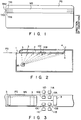
- Fig. 2 shows the internal structure of this reader.
- the reader has an inlet 1 where the existing boarding pass is inserted.
- the boarding pass is supplied from the inlet to a feeding path 2 and then to the outlet 4 along the path 2 by pairs of feeding rollers 3 arranged on the path 2.
- These feeding rollers 3 are driven by a motor M.
- magnetic heads 10A, 10B, 10C, and 10D are installed on the path 2.
- Magnetic head 10A and 10B are located under the path 2, spaced apart in the direction of the widthwise direction thereof.
- Magnetic heads 10C and 10D are arranged above the path 2, spaced apart in the widthwise in the direction. (The magnetic heads 10A and 10D are not shown in Fig.
- the stripe MS on the pass faces any one of the magnetic heads 10A, 10B, 10C, and 10D.
- the magnetic head 10A faces the magnetic stripe MS when the pass PS is correctly inserted.
- the magnetic head 10B faces the stripe MS when the pass PS is inserted with the front side back.
- the magnetic head 10C faces the stripe MS when the pass PS is inserted inside out.
- the magnetic head 10D faces the stripe MS when the pass PS is inserted with the front side back and inside out.
- the magnetic stripe MS comprises four tracks. Each of the magnetic heads 10a to 10D is designed to simultaneously sense the signals recorded in all tracks of the magnetic stripe.
- These magnetic heads 10A to 10D constitute sensor units SR1 to SR4 in combination with the amplifying circuits 11A to 11D, respectively.
- Each of amplifying circuits 11A to 11D comprises four amplifiers AP1 to AP4 for independently amplifying the signals which the corresponding magnetic head has read from four tracks.
- This reader has a demodulation unit 20 for demodulating the four recorded signals sensed by each of the sensor units SR1 to SR4, a monitor circuit MON for monitoring the sensor units SR1 to SR4 to determine which one of sensor units has sensed the recorded signal, a switch circuit 40 for electrically connecting the demodulation unit 20 to the sensor unit which the monitor circuit MON determined has sensed the recorded signal, and a read circuit 30 for reading the flight information by extracting a series of digital data from each signal output by the demodulation unit 20 and for converting the series of digital data into the parallel data in accordance with the orientation of the boarding pass corresponding to the sensor unit which the monitor circuit determines has sensed the signals.
- the switch circuit 40 has four switch groups 41A to 41D corresponding to the sensor units SR1 to SR4. Each switch group has four analog switches SW1 to SW4 connected to receive the signals output from the amplifiers AP1 to AP4 included in the corresponding sensor unit.
- the demodulation unit 20 has four demodulation circuits DM1 to DM4 corresponding to the number of tracks of the magnetic stripe MS.
- the demodulation circuit DM1 is connected to the output terminal of each analog switch SW1 of the switch groups 41A to 41D.
- the demodulation circuit DM2 is connected to the output terminal of each analog switch SW2 of the switch groups 41A to 41D.
- the demodulation circuit DM3 is connected to the output terminal of each analog switch SW3 of the switch groups 41A to 41D.
- the demodulation circuit DM4 is connected to the output terminal of each analog switch SW4 of the switch groups 41A to 41D.
- the demodulation circuits DM1 to DM4 are, for example, the demodulation ICs (Model TCL5010) made by TOHOKU KINZOKU KOGYO Co., Ltd.
- the signals output by amplifiers AP1 to AP4 are waveform-shaped and demodulated by the demodulation circuits DM1 to DM4, respectively, into the demodulation signals RDT1 to RDT4.
- the demodulation circuits DM1 to DM4 extract the clock components from the demodulation signals RDT1 to RDT4, thereby generating the clock signals CLK1 to CLK4 which are phase-adjusted to reproduce the demodulation signals RDT1 through RDT4 as the series of digital data "1" or "0". These demodulation signals RDT1 to RDT4 and the clock signals CLK1 to CLK4 are supplied to the read circuit 30.
- the monitor circuit MON has the amplifiers 50A to 50D and flip-flop circuits 51A to 51D corresponding to the sensor unit SR1 to SR4.
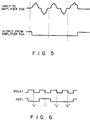
- the amplifiers 50A to 50D amplify, rectify, smooth, and slice the signals output by the amplifiers AP1 of the sensor units SR1 to SR4, thereby generating signals at predetermined levels. These signals are supplied to the clock terminals of the flip-flop circuits 51A to 51D. For example, if the magnetic head 10A senses the recorded signal on the magnetic stripe MS of the boarding pass PS, the signal output by the amplifier AP1 is processed as shown in Fig. 5 and is output from the amplifier 50A.
- Each of the flip-flops 51A to 51D sets the output signal of the Q output terminal at "H” level and that of the Q output terminal at “L” level, at the trailing edge of the signal output by the amplifiers 50A to 50D.
- the Q output terminal of the flip-flop 51A is connected to the control terminal of the analog switches SW1 to SW4 of the switch group 41A, the Q output terminal of the flip-flop 51B to that of the analog switches SW1 to SW4 of the switch group 41B, the Q output terminal of the flip-flop 51C to that of the analog switches SW1 to SW4 of the switch group 41C, and the Q output terminal of the flip-flop 51D to that of the analog switches SW1 to SW4 of the switch group 41D.
- the Q ⁇ output terminals of the flip-flops 51A to 51D are connected to the interrupt terminals INT1 to INT4 of the read circuit 30, respectively.
- the reset terminals of the flip-flops 51A to 51D are connected to the output port OUT2 of the read circuit.
- the flip-flops 51A to 51D respond to the reset signal supplied from the output port OUT2 of the read circuit 30, and set the output signal of the Q output terminal at "L" level and that of the Q ⁇ output terminal at "H” level.
- the switches of groups 41A to 41D are "ON" while the output signals supplied by the Q outputs terminals of the flip-flops 51A to 51D are at "H" level.
- the magnetic stripe MS faces any one of the magnetic heads 10A to 10D, but does not face other magnetic heads. Therefore, only one of the switch groups 41A to 41D can supply the signal output by a corresponding amplifying circuit among those of 11A through 11D to the demodulation unit 20.
- the read circuit 30 comprises a computer including a microprocessor, a ROM, and a RAM.
- the read circuit 30 obtains the flight information by extracting the digital data strings from the demodulation signals RDT1 to RDT4 supplied by the demodulation unit 20 synchronously with the clock signals RCLK1 through RCLK4, and by converting the digital data strings into the parallel form according to the boarding-pass orientation to be clarified by the interrupt terminal set at "L" level among those of INT1 to INT4.
- the magnetic heads 10B and 10D face the magnetic stripe of this boarding pass PS when the boarding pass is inserted with the front side back, and traces the magnetic stripe in the direction opposite to the signal recording direction.
- the read circuit 30 confirms the boarding-pass orientation when the interrupt terminal INT2 or INT4 is set at "L" level, and converts the digital data string into the parallel data items, from the tail to the head, that is, in the opposite direction.
- the read circuit 30 checks the flight information obtained to determine whether or not the boarding pass is effective, and outputs the results from the output port OUT1. Moreover, the read circuit 30 reads the overall flight information from the demodulation signals RDT1 to RDT4 and then generates a reset signal from the output port OUT2.
- the reset signal puts the switch groups 41A to 41D into the non-continuity state, whereby the next boarding pass can be inserted.
- the microprocessor of the read circuit 30 performs the above operation, or the first and second interrupting processes shown in Figs. 7A and 7B. The first interrupting process is performed when the boarding pass is not inserted with the front side back, whereas the second interrupting process is performed when the boarding pass is inserted with the front side back.
- the read circuit 30 also resets the flip-flops 51A through 51D when the power is turned on to bring the switch groups 41A through 41D into the non-continuity state.
- the magnetic stripe of the boarding pass PS faces the magnetic head 10A.
- the stripe is scanned while it is passing through by the magnetic head 10A.
- the magnetic head 10A senses the signals from the tracks TR1 to TR4 of the magnetic stripe MS, the signals recorded on the track TR1 are supplied to the amplifier 50A of the monitor circuit MON from the magnetic head 10A through the amplifier AP1 of the amplifying circuit 11A. Then the signal output from the amplifier 50A falls, and the Q output signal of the flip-flop 51A rises to "H" level.
- the signal records on the tracks TR1 to TR4 are supplied to the demodulation circuits DM1 to DM4 via the analog switches SW1 to SW4, respectively.
- the demodulation circuits DM1 through DM4 demodulate these signals.
- the demodulated signals RDT1 to RDT4, and clock signals RCLK1 to RCLK4 are supplied to the read circuit 30.
- the Q ⁇ output signal of the flip-flop 51A falls to "L" level due to the fall of the signal output by the amplifier 50A, whereby the read circuit 30 executes the process shown in Fig. 7A.
- the read circuit 30 generates a reset signal.
- the reset signal is supplied to the flip-flop 51A to 51D at the final step, and is executed after the boarding pass PS passes through the magnetic head 10A.
- the switch group 41A is brought into the non-continuity state, similarly to the switch groups 41B, 41C, and 41D.
- the magnetic stripe MS of the boarding pass PS faces the magnetic head 10B, and is scanned in the direction opposite to the signal recording direction, while the stripe is passing through the magnetic head 10B.
- the magnetic head 10B senses the recorded signals from the tracks TR1 to TR4 of the magnetic stripe MS
- the signal recorded on the track TR1 is supplied to the amplifier 50B of the monitor circuit MON from the magnetic head 10B through the amplifier AP1 of the amplifying circuit 11B. Then, the signal output from the amplifier 50B falls, and the Q output signal of the flip-flop 51B rises to "H" level.
- the signals recorded on tracks TR1 to TR4 are supplied to the demodulation circuits DM1 to DM4 through the analog switches SW1 to SW4, respectively.
- the demodulation circuits DM1 to DM4 demodulate these signals.
- the demodulated signals RDT1 to RDT4, and clock signals RCLK1 to RCLK4 are supplied to the read circuit 30.
- the Q ⁇ output signal of the flip-flop 51B falls to "L" level due to the fall of the signal output by the amplifier 50B, whereby the read circuit 30 executes the process shown in Fig. 7B.
- the read circuit 30 generates a reset signal, which is input to the flip-flops 51A to 51D at the final step, to be executed after the boarding pass PS passes through the magnetic head 10B.
- the switch group 41B is brought into the non-continuity state similarly to the switch groups 41A, 41C, and 41D.
- the boarding pass PS is inserted into the inlet 1 upside down.
- the magnetic stripe of the boarding pass PS faces the magnetic head 10C, and is scanned in the signal recording direction while the stripe is passing through the magnetic head 10C.
- the signal recorded on the track TR1 is supplied to the amplifier 50C of the monitor circuit MON through the amplifier AP1 of the amplifying circuit 11C from the magnetic head 10C. Then the signal output by the amplifier 50C falls, and the Q output signal of the flip-flop 51C rises to "H" level.
- the signals recorded on tracks TR1 to TR4 are supplied to the demodulation circuits DM1 to DM4 through the analog switches SW1 to SW4, respectively.
- the demodulation circuits DM1 to DM4 demodulate these signals.
- the demodulated signals RDT1 to RDT4, and clock signals RCLK1 to RCLK4 are supplied to the read circuit 30.
- the Q ⁇ output signal of the flip-flop 51C falls to "L" level due to the fall of the signal output by the amplifier 50B, whereby the read circuit 30 executes the processing shown in Fig. 7A.
- the read circuit 30 generates a reset signal, which is supplied to the flip-flops 51A to 51D at the final step to be executed after the boarding pass PS passes through the magnetic head 10C.
- the switch group 41C is brought into the non-continuity state, similarly to the switch groups 41A, 41B, and 41D.
- the boarding pass PS is inserted into the inlet 1 back to front and upside down.
- the magnetic stripe of the boarding pass PS faces the magnetic head 10D, and is scanned in the direction opposite to the signal recording direction while the stripe is passing through the magnetic head 10D.
- the signal recorded on the track TR1 is supplied to the amplifier 50D of the monitor circuit MON through the amplifier AP1 of the amplifying circuit 11D from the magnetic head 10D. Then, the signal output by the amplifier 50D falls, and the Q output signal of the flip-flop 51D rises to "H" level.
- the read circuit 30 generates the reset signal, which is supplied to the flip-flops 51A through 51D at the final step to be executed after the boarding pass PS passes through the magnetic head 10D.
- the switch group 41D is brought into the non-continuity state, similarly to the switch groups 41A, 41B, and 41C.
- the sensor units SR1 to SR4 are arranged on the path 2 so as to detect boarding passes inserted onto the path 2 in various orientations. If one of the sensor units SR1 to SR4 (e.g., SR1) senses the signals recorded on the boarding pass, the monitor circuit MON determines this fact, and the signals are supplied to the demodulation unit 20 through the switch circuit 40. The orientation of the boarding pass inserted is determined when the monitor circuit MON confirms that the sensor unit SR1 has sensed the recorded signals.
- the read circuit 30 extracts digital data strings from the signals RDT1 to RDT4 output from the demodulation unit 20 and converts these data strings into the parallel data, in accordance with the orientation.
- the flight information recorded on the boarding pass in the form of signals, can be read even if the pass is inserted in an incorrect orientation.
- Each recorded signal is sensed by one of sensor units and supplied to the same demodulation unit 20. Since the reader does not require a plurality of demodulation units, it can be manufactured at low cost.
- the read circuit 30 can easily be adapted to design modification such as increase of the number of recording tracks of a boarding pass, since the circuit is not required to process signals other than the output signal of the single demodulation unit 20.
Landscapes
- Engineering & Computer Science (AREA)
- Artificial Intelligence (AREA)
- Computer Vision & Pattern Recognition (AREA)
- Physics & Mathematics (AREA)
- General Physics & Mathematics (AREA)
- Theoretical Computer Science (AREA)
- Devices For Checking Fares Or Tickets At Control Points (AREA)
- Digital Magnetic Recording (AREA)
- Recording Or Reproducing By Magnetic Means (AREA)
Claims (8)
- Leseeinrichtung zum Lesen eines auf einer Karte aufgezeichneten Informationssignals, ungeachtet der Ausrichtung der Karte relativ zur Leseeinrichtung, mit:einem Zuführweg (2) zur Aufnahme einer Karte, welche in einer von verschiedenen Ausrichtungen zuführbar ist,einem Mechanismus (3, M) zum Weiterführen der Karte entlang dem Zuführweg; undmehreren Sensoreinheiten (SR1 bis SR4) zum Erfassen eines auf der Karte aufgezeichneten Signals, wobei die Sensoreinheiten auf dem Zuführweg (2) derart angeordnet sind, daß eine der Sensoreinheiten (SR1 bis SR4) das auf der Karte aufgezeichnete Signal erfaßt, wenn die Karte mit einer speziellen jeweiligen Ausrichtung von verschiedenen möglichen Ausrichtungen eingeführt ist;gekennzeichnet durcheine Überwachungseinrichtung (MON) zum Überwachen aller Sensoreinheiten (SR1 bis SR4), um zu Bestimmen, welche der Sensoreinheiten (SR1 bis SR4) das Signal erfaßt hat;eine einzige Demodulationseinheit (20) zum Demodulieren eines durch die Sensoreinheit (SR1 bis SR4) erfaßten Signals;eine Verbindungseinrichtung (40) zum elektrischen Verbinden der einzigen Demodulationseinheit (20) mit der Sensoreinheit (SR1 bis SR4), welche gemäß der Überwachungseinrichtung (MON) das Signal erfaßt hat, um das durch die Sensoreinheit (SR1 bis SR4) erfaßte Signal zu demodulieren; undeine Leseeinrichtung (30) zum Lesen der interessierenden Information, indem eine Reihe von digitalen Daten aus dem Signalausgang durch die Demodulationseinheit (20) gewonnen wird, und zum Umwandeln der Reihe von digitalen Daten in Parallelform entsprechend der speziellen Ausrichtung der Karte, welche der Sensoreinheit (SR1 bis SR4) zugeordnet wurde, welche gemäß der Überwachungseinrichtung (MON) das aufgezeichnete Signal erfaßt hat.
- Leseeinrichtung nach Anspruch 1, dadurch gekennzeichnet, daß die Überwachungseinrichtung mehrere Erfassungsschaltungen (50A bis 50D, 51A bis 51D) aufweist, welche jeweils mit den Sensoreinheiten (SR1 bis SR4) verbunden sind, wobei jede Erfassungsschaltung kontinuierlich ein Kartenerfassungssignal in Abhängigkeit von dem von einer entsprechenden Sensoreinheit (SR1 bis SR4) zugeführten Signal erzeugt, wenn die entsprechende Sensoreinheit (SR1 bis SR4) das aufgezeichnete Signal erfaßt hat.
- Leseeinrichtung nach Anspruch 2, dadurch gekennzeichnet, daß die Verbindungseinrichtung mehrere Schaltkreise (41A bis 41D) aufweist, von denen jeder mit einer entsprechenden Sensoreinheit (SR1 bis SR4) und mit der einzigen Demodulationseinheit (20) verbunden ist und von denen jeder eine Zuführung des Ausgangssignals der entsprechenden Sensoreinheit (SR1 bis SR4) zu der einzigen Demodulationseinheit (20) in Abhängigkeit von dem von der entsprechenden Erfassungsschaltung (50A bis 50D, 51A bis 51D) erzeugten Kartenerfassungssignal ermöglicht.
- Leseeinrichtung nach Anspruch 3, dadurch gekennzeichnet, daß die Leseeinrichtung (30) mit den Erfassungsschaltungen (50A bis 50D, 51A bis 51D) verbunden ist, um zu Bestimmen, welche der Erfassungsschaltungen (50A bis 50D, 51A bis 51D) das Kartenerfassungssignal erzeugt hat.
- Leseeinrichtung nach Anspruch 4, dadurch gekennzeichnet, daß die Leseeinrichtung eine Einrichtung zum Initialisieren der Erfassungsschaltungen (50A bis 50D, 51A bis 51D), nachdem die interessierende Information gelesen wurde, aufweist.
- Leseeinrichtung nach Anspruch 5, dadurch gekennzeichnet, daß jede Sensoreinheit einen mehrspurigen Magnetkopf (10A bis 10D) und mehrere Verstärker (AP1 bis AP4) aufweist, welche mit dem mehrspurigen Magnetkopf (10A bis 10D) verbunden sind, wobei die einzige Demodulationseinheit mehrere Demodulatoren (DM1 bis DM4) umfaßt und jeder Schaltkreise mehrere Schalter (SW1 bis SW4) aufweist, welche jeweils mit den Verstärkern (AP1 bis AP4) einer entsprechenden Sensoreinheit (SR1 bis SR4) und mit den Demodulatoren (DM1 bis DM4) der einzigen Demodulationseinheit (20) verbunden sind.
- Leseeinrichtung nach Anspruch 6, dadurch gekennzeichnet, daß jede Erfassungsschaltung (50A bis 50D, 51A bis 51D) verbunden ist, um das Ausgangssignal eines Verstärkers (AP1 bis AP4) einer entsprechenden Sensoreinheit (SR1 bis SR4) zu empfangen.
- Leseeinrichtung nach Anspruch 7, dadurch gekennzeichnet, daß jede Erfassungsschaltung einen Verstärker (50A bis 50D) und ein Flip-Flop (51A bis 51D) umfaßt.
Applications Claiming Priority (2)
| Application Number | Priority Date | Filing Date | Title |
|---|---|---|---|
| JP232423/89 | 1989-09-07 | ||
| JP1232423A JPH0827890B2 (ja) | 1989-09-07 | 1989-09-07 | ボーディングパスの読取装置 |
Publications (3)
| Publication Number | Publication Date |
|---|---|
| EP0416582A2 EP0416582A2 (de) | 1991-03-13 |
| EP0416582A3 EP0416582A3 (en) | 1991-05-02 |
| EP0416582B1 true EP0416582B1 (de) | 1996-01-03 |
Family
ID=16939033
Family Applications (1)
| Application Number | Title | Priority Date | Filing Date |
|---|---|---|---|
| EP90117088A Expired - Lifetime EP0416582B1 (de) | 1989-09-07 | 1990-09-05 | Leser |
Country Status (4)
| Country | Link |
|---|---|
| US (1) | US5291005A (de) |
| EP (1) | EP0416582B1 (de) |
| JP (1) | JPH0827890B2 (de) |
| DE (1) | DE69024568T2 (de) |
Families Citing this family (7)
| Publication number | Priority date | Publication date | Assignee | Title |
|---|---|---|---|---|
| JP2962627B2 (ja) * | 1993-01-20 | 1999-10-12 | 沖電気工業株式会社 | 磁気データ読取装置 |
| US5446271A (en) * | 1993-08-06 | 1995-08-29 | Spectra-Physics Scanning Systems, Inc. | Omnidirectional scanning method and apparatus |
| JP2902272B2 (ja) * | 1993-08-27 | 1999-06-07 | 株式会社三協精機製作所 | 磁気カードリーダ |
| JP3157362B2 (ja) * | 1993-09-03 | 2001-04-16 | 株式会社東芝 | 半導体装置 |
| US5770847A (en) * | 1994-12-23 | 1998-06-23 | Spectra-Physics Scanning Systems, Inc. | Bar code reader with multi-focus lens |
| US5814803A (en) * | 1994-12-23 | 1998-09-29 | Spectra-Physics Scanning Systems, Inc. | Image reader with multi-focus lens |
| US20060111973A1 (en) * | 2004-11-23 | 2006-05-25 | First Data Corporation | Stored value mileage card systems and methods of use |
Family Cites Families (6)
| Publication number | Priority date | Publication date | Assignee | Title |
|---|---|---|---|---|
| GB1207334A (en) * | 1966-10-04 | 1970-09-30 | Omron Tateisi Electronics Co | A card reading system |
| JPS59180626A (ja) * | 1983-03-30 | 1984-10-13 | Fujitsu Kiden Ltd | 磁気カ−ドデ−タ読取制御方式 |
| JPS60132287A (ja) * | 1983-12-20 | 1985-07-15 | Fujitsu Ltd | 磁気カ−ドの誤插入防止方式 |
| JPS62189588A (ja) * | 1986-02-15 | 1987-08-19 | Nec Corp | 磁気カ−ド読取装置 |
| US4918298A (en) * | 1986-12-01 | 1990-04-17 | Omron Tateisi Electronics Co. | Checkin gate apparatus |
| JPH0786897B2 (ja) * | 1987-05-15 | 1995-09-20 | シャープ株式会社 | カ−ド状体の読取り装置 |
-
1989
- 1989-09-07 JP JP1232423A patent/JPH0827890B2/ja not_active Expired - Fee Related
-
1990
- 1990-09-04 US US07/577,460 patent/US5291005A/en not_active Expired - Fee Related
- 1990-09-05 EP EP90117088A patent/EP0416582B1/de not_active Expired - Lifetime
- 1990-09-05 DE DE69024568T patent/DE69024568T2/de not_active Expired - Fee Related
Also Published As
| Publication number | Publication date |
|---|---|
| EP0416582A2 (de) | 1991-03-13 |
| JPH0395704A (ja) | 1991-04-22 |
| DE69024568T2 (de) | 1996-05-15 |
| EP0416582A3 (en) | 1991-05-02 |
| US5291005A (en) | 1994-03-01 |
| JPH0827890B2 (ja) | 1996-03-21 |
| DE69024568D1 (de) | 1996-02-15 |
Similar Documents
| Publication | Publication Date | Title |
|---|---|---|
| US4041279A (en) | Data reading device | |
| US4863196A (en) | Certification identifying medium | |
| US4356473A (en) | Monetary document profile location and predetermined selected path apparatus | |
| EP0317229A2 (de) | Prüfungsverfahren und -system | |
| EP0134110A2 (de) | Lese- und Schreibvorrichtung für Identifizierungskarten | |
| EP0416582B1 (de) | Leser | |
| EP0082928B1 (de) | Erkennungsgerät für Zeichen mit magnetischer Tinte | |
| GB2308213A (en) | Integrated circuit (IC) card reader | |
| CY1575A (en) | Iron complexes | |
| JPH10511784A (ja) | セキュリティ・スレッド検出装置 | |
| EP0049337B1 (de) | Vorrichtung mit maschinell ablesbarem Datenträgerstreifen | |
| JPH01120691A (ja) | Icカード識別方式 | |
| JPS5530739A (en) | Automatic transaction unit | |
| JPS6170690A (ja) | 紙葉類鑑別方法 | |
| KR930003414B1 (ko) | 자기카드의 검출 제어방법 | |
| JPH0312060A (ja) | 異種磁気カード共用型リードライタ | |
| JP4042320B2 (ja) | 磁気パターンの認識方法、情報記録媒体、磁気パターン認識装置及び複合処理装置 | |
| JP2750766B2 (ja) | 磁気記録カードのパンチ穴検出方式 | |
| JPS6194271A (ja) | 磁気カ−ド | |
| JPH07169179A (ja) | 磁気カードリーダライタシステム | |
| JP2521544Y2 (ja) | 磁気カード読取装置 | |
| JP2003162690A (ja) | カードリーダー・ライター | |
| JPS6055485A (ja) | タイムカ−ドリ−ダ | |
| EP0969402A3 (de) | System und Verfahren zur Verarbeitung einer Identifikationskarte | |
| JPS6220096A (ja) | 自動販売機 |
Legal Events
| Date | Code | Title | Description |
|---|---|---|---|
| PUAI | Public reference made under article 153(3) epc to a published international application that has entered the european phase |
Free format text: ORIGINAL CODE: 0009012 |
|
| 17P | Request for examination filed |
Effective date: 19900905 |
|
| AK | Designated contracting states |
Kind code of ref document: A2 Designated state(s): DE FR GB SE |
|
| PUAL | Search report despatched |
Free format text: ORIGINAL CODE: 0009013 |
|
| AK | Designated contracting states |
Kind code of ref document: A3 Designated state(s): DE FR GB SE |
|
| 17Q | First examination report despatched |
Effective date: 19940103 |
|
| GRAA | (expected) grant |
Free format text: ORIGINAL CODE: 0009210 |
|
| AK | Designated contracting states |
Kind code of ref document: B1 Designated state(s): DE FR GB SE |
|
| PG25 | Lapsed in a contracting state [announced via postgrant information from national office to epo] |
Ref country code: FR Effective date: 19960103 |
|
| RAP1 | Party data changed (applicant data changed or rights of an application transferred) |
Owner name: KABUSHIKI KAISHA TEC |
|
| REF | Corresponds to: |
Ref document number: 69024568 Country of ref document: DE Date of ref document: 19960215 |
|
| PG25 | Lapsed in a contracting state [announced via postgrant information from national office to epo] |
Ref country code: SE Effective date: 19960403 |
|
| EN | Fr: translation not filed | ||
| PLBE | No opposition filed within time limit |
Free format text: ORIGINAL CODE: 0009261 |
|
| STAA | Information on the status of an ep patent application or granted ep patent |
Free format text: STATUS: NO OPPOSITION FILED WITHIN TIME LIMIT |
|
| 26N | No opposition filed | ||
| PGFP | Annual fee paid to national office [announced via postgrant information from national office to epo] |
Ref country code: DE Payment date: 20010828 Year of fee payment: 12 |
|
| PGFP | Annual fee paid to national office [announced via postgrant information from national office to epo] |
Ref country code: GB Payment date: 20010905 Year of fee payment: 12 |
|
| REG | Reference to a national code |
Ref country code: GB Ref legal event code: IF02 |
|
| PG25 | Lapsed in a contracting state [announced via postgrant information from national office to epo] |
Ref country code: GB Free format text: LAPSE BECAUSE OF NON-PAYMENT OF DUE FEES Effective date: 20020905 |
|
| PG25 | Lapsed in a contracting state [announced via postgrant information from national office to epo] |
Ref country code: DE Free format text: LAPSE BECAUSE OF NON-PAYMENT OF DUE FEES Effective date: 20030401 |
|
| GBPC | Gb: european patent ceased through non-payment of renewal fee |
Effective date: 20020905 |