EP0416809A2 - Methode zum Ätzen von Mustern mit reduzierten Grössen für integrierte Schaltungen - Google Patents
Methode zum Ätzen von Mustern mit reduzierten Grössen für integrierte Schaltungen Download PDFInfo
- Publication number
- EP0416809A2 EP0416809A2 EP90309482A EP90309482A EP0416809A2 EP 0416809 A2 EP0416809 A2 EP 0416809A2 EP 90309482 A EP90309482 A EP 90309482A EP 90309482 A EP90309482 A EP 90309482A EP 0416809 A2 EP0416809 A2 EP 0416809A2
- Authority
- EP
- European Patent Office
- Prior art keywords
- pattern transfer
- transfer material
- opening
- material layer
- layer
- Prior art date
- Legal status (The legal status is an assumption and is not a legal conclusion. Google has not performed a legal analysis and makes no representation as to the accuracy of the status listed.)
- Withdrawn
Links
Images


Classifications
-
- H—ELECTRICITY
- H10—SEMICONDUCTOR DEVICES; ELECTRIC SOLID-STATE DEVICES NOT OTHERWISE PROVIDED FOR
- H10P—GENERIC PROCESSES OR APPARATUS FOR THE MANUFACTURE OR TREATMENT OF DEVICES COVERED BY CLASS H10
- H10P76/00—Manufacture or treatment of masks on semiconductor bodies, e.g. by lithography or photolithography
- H10P76/40—Manufacture or treatment of masks on semiconductor bodies, e.g. by lithography or photolithography of masks comprising inorganic materials
- H10P76/408—Manufacture or treatment of masks on semiconductor bodies, e.g. by lithography or photolithography of masks comprising inorganic materials characterised by their sizes, orientations, dispositions, behaviours or shapes
- H10P76/4088—Processes for improving the resolution of the masks
-
- H—ELECTRICITY
- H10—SEMICONDUCTOR DEVICES; ELECTRIC SOLID-STATE DEVICES NOT OTHERWISE PROVIDED FOR
- H10P—GENERIC PROCESSES OR APPARATUS FOR THE MANUFACTURE OR TREATMENT OF DEVICES COVERED BY CLASS H10
- H10P50/00—Etching of wafers, substrates or parts of devices
- H10P50/69—Etching of wafers, substrates or parts of devices using masks for semiconductor materials
- H10P50/691—Etching of wafers, substrates or parts of devices using masks for semiconductor materials for Group V materials or Group III-V materials
- H10P50/693—Etching of wafers, substrates or parts of devices using masks for semiconductor materials for Group V materials or Group III-V materials characterised by their size, orientation, disposition, behaviour or shape, in horizontal or vertical plane
- H10P50/696—Process specially adapted to improve the resolution of the mask
-
- H—ELECTRICITY
- H10—SEMICONDUCTOR DEVICES; ELECTRIC SOLID-STATE DEVICES NOT OTHERWISE PROVIDED FOR
- H10P—GENERIC PROCESSES OR APPARATUS FOR THE MANUFACTURE OR TREATMENT OF DEVICES COVERED BY CLASS H10
- H10P50/00—Etching of wafers, substrates or parts of devices
- H10P50/73—Etching of wafers, substrates or parts of devices using masks for insulating materials
-
- H—ELECTRICITY
- H10—SEMICONDUCTOR DEVICES; ELECTRIC SOLID-STATE DEVICES NOT OTHERWISE PROVIDED FOR
- H10P—GENERIC PROCESSES OR APPARATUS FOR THE MANUFACTURE OR TREATMENT OF DEVICES COVERED BY CLASS H10
- H10P76/00—Manufacture or treatment of masks on semiconductor bodies, e.g. by lithography or photolithography
- H10P76/40—Manufacture or treatment of masks on semiconductor bodies, e.g. by lithography or photolithography of masks comprising inorganic materials
-
- H—ELECTRICITY
- H10—SEMICONDUCTOR DEVICES; ELECTRIC SOLID-STATE DEVICES NOT OTHERWISE PROVIDED FOR
- H10W—GENERIC PACKAGES, INTERCONNECTIONS, CONNECTORS OR OTHER CONSTRUCTIONAL DETAILS OF DEVICES COVERED BY CLASS H10
- H10W20/00—Interconnections in chips, wafers or substrates
- H10W20/01—Manufacture or treatment
- H10W20/071—Manufacture or treatment of dielectric parts thereof
- H10W20/081—Manufacture or treatment of dielectric parts thereof by forming openings in the dielectric parts
- H10W20/082—Manufacture or treatment of dielectric parts thereof by forming openings in the dielectric parts the openings being tapered via holes
-
- H—ELECTRICITY
- H10—SEMICONDUCTOR DEVICES; ELECTRIC SOLID-STATE DEVICES NOT OTHERWISE PROVIDED FOR
- H10W—GENERIC PACKAGES, INTERCONNECTIONS, CONNECTORS OR OTHER CONSTRUCTIONAL DETAILS OF DEVICES COVERED BY CLASS H10
- H10W20/00—Interconnections in chips, wafers or substrates
- H10W20/01—Manufacture or treatment
- H10W20/071—Manufacture or treatment of dielectric parts thereof
- H10W20/081—Manufacture or treatment of dielectric parts thereof by forming openings in the dielectric parts
- H10W20/089—Manufacture or treatment of dielectric parts thereof by forming openings in the dielectric parts using processes for implementing desired shapes or dispositions of the openings, e.g. double patterning
Definitions
- This invention relates to methods for the manufacture of semiconductor integrated circuits and more particularly to methods for controlled etching of various layers employed in semiconductor fabrication.
- Typical integrated circuit manufacturing processes often involve the creation of openings in various materials by selective etching.
- openings termed “trenches” are often made in a substrate such as silicon to provide isolation between individual devices or to provide capacitive charge storage.
- Other openings termed “vias” or “windows” or “contact holes” are often made in dielectric layers to facilitate connection between two layers of metallization or between a metallization layer and an active region of a transistor.
- these openings are created by depositing a photoresist upon the material in which the opening is to be made. Portions of the photoresist are exposed to light.
- the exposed or the unexposed portion of the photoresist is washed away (depending upon whether a positive or negative photoresist is employed) leaving selected portions of the underlying material exposed. With the remaining resist serving as a mask, the exposed portions of the underlying material are etched through to create openings.
- the openings may be subsequently filled with appropriate materials. For example, if the opening is a trench, the trench may be filled with insulative material to facilitate inter-device isolation. If the trench is to be used for capacitance storage, it may be lined with one or more layers of conductive material. Vias or windows may be subsequently filled with a conductive material, for example a metal, thus providing a conductive link between two layers of metallization or between a source/drain and an overlying metallization.
- Zero delta processes Processes which faithfully reproduce the patterned resist in the underlying material (with vertical walls) may be termed "zero delta" processes because there is no difference in feature width between the resist and the underlying material.
- zero delta processes are subsequently modified to create features with sloping walls. Examples of zero delta processes modified to create sloping walls are the formation of sloped vias (for improved metal step coverage) and the information of metal runners with sloped walls (for improved dielectric coverage).
- the smallest between-feature width as well as the smallest opening in zero delta processes (even with sloped walls) is generally limited by lithography.
- the present invention is a non-zero delta process which permits the formation of openings with dimensions smaller than those achievable by whatever lithographic processes may be available.
- a material layer (termed a "pattern transfer material") is deposited between the underlying material into which an opening is to be etched and the overlying photoresist.
- the pattern transfer material is sandwiched between the material-to-be-etched and the photoresist.
- the photoresist is patterned by conventional techniques to define the opening.
- the pattern transfer material is then etched with a process which creates an inward sloping profile.
- the sloping profile serves to define an opening at the interface between the pattern transfer material and the underlying substrate.
- the dimensions of the opening defined in the pattern transfer material are smaller than the corresponding opening in the photoresist.
- the pattern transfer material is next used as a mask to etch the underlying material, thus creating openings which have dimensions smaller than achievable by lithography in the photoresist.
- the openings may be utilized in a variety of ways, for example, as windows or vias, as trenches, or even as patterns for oxide growth.
- reference numeral 11 designates a substrate which may consist essentially of, for example, silicon, epitaxial silicon, gallium arsenide, or another suitable material.
- Reference numerals 13 and 15 designate a gate oxide and an overlying conductive material which, for example, may be polysilicon.
- the combination of elements 13 and 15 is often termed the "gate stack".
- the gate stack is designed by reference numeral 25.
- the invention is applicable to a variety of devices with more complex gate structures, including gates with silicide on top. A simple gate stack is shown here for convenience.
- Reference numerals 17 and 19 designate a source and drain respectively.
- Reference numeral 21 designates a field oxide which serves to provide inter-device isolation. The invention is applicable to integrated circuit structures which use other means of inter-device isolation.
- Reference numeral 23 designates a gate runner which may connect two transistors.
- the basic transistor structure described above is a typical MOS transistor. However, the invention may be applied to a wide variety of transistor types, including bipolar transistors. For convenience, application of the invention to MOS transistors alone will be described.
- Dielectric 27 is formed over the previously described transistor structure. Dielectric 27 is often an oxide of silicon formed by chemical vapor deposition. It is assumed that it is desired to open windows or vias through dielectric 27 so that a conductive material, typically, aluminum or tungsten or polysilicon may be deposited in the windows or vias. The conductive material will be subsequently patterned to form conductive interconnections between various components.
- a conductive material typically, aluminum or tungsten or polysilicon
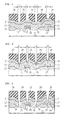
- Photoresist 29 overlies dielectric 27. It is assumed that the smallest feature width that can be lithographically printed in photoresist 29 is D. Figure 1 illustrates patterned openings in photoresist, each with width D. A patterned opening is illustrated in Fig. 1 in photoresist 29 above each source 17, drain 19, gate 25 and runner 23. Of course, it is not necessary for the practice of the invention that all of the above-illustrated openings be transferred to the underlying dielectric 27.
- the present invention provides a method of creating openings such as windows (also termed “contact holes”) in dielectric 27 which are smaller than the smallest achievable lithographic width D.
- the reduction in width is accomplished be depositing layer 31 (termed “pattern transfer material”) on top of dielectric 27 before photoresist 29 is deposited and patterned.
- Fig. 1 illustrates layer 31 sandwiched between dielectric 27 and patterned photoresist 29.
- Suitable candidate materials for pattern transfer material 27 are: polysilicon, tantalum silicide. aluminum, titanium, titanium-tungsten, and tungsten. Whatever material is employed for the pattern transfer material 31, it must be a material which can be etched to produce an inward sloping profile. (Of course, an undercut profile would not produce the desired result).
- Fig. 2 illustrates the results obtained when pattern transfer material 31 is etched, using patterned photoresist 29 as a mask, to produce a sloping profile.
- Each of the walls 32 produced by the etch process slopes inward. It should be noted that the width of the window at the bottom of the pattern transfer material 31 has a width with dimension T which is smaller than the smallest lithographically achievable dimension, D, mentioned above. Dimension T is smaller than dimension D, because the walls 32 slope inward. Examples of etch processes which will produce the desired sloping walls 32 will be discussed in forthcoming paragraphs.
- pattern transfer material 31 is used as a mask for the next etch step.
- dielectric 27 is etched through pattern transfer material 31.
- Each of the windows vias created in dielectric 27 will have a width T similar to the width of the windows or vias created in pattern transfer material 31.
- the inventive process has created windows 34 through dielectric 27 to source 17, drain 19, gate 25 or runner 23 which have a width T, smaller than the smallest achievable lithographic dimension D.
- the process described above is not a zero-delta process since the resulting etched width T is smaller than the lithographic width D.
- the delta of the inventive process may be controlled by the amount of slope created on walls 32 and by the thickness of pattern transfer material 31.
- windows or vias 34 are created, standard processing steps may be performed, including removal of the pattern transfer material 31 (if desired) and creation of the appropriate metallization scheme.
- etching techniques that produce sloped walls in various materials. Generally, it is believed that such etching techniques accomplish their result by the formation of a polymeric sidewall which tends to protect the side of the material under etch, creating a sloped side. However, other mechanisms may be responsible for creation of sloped sides under various circumstances (such as deposition of reaction products or feed gas species by control of the substrate temperature).
- a suitable etch process which may be employed when the pattern transfer material is aluminum is contained in copending application entitled “ Method and Apparatus for Tapered Etching” filed on June 30, 1988, designated “Bredbenner-1" and assigned to the assignee of the present application, and incorporated herein by reference.
- TEOS tetraethylorthosilane
- the photoresist was patterned using a standard reticle for formation of 1.0 ⁇ m windows or elongated trenches. Then the pattern transfer material was patterned with trichlorofluoromethane at a flow of 60 sccm and at 10 ⁇ m pressure. It has been established that the addition of oxygen to this etch process reduces protective sidewall growth while increased bias or power in the etch increases sidewall growth (and therefore increases the amount of slope obtained in the pattern transfer material layer). Consequently, a high bias voltage (in the absence of oxygen) of approximately -500V was employed to etch the polysilicon in a hexode reactor.
- the underlying oxide was etched using trifluoromethane and oxygen.
- the resulting reductions in widths of the vias or trenches in the oxide were 0.5 ⁇ m for the 4000 ⁇ polysilicon material and 0.24 ⁇ m for the 2500 ⁇ tantalum silicide.
- the amount of width reduction depended upon the thickness of the pattern transfer material, a thicker pattern transfer material producing a greater width reduction.
- a process whose anisotropy is controlled by a sidewall protection mechanism may be sensitive to proximity effects, i.e. variable linewidth change with respect to the local line density.
- proximity effects i.e. variable linewidth change with respect to the local line density.
- the linewidth of isolated gates may be slightly larger than the linewidth of closely spaced gates.
- the etching of the pattern transfer material in the present invention is expected to be less sensitive to proximity effects since windows or vias are being defined. Thus, the etching characteristics of a particular window should be little affected by adjacent windows.
- the inventive technique is most effective when used with a planarized dielectric, although planarization is not necessary.
- the inventive technique differs from etching methods which employ tri-layer and bi-layer resists in a variety of ways, including the fact that most tri-layer and bi-layer schemes are zero-delta processes.
- the present technique also provides various advantages over processes which involve etching of a dielectric to produce sloped sides in the dielectric itself. Often such processes involve a sidewall protection mechanism during the dielectric etch. However, the size of the opening at the bottom of the dielectric layer depends upon the thickness of the dielectric. The present technique produces straight sides in the underlying material and consequently the size of the opening at the bottom of the dielectric layer does not depend upon the thickness of the dielectric layer.
- Figs. 1-3 have shown the opening of windows to source, gate, drain or runner
- the invention may also be applied to any part of semiconductor fabrication in which a small opening is desired.
- the inventive process may be applied to open vias between first and second level metal or between second and third level metal or between first and third level, etc.
- the term “window” is often used to designate an opening in a dielectric to permit electrical contact to a gate, source, drain, or runner.
- the term “via” is often used to designate an opening in a dielectric to permit electrical contact between two levels of conductive runners.
- the term "contact hole” is generally applicable to both windows and vias.
- the inventive technique may be applied to create other types of openings in addition to windows or vias.
- another application of the inventive technique is illustrated in the completed structure illustrated in Fig. 4.
- the figure illustrates how the inventive technique can be used to create a field oxide which has dimensions that are smaller than which may be achieved by conventional lithography.
- Reference numeral 111 denotes a substrate which may be silicon or epitaxial silicon.
- Reference numeral 112 denotes a pad oxide.
- Reference numeral 113 is a layer of, for example, silicon nitride (such as is usually deposited during preliminary steps of wafer processing). Other layers may be substituted for oxide and nitride layers 112 and 113 respectively.
- Above silicon nitride layer 113 is pattern transfer material 115.
- Pattern transfer material 115 has a sloping side 119 which has been created by the technique discussed previously. Layers 113 and 112 have been defined using layer 115 with side 119 as the mask. After layers 115, 113 and 112 have been formed, field oxide 121 is grown by conventional techniques. Examination of the figure shows that the width of a field oxide grown without pattern transfer material 115 would be larger than the width of the field oxide 121 grown with the pattern transfer material 115 because the sloping wall 119 reduces the size of the pattern transfer material opening.
- the structure illustrated in Fig. 4 may also include a polysilicon buffer layer between layer 113 and pad oxide 112.
- FIGs. 5-7 illustrate a process which may be employed to create trenches with widths that are smaller than what may be expected from straightforward lithography.
- reference numeral 201 designates a material into which a trench is to be etched. (Trench formation generally takes place before device formation.) Material 201 may typically be silicon, epitaxial silicon, etc.
- Reference numerals 203 and 205 designate respectively, a pad oxide and a silicon nitride layer. Layers 203 and 205 are typically formed during initial steps of silicon semiconductor processing. However, they may be omitted, or other layers substituted in their stead.
- Layer 207 is a thick layer of deposited silicon oxide whose function will be subsequently explained.
- Layer 209 is a pattern transfer material which may be chosen from among the candidates listed above.
- Layer 213 is a patterned resist material. An opening 215, having a width D has been created in resist 213 by conventional lithography techniques. It is desired to form a trench having a width less than D.
- pattern transfer material 209 is etched to produce inward sloping walls 217 by the techniques discussed above. Resist 213 may be stripped, if desired, resulting in the structure depicted in Fig. 6.
- Oxide layer 207 is then etched using pattern transfer material 209 as a mask. As illustrated in Fig. 7, the width of the opening 219 in oxide 207 is T, which is smaller than the dimension D of the opening 215 in resist 213. After oxide layer 207 has been etched through to layer 205, it may be necessary to change etch process conditions to etch layer 205 and then layer 203. If desired, the pattern transfer layer 209 may be removed after oxide layer 207 has been etched because the narrow-width trench has been defined in oxide layer 207 and layer 207 may serve as a mask for subsequent downward etching. Finally, trench 211 may be etched into substrate 201 with oxide layer 207 serving as a mask. As mentioned before, oxide layer 207 should be comparatively thick so that it can withstand the etching procedures used to etch through layers 205, 203, and into substrate 201 without degrading.
Landscapes
- Internal Circuitry In Semiconductor Integrated Circuit Devices (AREA)
- Drying Of Semiconductors (AREA)
- Electrodes Of Semiconductors (AREA)
- Local Oxidation Of Silicon (AREA)
Applications Claiming Priority (2)
| Application Number | Priority Date | Filing Date | Title |
|---|---|---|---|
| US40492789A | 1989-09-08 | 1989-09-08 | |
| US404927 | 1989-09-08 |
Publications (2)
| Publication Number | Publication Date |
|---|---|
| EP0416809A2 true EP0416809A2 (de) | 1991-03-13 |
| EP0416809A3 EP0416809A3 (en) | 1991-08-07 |
Family
ID=23601596
Family Applications (1)
| Application Number | Title | Priority Date | Filing Date |
|---|---|---|---|
| EP19900309482 Withdrawn EP0416809A3 (en) | 1989-09-08 | 1990-08-30 | Reduced size etching method for integrated circuits |
Country Status (3)
| Country | Link |
|---|---|
| US (1) | US5913148A (de) |
| EP (1) | EP0416809A3 (de) |
| JP (1) | JPH03104216A (de) |
Cited By (8)
| Publication number | Priority date | Publication date | Assignee | Title |
|---|---|---|---|---|
| FR2678108A1 (fr) * | 1991-06-24 | 1992-12-24 | Sgs Thomson Microelectronics | Procede de fabrication de structures d'etalonnage, en particulier pour l'etalonnage de machines de mesure d'alignement dans des circuits integres. |
| EP0554123A1 (de) * | 1992-01-31 | 1993-08-04 | STMicroelectronics, Inc. | Herstellungsverfahren für einen Kontakt |
| FR2704689A1 (fr) * | 1993-04-15 | 1994-11-04 | Samsung Electronics Co Ltd | Procédé de formation de motif fin dans un dispositif à semi-conducteur. |
| EP0797242A3 (de) * | 1996-03-19 | 1997-11-26 | Siemens Aktiengesellschaft | Ätzen von Kontaktlöchern mit hohen Aspektverhältnis in Festkörpereinrichtungen |
| FR2776834A1 (fr) * | 1998-03-30 | 1999-10-01 | Samsung Electronics Co Ltd | Procede de fabrication d'un condensateur de cellule de memoire vive dynamique |
| US6586329B1 (en) | 1992-11-27 | 2003-07-01 | Mitsubishi Denki Kabshiki Kaisha | Semiconductor device and a method of manufacturing thereof |
| WO2008015212A1 (en) * | 2006-08-02 | 2008-02-07 | Koninklijke Philips Electronics N.V. | Novel hard mask structure for patterning features in semiconductor devices |
| WO2015044749A1 (en) * | 2013-09-30 | 2015-04-02 | Toyota Jidosha Kabushiki Kaisha | Forming method for fine-width trench and semiconductor device |
Families Citing this family (20)
| Publication number | Priority date | Publication date | Assignee | Title |
|---|---|---|---|---|
| US6150256A (en) * | 1998-10-30 | 2000-11-21 | International Business Machines Corporation | Method for forming self-aligned features |
| US6461963B1 (en) | 2000-08-30 | 2002-10-08 | Micron Technology, Inc. | Utilization of disappearing silicon hard mask for fabrication of semiconductor structures |
| JP2002208633A (ja) * | 2001-01-10 | 2002-07-26 | Matsushita Electric Ind Co Ltd | 半導体装置およびその製造方法 |
| US6514868B1 (en) * | 2001-03-26 | 2003-02-04 | Advanced Micro Devices, Inc. | Method of creating a smaller contact using hard mask |
| US6514867B1 (en) * | 2001-03-26 | 2003-02-04 | Advanced Micro Devices, Inc. | Method of creating narrow trench lines using hard mask |
| US6605519B2 (en) * | 2001-05-02 | 2003-08-12 | Unaxis Usa, Inc. | Method for thin film lift-off processes using lateral extended etching masks and device |
| JP2002353195A (ja) * | 2001-05-23 | 2002-12-06 | Sony Corp | 半導体装置の製造方法 |
| US6660456B2 (en) | 2001-06-27 | 2003-12-09 | International Business Machines Corporation | Technique for the size reduction of vias and other images in semiconductor chips |
| US6743712B2 (en) * | 2002-07-12 | 2004-06-01 | Intel Corporation | Method of making a semiconductor device by forming a masking layer with a tapered etch profile |
| US6730600B2 (en) | 2002-09-27 | 2004-05-04 | Agere Systems, Inc. | Method of dry etching a semiconductor device in the absence of a plasma |
| JP3543968B1 (ja) | 2003-01-31 | 2004-07-21 | 沖電気工業株式会社 | 半導体装置の製造方法 |
| US6774032B1 (en) * | 2003-05-30 | 2004-08-10 | Intel Corporation | Method of making a semiconductor device by forming a masking layer with a tapered etch profile |
| US7122903B2 (en) * | 2003-10-21 | 2006-10-17 | Sharp Kabushiki Kaisha | Contact plug processing and a contact plug |
| US7232762B2 (en) * | 2004-06-16 | 2007-06-19 | Taiwan Semiconductor Manufacturing Co., Ltd. | Method for forming an improved low power SRAM contact |
| JP2006322183A (ja) * | 2005-05-18 | 2006-11-30 | Teijin Nestex Ltd | 網戸用ネット |
| JP2007197978A (ja) * | 2006-01-25 | 2007-08-09 | Seiki Juko Kk | 花粉除け網戸及び該網戸における花粉除けスクリーンの張設方法 |
| US7973413B2 (en) * | 2007-08-24 | 2011-07-05 | Taiwan Semiconductor Manufacturing Company, Ltd. | Through-substrate via for semiconductor device |
| DE102008045036B4 (de) * | 2008-08-29 | 2011-06-22 | GLOBALFOUNDRIES Dresden Module One Ltd. Liability Company & Co. KG, 01109 | Verringern kritischer Abmessungen von Kontaktdurchführungen und Kontakten über der Bauteilebene von Halbleiterbauelementen |
| US8232137B2 (en) * | 2009-12-10 | 2012-07-31 | Intersil Americas Inc. | Heat conduction for chip stacks and 3-D circuits |
| US10867842B2 (en) * | 2018-10-31 | 2020-12-15 | Taiwan Semiconductor Manufacturing Company, Ltd. | Method for shrinking openings in forming integrated circuits |
Family Cites Families (18)
| Publication number | Priority date | Publication date | Assignee | Title |
|---|---|---|---|---|
| US4476623A (en) * | 1979-10-22 | 1984-10-16 | International Business Machines Corporation | Method of fabricating a bipolar dynamic memory cell |
| JPS5753960A (en) * | 1980-09-16 | 1982-03-31 | Matsushita Electronics Corp | Formation of selective oxide film |
| JPS59130426A (ja) * | 1983-01-17 | 1984-07-27 | Toshiba Corp | 半導体装置の製造方法 |
| US4439270A (en) * | 1983-08-08 | 1984-03-27 | International Business Machines Corporation | Process for the controlled etching of tapered vias in borosilicate glass dielectrics |
| US4534826A (en) * | 1983-12-29 | 1985-08-13 | Ibm Corporation | Trench etch process for dielectric isolation |
| JPH0665225B2 (ja) * | 1984-01-13 | 1994-08-22 | 株式会社東芝 | 半導体記憶装置の製造方法 |
| US4487652A (en) * | 1984-03-30 | 1984-12-11 | Motorola, Inc. | Slope etch of polyimide |
| JPS6167245A (ja) * | 1984-09-10 | 1986-04-07 | Rohm Co Ltd | 半導体装置及びその製造方法 |
| EP0229104A1 (de) * | 1985-06-28 | 1987-07-22 | AT&T Corp. | Verfahren zur herstellung von anordnungen mittels trockenätzens |
| US4784719A (en) * | 1985-06-28 | 1988-11-15 | American Telephone And Telegraph Company, At&T Bell Laboratories | Dry etching procedure |
| JPH07104928B2 (ja) * | 1985-08-30 | 1995-11-13 | キヤノン株式会社 | 画像処理装置 |
| JPS6336547A (ja) * | 1986-07-31 | 1988-02-17 | Nec Corp | 半導体装置の製造方法 |
| JPH07114193B2 (ja) * | 1986-08-05 | 1995-12-06 | 富士通株式会社 | 微細パタ−ンの形成方法 |
| DE3686721D1 (de) * | 1986-10-08 | 1992-10-15 | Ibm | Verfahren zur herstellung einer kontaktoeffnung mit gewuenschter schraege in einer zusammengesetzten schicht, die mit photoresist maskiert ist. |
| US4707218A (en) * | 1986-10-28 | 1987-11-17 | International Business Machines Corporation | Lithographic image size reduction |
| JPS63124527A (ja) * | 1986-11-14 | 1988-05-28 | Nec Corp | 半導体装置の製造方法 |
| JPS6432627A (en) * | 1987-07-29 | 1989-02-02 | Hitachi Ltd | Low-temperature dry etching method |
| US4812418A (en) * | 1987-11-27 | 1989-03-14 | Motorola, Inc. | Micron and submicron patterning without using a lithographic mask having submicron dimensions |
-
1990
- 1990-08-30 EP EP19900309482 patent/EP0416809A3/en not_active Withdrawn
- 1990-09-05 JP JP2233476A patent/JPH03104216A/ja active Pending
-
1995
- 1995-06-14 US US08/490,375 patent/US5913148A/en not_active Expired - Lifetime
Cited By (8)
| Publication number | Priority date | Publication date | Assignee | Title |
|---|---|---|---|---|
| FR2678108A1 (fr) * | 1991-06-24 | 1992-12-24 | Sgs Thomson Microelectronics | Procede de fabrication de structures d'etalonnage, en particulier pour l'etalonnage de machines de mesure d'alignement dans des circuits integres. |
| EP0554123A1 (de) * | 1992-01-31 | 1993-08-04 | STMicroelectronics, Inc. | Herstellungsverfahren für einen Kontakt |
| US6586329B1 (en) | 1992-11-27 | 2003-07-01 | Mitsubishi Denki Kabshiki Kaisha | Semiconductor device and a method of manufacturing thereof |
| FR2704689A1 (fr) * | 1993-04-15 | 1994-11-04 | Samsung Electronics Co Ltd | Procédé de formation de motif fin dans un dispositif à semi-conducteur. |
| EP0797242A3 (de) * | 1996-03-19 | 1997-11-26 | Siemens Aktiengesellschaft | Ätzen von Kontaktlöchern mit hohen Aspektverhältnis in Festkörpereinrichtungen |
| FR2776834A1 (fr) * | 1998-03-30 | 1999-10-01 | Samsung Electronics Co Ltd | Procede de fabrication d'un condensateur de cellule de memoire vive dynamique |
| WO2008015212A1 (en) * | 2006-08-02 | 2008-02-07 | Koninklijke Philips Electronics N.V. | Novel hard mask structure for patterning features in semiconductor devices |
| WO2015044749A1 (en) * | 2013-09-30 | 2015-04-02 | Toyota Jidosha Kabushiki Kaisha | Forming method for fine-width trench and semiconductor device |
Also Published As
| Publication number | Publication date |
|---|---|
| US5913148A (en) | 1999-06-15 |
| EP0416809A3 (en) | 1991-08-07 |
| JPH03104216A (ja) | 1991-05-01 |
Similar Documents
| Publication | Publication Date | Title |
|---|---|---|
| US5913148A (en) | Reduced size etching method for integrated circuits | |
| US6033980A (en) | Method of forming submicron contacts and vias in an integrated circuit | |
| US5143820A (en) | Method for fabricating high circuit density, self-aligned metal linens to contact windows | |
| US5503962A (en) | Chemical-mechanical alignment mark and method of fabrication | |
| US5895740A (en) | Method of forming contact holes of reduced dimensions by using in-situ formed polymeric sidewall spacers | |
| KR100280622B1 (ko) | 반도체 장치의 콘택 형성 방법 | |
| US4461672A (en) | Process for etching tapered vias in silicon dioxide | |
| EP0602837B1 (de) | Verfahren zur Herstellung von integrierten Schaltkreisen unter Einsatz einer Maske | |
| US6180517B1 (en) | Method of forming submicron contacts and vias in an integrated circuit | |
| US6337275B1 (en) | Method for forming a self aligned contact in a semiconductor device | |
| KR100190261B1 (ko) | 집적회로의 게이트 스택 제조 방법 | |
| US6010955A (en) | Electrical connection forming process for semiconductor devices | |
| US4799992A (en) | Interlevel dielectric fabrication process | |
| US6222255B1 (en) | Method of creating an interconnect in a substrate and semiconductor device employing the same | |
| US5869393A (en) | Method for fabricating multi-level interconnection | |
| US6303489B1 (en) | Spacer - defined dual damascene process method | |
| EP0425787A2 (de) | Verfahren zum Herstellen von selbstjustierenden Leiterbahnen auf Kontaktfenstern, mit hoher Schaltungsdichte | |
| US5114530A (en) | Interlevel dielectric process | |
| US5220182A (en) | Semiconductor device having conductive sidewall structure between adjacent elements | |
| KR100276146B1 (ko) | 집적 회로 제조 방법 | |
| US6974774B1 (en) | Methods of forming a contact opening in a semiconductor assembly using a disposable hard mask | |
| US5702978A (en) | Sloped silicon nitride etch for smoother field oxide edge | |
| US6150215A (en) | Avoiding abnormal capacitor formation by an offline edge-bead rinsing (EBR) | |
| EP0280587A1 (de) | VLSI-Verfahren unter Verwendung einer Maske mit Distanzstücken | |
| KR100329750B1 (ko) | 반도체소자제조방법 |
Legal Events
| Date | Code | Title | Description |
|---|---|---|---|
| PUAI | Public reference made under article 153(3) epc to a published international application that has entered the european phase |
Free format text: ORIGINAL CODE: 0009012 |
|
| AK | Designated contracting states |
Kind code of ref document: A2 Designated state(s): DE ES FR GB IT |
|
| PUAL | Search report despatched |
Free format text: ORIGINAL CODE: 0009013 |
|
| AK | Designated contracting states |
Kind code of ref document: A3 Designated state(s): DE ES FR GB IT |
|
| RHK1 | Main classification (correction) |
Ipc: H01L 21/033 |
|
| 17P | Request for examination filed |
Effective date: 19920129 |
|
| 17Q | First examination report despatched |
Effective date: 19931202 |
|
| RAP3 | Party data changed (applicant data changed or rights of an application transferred) |
Owner name: AT&T CORP. |
|
| APAB | Appeal dossier modified |
Free format text: ORIGINAL CODE: EPIDOS NOAPE |
|
| APAD | Appeal reference recorded |
Free format text: ORIGINAL CODE: EPIDOS REFNE |
|
| APAD | Appeal reference recorded |
Free format text: ORIGINAL CODE: EPIDOS REFNE |
|
| APCB | Communication from the board of appeal sent |
Free format text: ORIGINAL CODE: EPIDOS OBAPE |
|
| APAB | Appeal dossier modified |
Free format text: ORIGINAL CODE: EPIDOS NOAPE |
|
| STAA | Information on the status of an ep patent application or granted ep patent |
Free format text: STATUS: THE APPLICATION IS DEEMED TO BE WITHDRAWN |
|
| 18D | Application deemed to be withdrawn |
Effective date: 20010719 |
|
| APAF | Appeal reference modified |
Free format text: ORIGINAL CODE: EPIDOSCREFNE |