EP0416882B1 - Stockage, accès et traitement d'information - Google Patents
Stockage, accès et traitement d'information Download PDFInfo
- Publication number
- EP0416882B1 EP0416882B1 EP90309686A EP90309686A EP0416882B1 EP 0416882 B1 EP0416882 B1 EP 0416882B1 EP 90309686 A EP90309686 A EP 90309686A EP 90309686 A EP90309686 A EP 90309686A EP 0416882 B1 EP0416882 B1 EP 0416882B1
- Authority
- EP
- European Patent Office
- Prior art keywords
- probe electrode
- recording
- format pattern
- voltage
- medium
- Prior art date
- Legal status (The legal status is an assumption and is not a legal conclusion. Google has not performed a legal analysis and makes no representation as to the accuracy of the status listed.)
- Expired - Lifetime
Links
- 239000000523 sample Substances 0.000 claims description 74
- 238000000034 method Methods 0.000 claims description 26
- 230000007246 mechanism Effects 0.000 claims description 14
- 230000003446 memory effect Effects 0.000 claims description 8
- 230000008859 change Effects 0.000 claims description 2
- 230000007274 generation of a signal involved in cell-cell signaling Effects 0.000 claims 1
- 230000005641 tunneling Effects 0.000 claims 1
- 239000000463 material Substances 0.000 description 11
- 239000000758 substrate Substances 0.000 description 10
- 239000000975 dye Substances 0.000 description 6
- 239000004065 semiconductor Substances 0.000 description 6
- 230000015654 memory Effects 0.000 description 5
- 229920000642 polymer Polymers 0.000 description 5
- -1 heterocyclic rings compound Chemical class 0.000 description 4
- 150000001875 compounds Chemical class 0.000 description 3
- 230000010365 information processing Effects 0.000 description 3
- QGKMIGUHVLGJBR-UHFFFAOYSA-M (4z)-1-(3-methylbutyl)-4-[[1-(3-methylbutyl)quinolin-1-ium-4-yl]methylidene]quinoline;iodide Chemical compound [I-].C12=CC=CC=C2N(CCC(C)C)C=CC1=CC1=CC=[N+](CCC(C)C)C2=CC=CC=C12 QGKMIGUHVLGJBR-UHFFFAOYSA-M 0.000 description 2
- JLTPSDHKZGWXTD-UHFFFAOYSA-N 2-[6-(dicyanomethylidene)naphthalen-2-ylidene]propanedinitrile Chemical compound N#CC(C#N)=C1C=CC2=CC(=C(C#N)C#N)C=CC2=C1 JLTPSDHKZGWXTD-UHFFFAOYSA-N 0.000 description 2
- NLZUEZXRPGMBCV-UHFFFAOYSA-N Butylhydroxytoluene Chemical compound CC1=CC(C(C)(C)C)=C(O)C(C(C)(C)C)=C1 NLZUEZXRPGMBCV-UHFFFAOYSA-N 0.000 description 2
- RYGMFSIKBFXOCR-UHFFFAOYSA-N Copper Chemical compound [Cu] RYGMFSIKBFXOCR-UHFFFAOYSA-N 0.000 description 2
- MWPLVEDNUUSJAV-UHFFFAOYSA-N anthracene Chemical compound C1=CC=CC2=CC3=CC=CC=C3C=C21 MWPLVEDNUUSJAV-UHFFFAOYSA-N 0.000 description 2
- CUFNKYGDVFVPHO-UHFFFAOYSA-N azulene Chemical compound C1=CC=CC2=CC=CC2=C1 CUFNKYGDVFVPHO-UHFFFAOYSA-N 0.000 description 2
- IOJUPLGTWVMSFF-UHFFFAOYSA-N benzothiazole Chemical group C1=CC=C2SC=NC2=C1 IOJUPLGTWVMSFF-UHFFFAOYSA-N 0.000 description 2
- 239000005387 chalcogenide glass Substances 0.000 description 2
- 229910052802 copper Inorganic materials 0.000 description 2
- 239000010949 copper Substances 0.000 description 2
- 239000010408 film Substances 0.000 description 2
- 239000011521 glass Substances 0.000 description 2
- 229910052751 metal Inorganic materials 0.000 description 2
- 239000002184 metal Substances 0.000 description 2
- 230000003287 optical effect Effects 0.000 description 2
- BBEAQIROQSPTKN-UHFFFAOYSA-N pyrene Chemical compound C1=CC=C2C=CC3=CC=CC4=CC=C1C2=C43 BBEAQIROQSPTKN-UHFFFAOYSA-N 0.000 description 2
- 229910052709 silver Inorganic materials 0.000 description 2
- 239000004332 silver Substances 0.000 description 2
- NLDYACGHTUPAQU-UHFFFAOYSA-N tetracyanoethylene Chemical group N#CC(C#N)=C(C#N)C#N NLDYACGHTUPAQU-UHFFFAOYSA-N 0.000 description 2
- 239000010409 thin film Substances 0.000 description 2
- BCMCBBGGLRIHSE-UHFFFAOYSA-N 1,3-benzoxazole Chemical group C1=CC=C2OC=NC2=C1 BCMCBBGGLRIHSE-UHFFFAOYSA-N 0.000 description 1
- 108010082845 Bacteriorhodopsins Proteins 0.000 description 1
- OKTJSMMVPCPJKN-UHFFFAOYSA-N Carbon Chemical compound [C] OKTJSMMVPCPJKN-UHFFFAOYSA-N 0.000 description 1
- 239000004677 Nylon Substances 0.000 description 1
- 239000004642 Polyimide Substances 0.000 description 1
- 229920000265 Polyparaphenylene Polymers 0.000 description 1
- 229910018110 Se—Te Inorganic materials 0.000 description 1
- 229920002125 Sokalan® Polymers 0.000 description 1
- 230000004913 activation Effects 0.000 description 1
- SMWDFEZZVXVKRB-UHFFFAOYSA-N anhydrous quinoline Natural products N1=CC=CC2=CC=CC=C21 SMWDFEZZVXVKRB-UHFFFAOYSA-N 0.000 description 1
- 229910052785 arsenic Inorganic materials 0.000 description 1
- 125000003118 aryl group Chemical group 0.000 description 1
- 230000008901 benefit Effects 0.000 description 1
- 239000005385 borate glass Substances 0.000 description 1
- LLCSWKVOHICRDD-UHFFFAOYSA-N buta-1,3-diyne Chemical group C#CC#C LLCSWKVOHICRDD-UHFFFAOYSA-N 0.000 description 1
- 150000004770 chalcogenides Chemical class 0.000 description 1
- 238000003776 cleavage reaction Methods 0.000 description 1
- 230000005494 condensation Effects 0.000 description 1
- 238000009833 condensation Methods 0.000 description 1
- 239000004020 conductor Substances 0.000 description 1
- 238000000151 deposition Methods 0.000 description 1
- 238000011161 development Methods 0.000 description 1
- 230000018109 developmental process Effects 0.000 description 1
- 238000010894 electron beam technology Methods 0.000 description 1
- KTWOOEGAPBSYNW-UHFFFAOYSA-N ferrocene Chemical compound [Fe+2].C=1C=C[CH-]C=1.C=1C=C[CH-]C=1 KTWOOEGAPBSYNW-UHFFFAOYSA-N 0.000 description 1
- GVEPBJHOBDJJJI-UHFFFAOYSA-N fluoranthrene Natural products C1=CC(C2=CC=CC=C22)=C3C2=CC=CC3=C1 GVEPBJHOBDJJJI-UHFFFAOYSA-N 0.000 description 1
- PCHJSUWPFVWCPO-UHFFFAOYSA-N gold Chemical compound [Au] PCHJSUWPFVWCPO-UHFFFAOYSA-N 0.000 description 1
- 229910052737 gold Inorganic materials 0.000 description 1
- 239000010931 gold Substances 0.000 description 1
- 239000010439 graphite Substances 0.000 description 1
- 229910002804 graphite Inorganic materials 0.000 description 1
- 125000000623 heterocyclic group Chemical group 0.000 description 1
- 238000010884 ion-beam technique Methods 0.000 description 1
- 239000000696 magnetic material Substances 0.000 description 1
- 239000010445 mica Substances 0.000 description 1
- 229910052618 mica group Inorganic materials 0.000 description 1
- QJGQUHMNIGDVPM-UHFFFAOYSA-N nitrogen group Chemical group [N] QJGQUHMNIGDVPM-UHFFFAOYSA-N 0.000 description 1
- 229920001778 nylon Polymers 0.000 description 1
- 150000002894 organic compounds Chemical class 0.000 description 1
- 239000000075 oxide glass Substances 0.000 description 1
- 230000000737 periodic effect Effects 0.000 description 1
- IEQIEDJGQAUEQZ-UHFFFAOYSA-N phthalocyanine Chemical compound N1C(N=C2C3=CC=CC=C3C(N=C3C4=CC=CC=C4C(=N4)N3)=N2)=C(C=CC=C2)C2=C1N=C1C2=CC=CC=C2C4=N1 IEQIEDJGQAUEQZ-UHFFFAOYSA-N 0.000 description 1
- 239000011295 pitch Substances 0.000 description 1
- BASFCYQUMIYNBI-UHFFFAOYSA-N platinum Chemical compound [Pt] BASFCYQUMIYNBI-UHFFFAOYSA-N 0.000 description 1
- 238000005498 polishing Methods 0.000 description 1
- 239000004584 polyacrylic acid Substances 0.000 description 1
- 125000003367 polycyclic group Chemical group 0.000 description 1
- 229920001721 polyimide Polymers 0.000 description 1
- 229920001184 polypeptide Polymers 0.000 description 1
- 229920000123 polythiophene Polymers 0.000 description 1
- 102000004196 processed proteins & peptides Human genes 0.000 description 1
- 108090000765 processed proteins & peptides Proteins 0.000 description 1
- 125000002943 quinolinyl group Chemical group N1=C(C=CC2=CC=CC=C12)* 0.000 description 1
- 230000009467 reduction Effects 0.000 description 1
- 230000004044 response Effects 0.000 description 1
- 150000003303 ruthenium Chemical class 0.000 description 1
- 150000003839 salts Chemical class 0.000 description 1
- 230000007017 scission Effects 0.000 description 1
- 239000000126 substance Substances 0.000 description 1
- YNHJECZULSZAQK-UHFFFAOYSA-N tetraphenylporphyrin Chemical compound C1=CC(C(=C2C=CC(N2)=C(C=2C=CC=CC=2)C=2C=CC(N=2)=C(C=2C=CC=CC=2)C2=CC=C3N2)C=2C=CC=CC=2)=NC1=C3C1=CC=CC=C1 YNHJECZULSZAQK-UHFFFAOYSA-N 0.000 description 1
- FHCPAXDKURNIOZ-UHFFFAOYSA-N tetrathiafulvalene Chemical compound S1C=CSC1=C1SC=CS1 FHCPAXDKURNIOZ-UHFFFAOYSA-N 0.000 description 1
- WFKWXMTUELFFGS-UHFFFAOYSA-N tungsten Chemical compound [W] WFKWXMTUELFFGS-UHFFFAOYSA-N 0.000 description 1
Images

Classifications
-
- G—PHYSICS
- G11—INFORMATION STORAGE
- G11B—INFORMATION STORAGE BASED ON RELATIVE MOVEMENT BETWEEN RECORD CARRIER AND TRANSDUCER
- G11B9/00—Recording or reproducing using a method not covered by one of the main groups G11B3/00 - G11B7/00; Record carriers therefor
- G11B9/12—Recording or reproducing using a method not covered by one of the main groups G11B3/00 - G11B7/00; Record carriers therefor using near-field interactions; Record carriers therefor
- G11B9/14—Recording or reproducing using a method not covered by one of the main groups G11B3/00 - G11B7/00; Record carriers therefor using near-field interactions; Record carriers therefor using microscopic probe means, i.e. recording or reproducing by means directly associated with the tip of a microscopic electrical probe as used in Scanning Tunneling Microscopy [STM] or Atomic Force Microscopy [AFM] for inducing physical or electrical perturbations in a recording medium; Record carriers or media specially adapted for such transducing of information
- G11B9/1463—Record carriers for recording or reproduction involving the use of microscopic probe means
- G11B9/1472—Record carriers for recording or reproduction involving the use of microscopic probe means characterised by the form
- G11B9/1481—Auxiliary features, e.g. reference or indexing surfaces
-
- G—PHYSICS
- G11—INFORMATION STORAGE
- G11B—INFORMATION STORAGE BASED ON RELATIVE MOVEMENT BETWEEN RECORD CARRIER AND TRANSDUCER
- G11B9/00—Recording or reproducing using a method not covered by one of the main groups G11B3/00 - G11B7/00; Record carriers therefor
- G11B9/06—Recording or reproducing using a method not covered by one of the main groups G11B3/00 - G11B7/00; Record carriers therefor using record carriers having variable electrical capacitance; Record carriers therefor
- G11B9/061—Record carriers characterised by their structure or form or by the selection of the material; Apparatus or processes specially adapted for the manufacture of record carriers
- G11B9/063—Record carriers characterised by their structure or form or by the selection of the material; Apparatus or processes specially adapted for the manufacture of record carriers characterised by the selection of the material
-
- G—PHYSICS
- G11—INFORMATION STORAGE
- G11B—INFORMATION STORAGE BASED ON RELATIVE MOVEMENT BETWEEN RECORD CARRIER AND TRANSDUCER
- G11B9/00—Recording or reproducing using a method not covered by one of the main groups G11B3/00 - G11B7/00; Record carriers therefor
- G11B9/12—Recording or reproducing using a method not covered by one of the main groups G11B3/00 - G11B7/00; Record carriers therefor using near-field interactions; Record carriers therefor
- G11B9/14—Recording or reproducing using a method not covered by one of the main groups G11B3/00 - G11B7/00; Record carriers therefor using near-field interactions; Record carriers therefor using microscopic probe means, i.e. recording or reproducing by means directly associated with the tip of a microscopic electrical probe as used in Scanning Tunneling Microscopy [STM] or Atomic Force Microscopy [AFM] for inducing physical or electrical perturbations in a recording medium; Record carriers or media specially adapted for such transducing of information
-
- B—PERFORMING OPERATIONS; TRANSPORTING
- B82—NANOTECHNOLOGY
- B82Y—SPECIFIC USES OR APPLICATIONS OF NANOSTRUCTURES; MEASUREMENT OR ANALYSIS OF NANOSTRUCTURES; MANUFACTURE OR TREATMENT OF NANOSTRUCTURES
- B82Y10/00—Nanotechnology for information processing, storage or transmission, e.g. quantum computing or single electron logic
-
- Y—GENERAL TAGGING OF NEW TECHNOLOGICAL DEVELOPMENTS; GENERAL TAGGING OF CROSS-SECTIONAL TECHNOLOGIES SPANNING OVER SEVERAL SECTIONS OF THE IPC; TECHNICAL SUBJECTS COVERED BY FORMER USPC CROSS-REFERENCE ART COLLECTIONS [XRACs] AND DIGESTS
- Y10—TECHNICAL SUBJECTS COVERED BY FORMER USPC
- Y10S—TECHNICAL SUBJECTS COVERED BY FORMER USPC CROSS-REFERENCE ART COLLECTIONS [XRACs] AND DIGESTS
- Y10S977/00—Nanotechnology
- Y10S977/84—Manufacture, treatment, or detection of nanostructure
- Y10S977/849—Manufacture, treatment, or detection of nanostructure with scanning probe
-
- Y—GENERAL TAGGING OF NEW TECHNOLOGICAL DEVELOPMENTS; GENERAL TAGGING OF CROSS-SECTIONAL TECHNOLOGIES SPANNING OVER SEVERAL SECTIONS OF THE IPC; TECHNICAL SUBJECTS COVERED BY FORMER USPC CROSS-REFERENCE ART COLLECTIONS [XRACs] AND DIGESTS
- Y10—TECHNICAL SUBJECTS COVERED BY FORMER USPC
- Y10S—TECHNICAL SUBJECTS COVERED BY FORMER USPC CROSS-REFERENCE ART COLLECTIONS [XRACs] AND DIGESTS
- Y10S977/00—Nanotechnology
- Y10S977/84—Manufacture, treatment, or detection of nanostructure
- Y10S977/849—Manufacture, treatment, or detection of nanostructure with scanning probe
- Y10S977/86—Scanning probe structure
- Y10S977/861—Scanning tunneling probe
-
- Y—GENERAL TAGGING OF NEW TECHNOLOGICAL DEVELOPMENTS; GENERAL TAGGING OF CROSS-SECTIONAL TECHNOLOGIES SPANNING OVER SEVERAL SECTIONS OF THE IPC; TECHNICAL SUBJECTS COVERED BY FORMER USPC CROSS-REFERENCE ART COLLECTIONS [XRACs] AND DIGESTS
- Y10—TECHNICAL SUBJECTS COVERED BY FORMER USPC
- Y10S—TECHNICAL SUBJECTS COVERED BY FORMER USPC CROSS-REFERENCE ART COLLECTIONS [XRACs] AND DIGESTS
- Y10S977/00—Nanotechnology
- Y10S977/84—Manufacture, treatment, or detection of nanostructure
- Y10S977/849—Manufacture, treatment, or detection of nanostructure with scanning probe
- Y10S977/86—Scanning probe structure
- Y10S977/872—Positioner
-
- Y—GENERAL TAGGING OF NEW TECHNOLOGICAL DEVELOPMENTS; GENERAL TAGGING OF CROSS-SECTIONAL TECHNOLOGIES SPANNING OVER SEVERAL SECTIONS OF THE IPC; TECHNICAL SUBJECTS COVERED BY FORMER USPC CROSS-REFERENCE ART COLLECTIONS [XRACs] AND DIGESTS
- Y10—TECHNICAL SUBJECTS COVERED BY FORMER USPC
- Y10S—TECHNICAL SUBJECTS COVERED BY FORMER USPC CROSS-REFERENCE ART COLLECTIONS [XRACs] AND DIGESTS
- Y10S977/00—Nanotechnology
- Y10S977/902—Specified use of nanostructure
- Y10S977/932—Specified use of nanostructure for electronic or optoelectronic application
- Y10S977/943—Information storage or retrieval using nanostructure
- Y10S977/947—Information storage or retrieval using nanostructure with scanning probe instrument
Definitions
- This invention relates an accessing method which has enabled high speed access of a probe electrode to a plurality of recording regions or reproducing regions in recording by use of a scanning tunnelling microscope (STM), and to a system in which this method is used.
- STM scanning tunnelling microscope
- STM utilizes the phenomenon that tunnel current flows when a probe of a metal (probe electrode) and an electroconductive substance are approached to a distance of about 1 nm with application of a voltage therebetween.
- This current is very sensitive to the change in distance between the both, and by scanning of the probe so as to maintain constantly the tunnel current, the surface structure of the real space can be drawn and at the same time various informations concerning the whole electron cloud of the surface electrons can be read.
- resolution in the interplanar direction is about 0.1 nm.
- the principle of STM it is possible to perform high density recording and reproducing sufficiently at atomic order (sub-nanometer).
- a high energy electromagnetic wave such as particulate rays (electron beam, ion beam) or X-ray, etc. and an energy ray such as visible, UV-ray, etc.
- a driving device which can satisfy these performances is a piezoelectric device, but since the practical limit of stroke depending on the dielectric strength is about 10 ⁇ m, if a piezoelectric device alone is used as the driving mechanism for relative registration of the probe electrode and the recording medium, the recording region becomes smaller as 10 ⁇ m square, whereby the recording capacity becomes smaller as 10 6 bit/cm 2 . Therefore, for enlargement of capacity, it is required to combine coarse adjustment with the driving mechanism, and when leading into the fine adjustment region by a piezoelectric device from the coarse adjustment region, it has been necessary to provide a positional standard pattern for fine adjustment having a structure other than that provided for the coarse adjustment.
- an object of the present invention is to cancel such drawback and to provide an accessing method which can perform access of a probe electrode to at least one recording region or reproducing region at high precision and high speed, and a system utilizing the same.
- STM scanning tunnelling microscope
- an information processing device in performing recording and reproducing by application of a voltage on a recording medium while circular scanning a probe electrode for recording and reproducing, by recording a circumferential format pattern previously at the center portion of the recording region, scanning the probe electrode circumferentially to detect the positional relationship between the scanning pattern and the format pattern and performing access of the probe electrode to the recording region, an information processing device with large capacity enabling simple access of high precision and high speed is realized.
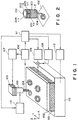
- Fig. 1 is an illustration showing a preferred embodiment of the present invention.
- the substrate electrode 101 an epitaxial growth surface of gold or a graphite cleavage surface onto a flat substrate such as glass or mica may be employed.
- the recording layer 102 employing squarylium-bis-6-octylazulene (hereinafter abbreviated as SOAZ), a built-up film of two layers of monomolecular films is formed according to the Langmuir-Blodgett's method on the substrate electrode 101 surface.
- SOAZ squarylium-bis-6-octylazulene
- the probe electrode 104 is made proximate to a distance of less than a nanometer relative to the desired position of the recording layer 102.
- an electroconductive material with the tip end being sharp such as a tungsten wire subjected to electrolytic polishing, a platinum wire, etc. mechanically cut may be used.
- a PZT device may be employed, a voltage (bias voltage) of about 0.1 to 1 V is applied by the bias power source 105 between the substrate electrode 101 and the probe electrode 104, the probe current flowing between the both is detected by the probe current detector 106, and the distance between the probe electrode 104 and the substrate electrode 101 is controlled by the servo circuit 107 so that the probe current value Ip may be substantially constant between 10 -10 A ⁇ Ip ⁇ 10 -8 A.
- Recording/erasing are practiced as described below.
- the signal from the recording/erasing signal generator 108 is applied between the substrate electrode 101 and the probe electrode 104, and recording/erasing are practiced at a desired position of the recording layer 102 proximate to the tip end of the probe electrode 104.
- a bias voltage for reading is applied between the substrate electrode 101 and the probe electrode 104 by the bias power source 105, reproducing is effected at a desired position of the recording layer 102 proximate to the tip end of the probe electrode 104.
- the electric memory effect refers to at least two different resistance states corresponding to voltage application, which respective states are freely transitionable to each other by application of a voltage or a current exceeding the threshold value which changes the electroconductivity of the recording layer, and which respective states obtained are capable of retaining their states so long as a voltage or a current not exceeding the threshold value is applied.
- the material constituting the recording layer may include those as set forth below.
- Examples of the structure of the dye having a suitable ⁇ -electron system for the present invention may include dyes having porphylline skelton such as phthalocyanine, tetraphenylporphine, azulene type dyes having squarylium group and croconicmethine group as the binding chain, and dyes similar to cyanine type having 2 nitrogen containing heterocyclic rings such as quinoline, benzothiazole, benzooxazole, etc.
- dyes having porphylline skelton such as phthalocyanine, tetraphenylporphine, azulene type dyes having squarylium group and croconicmethine group as the binding chain
- dyes similar to cyanine type having 2 nitrogen containing heterocyclic rings such as quinoline, benzothiazole, benzooxazole, etc.
- condensed polycyclic aromatics such as cyanine dyes, anthracene and pyrene, etc.
- chain compounds comprising polymers of aromatic rings and heterocyclic rings compound, and polymers of diacetylene groups, further derivatives of tetraquinodimethane or tetrathiafulvalene and homologues thereof, and charge transfer complexes thereof, and further metal complex compounds such as ferrocene, trisbipyridine ruthenium complexes, etc.
- various high milecular weight materials can be also used.
- addition polymers such as polyacrylic acid derivatives, etc., condensation polymers such as polyimide, polyphenylene, polythiophene, etc., ring-opened polymers such as nylon, etc., or biological high molecular weight materials such as polypeptide, bacteriorhodopsin, etc. can be included.
- the circular scanning driving mechanism 109 of the probe electrode 104 is, for example, a cylindrical piezoelectric device having a divided electrode pattern as shown in Fig. 2, and actuating the probe electrode 104 in spiral form is achieved by applying the voltages as shown below on the respective divided electrodes 201 to 204 by the circular scanning driving circuit 110:
- V +X V(t)sin ⁇ t + V OS
- V -X -V(t)sin ⁇ t - V OS
- the initial medium 301 is previously formatted. That is, at approximately the center portions of the respective recording regions a-1, a-2, ..., b-1, b-2, ..., recording bits of the format pattern 302 are recorded as shown in Fig. 3 (b).
- registration of the probe electrode 104 to the center of each recording region is effected by the coarse adjustment driving circuit 112, the coarse adjustment mechanism 113 following the set value of the microcomputer 111, and driving of the probe electrode 104 during recording of the circular format pattern 302 by the circular driving circuit 110, the circular driving mechanism 109, following the set value of the microcomputer 111.
- the address information of each region is recorded in the format pattern.
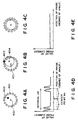
- the method of accessing the probe electrode 104 to a desired region of the recording medium 102 after formatting is practiced first by registration of the probe electrode tip end 402 inside of the format pattern of said recording region as shown in Fig. 4 (Fig. 4A).
- the registration is effected by the coarse adjustment mechanism 113, but since it is guaranteed that the probe electrode tip end will necessarily enter inside of the format pattern 403, the radius of the format pattern is required to be larger than the registration precision of the coarse adjustment mechanism.
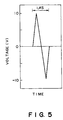
- Fig. 4B circular scanning of the probe electrode tip end 402 (the radius of circular scanning is taken slightly smaller than the radius of the format pattern) is performed. At this time, if the center 401 of the recording region and the center 404 of circular scanning are not coincident, the probe electrode can detect the format pattern bit 403 as shown in Fig.
- recording is performed by circular scanning of the probe electrode 303 around the format pattern as shown in Fig. 3 (c) (here of the recording region b-2).
- recording is performed onto another recording region after completion of recording onto the desired region, after making the center of circular scanning of the probe electrode coincident with the center of the desired recording region, recording is performed similarly.
- the probe electrode tip end is subjected to registration inside of the format pattern of the desired recording region, and circular scanning is performed to make the center of the recording region coincident with the center of circular scanning. Then, as shown in Fig. 3 (d), the data recorded around the format pattern (here of the recording region a-2) is reproduced by circular scanning of the probe electrode 303.
- the recording bit size became about 10 nm, the format pattern size about 100 nm, the size of one recording region about 10 ⁇ m, the size of the whole recording region about 10 mm square, the registration precision of the circular driving mechanism about 0.1 nm, the registration precision of the coarse adjustment mechanism about 10 nm, whereby recording and reproducing of high density large capacity (about 10 12 bit/cm 2 ) and high speed access (10 ms or less) were rendered possible.
- an information processing device of large capacity capable of high speed access having a registration precision of 1 nanometer or less can be realized with a simple constitution without performing complicated processing such as two-dimensional data processing, etc.
- no pattern of a special shape (different from the recording bit and the arraying shape of the recording bits) is required to be provided on the format pattern as the positional standard pattern, and the same pattern as the arraying shape of the recording bits can be used as such as the positional standard pattern.
Landscapes
- Semiconductor Memories (AREA)
- Measurement Of Length, Angles, Or The Like Using Electric Or Magnetic Means (AREA)
- Optical Recording Or Reproduction (AREA)
Claims (10)
- Procédé d'accès de l'électrode de sonde (104) d'un microscope à balayage à effet tunnel (STM) à une configuration de format (302) dans au moins une zone d'enregistrement (a-1, a-2,...) d'un support d'enregistrement (301), le procédé comprenant
une étape d'ajustement approximatif, lors de laquelle l'électrode de sonde (104) est positionnée dans ladite zone d'enregistrement (a-1, a-2, ...) et une étape d'ajustement précis, lors de laquelle l'électrode de sonde (104) est amenée dans une position prédéterminée par rapport à ladite configuration de format (302), par détection de variations du courant produit par effet tunnel, qui apparaissent entre l'électrode de sonde et le support,
caractérisé en ce queladite configuration de format située dans ladite au moins une région d'enregistrement (a-1, a-2, ....) possède une forme circulaire, destinée à être entourée par une configuration de données d'information,l'électrode de sonde (104) étant positionnée, lors de l'étape d'ajustement approximatif, en un endroit à l'intérieur de la zone de ladite configuration de format de forme circulaire,l'électrode de sonde (104) étant mise en balayage circulairement, lors de l'étape d'ajustement précis, au dessus de la configuration de format avec un rayon inférieur au rayon de la configuration de format (302),pour détecter ainsi des positions, dans lesquelles le trajet de balayage de l'électrode de sonde chevauche la configuration de format circulaire (302), obtenir, à partir de ces positions détectées, la valeur de déviation du centre du trajet de balayage circulaire de l'électrode de sonde (104) par rapport au centre de la configuration de format (302), déplacer l'électrode de sonde (104) de façon correspondante. - Procédé selon la revendication 1, selon lequel le support d'enregistrement (301) possède un effet de mémoire électrique, selon lequel l'électroconductivité d'une partie du support (301) varie en fonction d'une tension appliquée entre l'électrode de sonde (104) et le support d'enregistrement (301).
- Procédé selon la revendication 2, selon lequel l'enregistrement d'une information est exécuté par application d'une tension dépassant une tension de seuil, qui fait apparaître l'effet de mémoire électrique, entre l'électrode de sonde (104) et le support (301).
- Procédé selon la revendication 3, selon lequel la tension appliquée est une tension impulsionnelle.
- Procédé selon la revendication 2, selon lequel la lecture d'une information est exécutée par application d'une tension qui ne dépasse pas une tension de seuil, qui fait apparaître l'effet de mémoire électrique, entre l'électrode de sonde (104) et le support d'enregistrement (301).
- Procédé selon la revendication 5, selon lequel la tension appliquée est une tension de polarisation.
- Procédé selon la revendication 2, selon lequel un effacement de l'information est exécuté par application d'une tension dépassant une tension de seuil, qui fait apparaître l'effet de mémoire électrique, entre l'électrode de sonde et le support d'enregistrement (301).
- Système de microscope à balayage à effet tunnel comprenant :un support d'enregistrement portant une configuration de format dans au moins une zone d'enregistrement (a-1, a-2, ...);une électrode de sonde (104);des moyens (105) de production d'une tension de polarisation pour appliquer une tension entre ladite électrode de sonde (104) et ledit support (301);des moyens (106) de détection du courant produit par effet tunnel, pour détecter un courant produit par effet tunnel entre ladite électrode de sonde (104) et ledit support (301);un mécanisme d'entraînement (112, 103, 109) pour déplacer ladite électrode de sonde (104) pour l'amener à l'intérieur de ladite zone d'enregistrement (a-1, a-2, ...);des moyens (106, 111) de détection de variations du courant produit par effet tunnel pour détecter les variations du courant produit par effet tunnel qui apparaissent lorsque ladite électrode de sonde (104) croise ladite configuration de format (302); etdes moyens pour positionner l'électrode de sonde (104) dans une région prédéterminée par rapport à ladite configuration de format (302) en utilisant lesdites variations détectées du courant produit par effet tunnel; ledit système étant caractérisé en ce queladite configuration de format dans ladite au moins une région d'enregistrement (a-1, a-2, ...) possède une forme circulaire destinée à être entourée par une configuration de données d'information, eten ce qu'il comporte en outre des moyens pour positionner l'électrode de sonde (104) en un endroit à l'intérieur de la zone de ladite configuration de format de forme circulaire,des moyens pour amener l'électrode de sonde (104) à effectuer un balayage circulaire de la configuration de format avec un rayon inférieur au rayon de la configuration de format (302),des moyens pour détecter des positions, dans lesquelles le trajet de balayage de l'électrode de sonde chevauche la configuration de format circulaire (302), et des moyens pour obtenir, de ces positions détectées, la valeur de déviation du centre du trajet de balayage circulaire de l'électrode de sonde (104) par rapport au centre de la configuration de format (302),et des moyens pour déplacer l'électrode de sonde (104) de façon correspondante.
- Système selon la revendication 8, dans lequel ledit support d'enregistrement (301) produit un effet de mémoire électrique, selon lequel l'électroconductivité d'une partie dudit support (301) varie en fonction d'une tension appliquée entre ladite électrode de sonde (104) et ledit support (301).
- Système selon la revendication 8 ou 9, comprenant des moyens (108) de production d'un signal d'enregistrement / d'effacement pour enregistrer et effacer une information dans ledit support (301).
Applications Claiming Priority (4)
| Application Number | Priority Date | Filing Date | Title |
|---|---|---|---|
| JP23365189 | 1989-09-07 | ||
| JP233651/89 | 1989-09-07 | ||
| JP221708/90 | 1990-08-22 | ||
| JP22170890A JP2744341B2 (ja) | 1989-09-07 | 1990-08-22 | アクセス方法及びこれを利用した情報処理方法、情報処理装置 |
Publications (3)
| Publication Number | Publication Date |
|---|---|
| EP0416882A2 EP0416882A2 (fr) | 1991-03-13 |
| EP0416882A3 EP0416882A3 (en) | 1992-05-20 |
| EP0416882B1 true EP0416882B1 (fr) | 1997-03-05 |
Family
ID=26524450
Family Applications (1)
| Application Number | Title | Priority Date | Filing Date |
|---|---|---|---|
| EP90309686A Expired - Lifetime EP0416882B1 (fr) | 1989-09-07 | 1990-09-05 | Stockage, accès et traitement d'information |
Country Status (4)
| Country | Link |
|---|---|
| US (1) | US5222060A (fr) |
| EP (1) | EP0416882B1 (fr) |
| CA (1) | CA2024648C (fr) |
| DE (1) | DE69030040T2 (fr) |
Families Citing this family (24)
| Publication number | Priority date | Publication date | Assignee | Title |
|---|---|---|---|---|
| EP0522168A1 (fr) * | 1991-01-11 | 1993-01-13 | Hitachi, Ltd. | Appareil et procede d'usinage d'atomes de surface |
| JP2744359B2 (ja) * | 1991-04-24 | 1998-04-28 | キヤノン株式会社 | 情報再生及び/又は情報記録装置 |
| JP3029143B2 (ja) * | 1991-06-11 | 2000-04-04 | キヤノン株式会社 | 情報再生方法 |
| DE69228103T2 (de) * | 1991-10-15 | 1999-07-15 | Canon K.K., Tokio/Tokyo | Informationsverarbeitungsgerät mit Spurausrichtungsmechanismus |
| JPH06187675A (ja) * | 1992-09-25 | 1994-07-08 | Canon Inc | 情報処理装置、及びそれを用いる情報処理方法 |
| JP3581475B2 (ja) * | 1995-02-13 | 2004-10-27 | キヤノン株式会社 | 情報処理装置 |
| US5757760A (en) * | 1996-01-18 | 1998-05-26 | Canon Kabushiki Kaisha | Information recording and/or reproducing apparatus and method for performing recording and/or reproduction of information by using probe |
| JP3679525B2 (ja) * | 1996-10-07 | 2005-08-03 | キヤノン株式会社 | 情報記録再生装置、および情報記録再生方法 |
| JP3827105B2 (ja) * | 1997-02-12 | 2006-09-27 | 株式会社モリタユージー | 天井裏設置型自動消火装置 |
| US7260051B1 (en) | 1998-12-18 | 2007-08-21 | Nanochip, Inc. | Molecular memory medium and molecular memory integrated circuit |
| US6324091B1 (en) | 2000-01-14 | 2001-11-27 | The Regents Of The University Of California | Tightly coupled porphyrin macrocycles for molecular memory storage |
| AU764750B2 (en) * | 1999-07-01 | 2003-08-28 | North Carolina State University | High density non-volatile memory device |
| US6381169B1 (en) | 1999-07-01 | 2002-04-30 | The Regents Of The University Of California | High density non-volatile memory device |
| WO2002077633A1 (fr) | 2001-03-23 | 2002-10-03 | The Regents Of The University Of California | Ampérométrie et voltampérométrie du potentiel d'un circuit ouvert |
| US6728129B2 (en) * | 2002-02-19 | 2004-04-27 | The Regents Of The University Of California | Multistate triple-decker dyads in three distinct architectures for information storage applications |
| US7233517B2 (en) | 2002-10-15 | 2007-06-19 | Nanochip, Inc. | Atomic probes and media for high density data storage |
| US20050232061A1 (en) | 2004-04-16 | 2005-10-20 | Rust Thomas F | Systems for writing and reading highly resolved domains for high density data storage |
| US20060238696A1 (en) * | 2005-04-20 | 2006-10-26 | Chien-Hui Wen | Method of aligning negative dielectric anisotropic liquid crystals |
| US20070041237A1 (en) * | 2005-07-08 | 2007-02-22 | Nanochip, Inc. | Media for writing highly resolved domains |
| US7463573B2 (en) | 2005-06-24 | 2008-12-09 | Nanochip, Inc. | Patterned media for a high density data storage device |
| US7367119B2 (en) * | 2005-06-24 | 2008-05-06 | Nanochip, Inc. | Method for forming a reinforced tip for a probe storage device |
| US7309630B2 (en) | 2005-07-08 | 2007-12-18 | Nanochip, Inc. | Method for forming patterned media for a high density data storage device |
| US7995216B2 (en) * | 2008-07-02 | 2011-08-09 | Ut-Battelle, Llc | Control of the positional relationship between a sample collection instrument and a surface to be analyzed during a sampling procedure with image analysis |
| CN102866266B (zh) * | 2012-09-07 | 2014-08-06 | 上海交通大学 | 三维微驱四电极可置换探头 |
Family Cites Families (14)
| Publication number | Priority date | Publication date | Assignee | Title |
|---|---|---|---|---|
| US4087842A (en) * | 1976-11-05 | 1978-05-02 | Graham Magnetics Inc. | Recording track eccentricity compensation method and means |
| DE3679319D1 (de) * | 1986-05-27 | 1991-06-20 | Ibm | Speichereinheit mit direktem zugriff. |
| JP2556491B2 (ja) * | 1986-12-24 | 1996-11-20 | キヤノン株式会社 | 記録装置及び記録法 |
| JP2556492B2 (ja) * | 1986-12-24 | 1996-11-20 | キヤノン株式会社 | 再生装置及び再生法 |
| JP2557964B2 (ja) * | 1988-01-22 | 1996-11-27 | インターナシヨナル・ビジネス・マシーンズ・コーポレイーシヨン | データ記憶装置 |
| JP2760508B2 (ja) * | 1988-06-23 | 1998-06-04 | 工業技術院長 | 走査型トンネル顕微鏡 |
| NL8802335A (nl) * | 1988-09-21 | 1990-04-17 | Philips Nv | Werkwijze en inrichting voor het op sub-mikron schaal bewerken van een materiaal-oppervlak. |
| JP2896794B2 (ja) * | 1988-09-30 | 1999-05-31 | キヤノン株式会社 | 走査型トンネル電流検出装置,走査型トンネル顕微鏡,及び記録再生装置 |
| JP2547869B2 (ja) * | 1988-11-09 | 1996-10-23 | キヤノン株式会社 | プローブユニット,該プローブの駆動方法及び該プローブユニットを備えた走査型トンネル電流検知装置 |
| US5091880A (en) * | 1989-02-02 | 1992-02-25 | Olympus Optical Co., Ltd. | Memory device |
| JP2821005B2 (ja) * | 1989-10-02 | 1998-11-05 | オリンパス光学工業株式会社 | 微細表面形状計測装置 |
| JPH0687003B2 (ja) * | 1990-02-09 | 1994-11-02 | 株式会社日立製作所 | 走査型トンネル顕微鏡付き走査型電子顕微鏡 |
| US5066858A (en) * | 1990-04-18 | 1991-11-19 | Digital Instruments, Inc. | Scanning tunneling microscopes with correction for coupling effects |
| US5053699A (en) * | 1990-05-25 | 1991-10-01 | Texas Instruments Incorporated | Scanning electron microscope based parametric testing method and apparatus |
-
1990
- 1990-09-05 DE DE69030040T patent/DE69030040T2/de not_active Expired - Fee Related
- 1990-09-05 US US07/577,551 patent/US5222060A/en not_active Expired - Lifetime
- 1990-09-05 EP EP90309686A patent/EP0416882B1/fr not_active Expired - Lifetime
- 1990-09-05 CA CA002024648A patent/CA2024648C/fr not_active Expired - Fee Related
Also Published As
| Publication number | Publication date |
|---|---|
| DE69030040T2 (de) | 1997-07-03 |
| US5222060A (en) | 1993-06-22 |
| EP0416882A3 (en) | 1992-05-20 |
| CA2024648C (fr) | 1994-10-18 |
| EP0416882A2 (fr) | 1991-03-13 |
| CA2024648A1 (fr) | 1991-03-08 |
| DE69030040D1 (de) | 1997-04-10 |
Similar Documents
| Publication | Publication Date | Title |
|---|---|---|
| EP0416882B1 (fr) | Stockage, accès et traitement d'information | |
| US5396483A (en) | Recording medium having a track and electrode layer provided and recording and reproducing device and system using same | |
| EP0416920B1 (fr) | Procédé et dispositif de traitement d'information | |
| EP0471511B1 (fr) | Capteur de type cantilever et appareil de traitement d'informations équipé de ce capteur | |
| JP2884447B2 (ja) | カンチレバー型プローブ、及びこれを用いた走査型トンネル顕微鏡、情報処理装置 | |
| US5389475A (en) | Recording medium and information-erasing method | |
| US5623476A (en) | Recording device and reproduction device | |
| US7221639B2 (en) | Pickup device | |
| EP0334677B1 (fr) | Dispositif d'enregistrement d'informations et procédé d'enregistrement et de reproduction d'informations | |
| EP0475365B1 (fr) | Méthode d'asservissement pour appareil de mémorisation | |
| EP0551965B1 (fr) | Appareil d'enregistrement et appareil de reproduction | |
| JP2744341B2 (ja) | アクセス方法及びこれを利用した情報処理方法、情報処理装置 | |
| JP2930449B2 (ja) | トラッキング方法 | |
| JP2556520B2 (ja) | 記録装置及び記録法 | |
| EP0640963A1 (fr) | Procédé d'enregistrement/de reproduction et appareil utilisant échantillon | |
| JP2862352B2 (ja) | 情報処理方法及び情報処理装置 | |
| JP2866165B2 (ja) | 記録媒体およびその製造方法、情報処理方法、情報処理装置 | |
| JP3220914B2 (ja) | 記録媒体製造方法 | |
| CA2024725C (fr) | Methode et dispositif de traitement de donnees | |
| JPH04129043A (ja) | プローブユニット、該プローブユニットを備えた情報処理装置及び情報処理方法 | |
| JPH04223203A (ja) | カンチレバー型プローブ、これを用いた情報処理装置及び情報処理方法 |
Legal Events
| Date | Code | Title | Description |
|---|---|---|---|
| PUAI | Public reference made under article 153(3) epc to a published international application that has entered the european phase |
Free format text: ORIGINAL CODE: 0009012 |
|
| 17P | Request for examination filed |
Effective date: 19901231 |
|
| AK | Designated contracting states |
Kind code of ref document: A2 Designated state(s): BE CH DE FR GB IT LI NL SE |
|
| PUAL | Search report despatched |
Free format text: ORIGINAL CODE: 0009013 |
|
| AK | Designated contracting states |
Kind code of ref document: A3 Designated state(s): BE CH DE FR GB IT LI NL SE |
|
| 17Q | First examination report despatched |
Effective date: 19940112 |
|
| GRAG | Despatch of communication of intention to grant |
Free format text: ORIGINAL CODE: EPIDOS AGRA |
|
| GRAH | Despatch of communication of intention to grant a patent |
Free format text: ORIGINAL CODE: EPIDOS IGRA |
|
| GRAH | Despatch of communication of intention to grant a patent |
Free format text: ORIGINAL CODE: EPIDOS IGRA |
|
| GRAA | (expected) grant |
Free format text: ORIGINAL CODE: 0009210 |
|
| AK | Designated contracting states |
Kind code of ref document: B1 Designated state(s): BE CH DE FR GB IT LI NL SE |
|
| PG25 | Lapsed in a contracting state [announced via postgrant information from national office to epo] |
Ref country code: NL Free format text: LAPSE BECAUSE OF FAILURE TO SUBMIT A TRANSLATION OF THE DESCRIPTION OR TO PAY THE FEE WITHIN THE PRESCRIBED TIME-LIMIT Effective date: 19970305 Ref country code: LI Effective date: 19970305 Ref country code: CH Effective date: 19970305 Ref country code: BE Effective date: 19970305 |
|
| REG | Reference to a national code |
Ref country code: CH Ref legal event code: EP |
|
| REF | Corresponds to: |
Ref document number: 69030040 Country of ref document: DE Date of ref document: 19970410 |
|
| ET | Fr: translation filed | ||
| ITF | It: translation for a ep patent filed | ||
| PG25 | Lapsed in a contracting state [announced via postgrant information from national office to epo] |
Ref country code: SE Effective date: 19970605 |
|
| NLV1 | Nl: lapsed or annulled due to failure to fulfill the requirements of art. 29p and 29m of the patents act | ||
| RIN2 | Information on inventor provided after grant (corrected) |
Free format text: KURODA, RYO, C/O CANON KABUSHIKI KAISHA * NOSE, HIROYASU, C/O CANON KABUSHIKI KAISHA * MIYAZAKI, TOSHIHIKO, C/O CANON KABUSHIKI KAISHA * OGUCHI, TAKAHIRO, C/O CANON KABUSHIKI KAISHA * SAKAI, KUNIHIRO, C/O CANON KABUSHIKI KAISHA |
|
| REG | Reference to a national code |
Ref country code: CH Ref legal event code: PL |
|
| PLBE | No opposition filed within time limit |
Free format text: ORIGINAL CODE: 0009261 |
|
| STAA | Information on the status of an ep patent application or granted ep patent |
Free format text: STATUS: NO OPPOSITION FILED WITHIN TIME LIMIT |
|
| 26N | No opposition filed | ||
| REG | Reference to a national code |
Ref country code: GB Ref legal event code: IF02 |
|
| PGFP | Annual fee paid to national office [announced via postgrant information from national office to epo] |
Ref country code: GB Payment date: 20040823 Year of fee payment: 15 |
|
| PGFP | Annual fee paid to national office [announced via postgrant information from national office to epo] |
Ref country code: FR Payment date: 20040927 Year of fee payment: 15 |
|
| PGFP | Annual fee paid to national office [announced via postgrant information from national office to epo] |
Ref country code: DE Payment date: 20041124 Year of fee payment: 15 |
|
| PG25 | Lapsed in a contracting state [announced via postgrant information from national office to epo] |
Ref country code: IT Free format text: LAPSE BECAUSE OF NON-PAYMENT OF DUE FEES;WARNING: LAPSES OF ITALIAN PATENTS WITH EFFECTIVE DATE BEFORE 2007 MAY HAVE OCCURRED AT ANY TIME BEFORE 2007. THE CORRECT EFFECTIVE DATE MAY BE DIFFERENT FROM THE ONE RECORDED. Effective date: 20050905 Ref country code: GB Free format text: LAPSE BECAUSE OF NON-PAYMENT OF DUE FEES Effective date: 20050905 |
|
| PG25 | Lapsed in a contracting state [announced via postgrant information from national office to epo] |
Ref country code: DE Free format text: LAPSE BECAUSE OF NON-PAYMENT OF DUE FEES Effective date: 20060401 |
|
| GBPC | Gb: european patent ceased through non-payment of renewal fee |
Effective date: 20050905 |
|
| PG25 | Lapsed in a contracting state [announced via postgrant information from national office to epo] |
Ref country code: FR Free format text: LAPSE BECAUSE OF NON-PAYMENT OF DUE FEES Effective date: 20060531 |
|
| REG | Reference to a national code |
Ref country code: FR Ref legal event code: ST Effective date: 20060531 |