EP0416886B1 - Bildaufzeichnungsgerät - Google Patents
Bildaufzeichnungsgerät Download PDFInfo
- Publication number
- EP0416886B1 EP0416886B1 EP90309691A EP90309691A EP0416886B1 EP 0416886 B1 EP0416886 B1 EP 0416886B1 EP 90309691 A EP90309691 A EP 90309691A EP 90309691 A EP90309691 A EP 90309691A EP 0416886 B1 EP0416886 B1 EP 0416886B1
- Authority
- EP
- European Patent Office
- Prior art keywords
- data
- signal
- image
- pixel
- resolution
- Prior art date
- Legal status (The legal status is an assumption and is not a legal conclusion. Google has not performed a legal analysis and makes no representation as to the accuracy of the status listed.)
- Expired - Lifetime
Links
Images




















Classifications
-
- G—PHYSICS
- G06—COMPUTING OR CALCULATING; COUNTING
- G06T—IMAGE DATA PROCESSING OR GENERATION, IN GENERAL
- G06T3/00—Geometric image transformations in the plane of the image
- G06T3/40—Scaling of whole images or parts thereof, e.g. expanding or contracting
- G06T3/4007—Scaling of whole images or parts thereof, e.g. expanding or contracting based on interpolation, e.g. bilinear interpolation
-
- G—PHYSICS
- G06—COMPUTING OR CALCULATING; COUNTING
- G06K—GRAPHICAL DATA READING; PRESENTATION OF DATA; RECORD CARRIERS; HANDLING RECORD CARRIERS
- G06K15/00—Arrangements for producing a permanent visual presentation of the output data, e.g. computer output printers
- G06K15/02—Arrangements for producing a permanent visual presentation of the output data, e.g. computer output printers using printers
-
- G—PHYSICS
- G06—COMPUTING OR CALCULATING; COUNTING
- G06T—IMAGE DATA PROCESSING OR GENERATION, IN GENERAL
- G06T5/00—Image enhancement or restoration
- G06T5/20—Image enhancement or restoration using local operators
-
- H—ELECTRICITY
- H04—ELECTRIC COMMUNICATION TECHNIQUE
- H04N—PICTORIAL COMMUNICATION, e.g. TELEVISION
- H04N1/00—Scanning, transmission or reproduction of documents or the like, e.g. facsimile transmission; Details thereof
- H04N1/40—Picture signal circuits
- H04N1/40068—Modification of image resolution, i.e. determining the values of picture elements at new relative positions
-
- G—PHYSICS
- G06—COMPUTING OR CALCULATING; COUNTING
- G06K—GRAPHICAL DATA READING; PRESENTATION OF DATA; RECORD CARRIERS; HANDLING RECORD CARRIERS
- G06K2215/00—Arrangements for producing a permanent visual presentation of the output data
- G06K2215/0002—Handling the output data
- G06K2215/004—Generic data transformation
- G06K2215/0054—Geometric transformations, e.g. on rasterised data
- G06K2215/0057—Sizing and resolution changes
-
- G—PHYSICS
- G06—COMPUTING OR CALCULATING; COUNTING
- G06K—GRAPHICAL DATA READING; PRESENTATION OF DATA; RECORD CARRIERS; HANDLING RECORD CARRIERS
- G06K2215/00—Arrangements for producing a permanent visual presentation of the output data
- G06K2215/0002—Handling the output data
- G06K2215/0062—Handling the output data combining generic and host data, e.g. filling a raster
- G06K2215/0071—Post-treatment of the composed image, e.g. compression, rotation
Definitions
- the present invention relates to an image recording apparatus, and, more particularly, to an image recording apparatus for recording an image on a recording medium in accordance with image data supplied from a host computer or the like.
- An apparatus of the type described above exhibits a multiplicity of advantage such as high image quality and low noise.
- the excellent image quality realized by an apparatus of the type described above has been rapidly widened the market of the DTP (Desk Top Publishing).
- Fig. 1 is a structural view which schematically illustrates an ordinary laser beam printer.
- a laser beam printer 300 comprises a printer controller 100 and a printer engine portion 200.
- the printer controller 100 receives code data (for example, page writing language) or image data so as to develop the image data in the bit map memory thereof, the data thus developed being then transmitted to the printer engine portion 200.
- the printer engine portion 200 turns on/off a laser device in accordance with data supplied from the printer controller 100.
- a laser beam is generated so as to be applied to the side surface of a polygonal mirror which is being rotated at a predetermined speed.
- the surface of a photosensitive drum is applied with the laser beam in the main scanning direction.
- the printer engine portion 200 usually arranged to have a resolution of 300 dpi.
- the printer engine portion 200 has recently been arranged in such a manner that the resolution of the printed image has been doubled or higher. Furthermore, the gradation expression has been realized.
- the gradation can be expressed by a pulse width modulation (to be abbreviated to a "PWM” method hereinafter) method. That is, the laser device is operated for a duration corresponding to the density, and the gradation is expressed by the area of the dot which has thereby been formed.
- PWM pulse width modulation
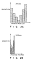
- Fig. 2A illustrates the relationship between the position of the dot on one line and the density in the case where the resolution is 300 dpi. If the image in accordance with the same data is printed by a 1200 dpi printer, the relationship becomes as shown in Fig. 2B, resulting the lateral length of the image (similar to the longitudinal length) to become a quarter of the desired length.
- a gradation image can be recorded by receiving multivalued data from the host computer 500.
- a binary image is recorded at 600 dpi.
- the multivalued image is recorded in such a manner that it is recorded at about a density of 150 dpi (150 lines) by collecting 4 x 4 dots, each of which is 600 dpi, into one unit.
- characters and lines can be recorded with high resolution exhibited and the half tone image exhibiting an excellent gradation can be recorded.
- Fig. 37 is a block diagram which illustrates a portion of the printer engine portion 200.
- the printer engine 200 is arranged to have the resolution of 300 dpi, and the resolution at the time of the PWM processing is 150 dpi.
- the printer controller 100 transmits 6-bits multivalued video signals VD00 to VD05, binary video signal VIDEO and multivalue/binary selection signal M/B to the printer engine portion 200 in synchronization with image clock VCLK which corresponds to a resolution of 300 dpi.
- image clock VCLK which corresponds to a resolution of 300 dpi.
- the above-described signals are synchronized with the image clock VCLK so as to be fetched by a flip-flop 55.
- a pulse width modulation circuit 56 generates signal PW the pulse width of which has been modulated at 150 dpi unit in response to the multivalued video signals VD00 to VD05, the generated signal PW being then supplied to input terminal A of a selector 57.
- the binary video signal VIDEO is synchronized with the signal VCLK in the flip-flop 55 so as to be supplied to other input terminal B of the selector 57.
- the multivalue/binary selection signal M/B acts to select that the pixel to be printed (a subject pixel) is printed as multivalued data or the same is printed as binary data.
- the selector 57 determines that the multivalued printing is performed when the multivalue/binary selection signal M/B is "0" so that it selects the input A of the selector 57. Furthermore, when the above-described signal is "1", it determines that the binary (character or line) printing is performed and it selects and transmits the input B of the selector 57.
- Output Y from the selector 57 serves as laser drive signal LD so that the printing is performed by a known electrophotographic method.
- the image is printed at a resolution of 150 dpi and the text is printed at a resolution of 300 dpi. Therefore, the printed image is formed by the mixture of pixels having different resolutions.
- the quality of the processed document may be adversely influenced by the difference between the resolutions of the multivalued data and the binary data.
- page writing language for example, PCL, post-script, DDL or the like
- an outline 58 of an binary image is instructed.
- the outline 58 is generated at the resolution of 300 dpi which is the resolution arranged for the printer engine 200.
- the inside portion (the lower right portion in the drawing) of the outline 58 is applied with gray (multivalued data).
- the resolution becomes 150 dpi.
- the above-described region is furthermore applied with black, which is in a binary mode, as an alternative to gray.
- black since it is the text data, the resolution becomes 300 dpi.
- the present invention is concerned with providing an image recording apparatus capable of recording an image of a desired size and excellent quality even if one of a plurality of available application softwares capable of operating on a host computer or the like are used as it is.
- EP-A-0,232,081 discloses image processing apparatus which incorporates interpolation.
- an image processing apparatus comprising: input means for inputting multi-valued data representing pixels and having a first resolution; and means for converting the input data into multi-valued data having a second resolution higher than said first resolution; and characterised in that: said converting means comprises means for comparing with a predetermined value the difference between input data representing two neighboring pixels; and converting the means converting the input data into multi-valued data of the second resolution representation in accordance with whether or not the difference between the input multi-valued data is larger than said predetermined value.
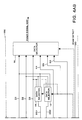
- Figs. 4AA and 4AB illustrate data conversion circuit positioned between the printer controller 100 and the printer engine portion 200 shown in Fig. 1.
- the printer controller 100 transmits a video signal for 300 dpi and 16 gradations.
- the data conversion circuit according to this embodiment and included in the printer engine portion 200 receives the above-described data so as to convert it into data for 1200 dpi and 16 gradations.
- the above-described printer engine portion 200 comprises a laser driver for modulating the laser beam in response to a video signal (dot information), a scanner for performing scanning by laser beams and photosensitive drum.
- the printer controller 100 transmits video signal VDO for 300 dpi and 16 gradations (four bits for a pixel) by a quantity for one line in synchronization with image clock VCLK to the printer engine portion 200 whenever it receives horizontal synchronizing signal HSYNC supplied from a horizontal synchronizing signal generating circuit 4.
- the horizontal synchronization signal generating circuit 4 includes a counter so as to transmit the horizontal synchronizing signal HSYNC when the counter counts 4 times known beam detect signal BD which serves as a synchronizing signal in the main scanning direction.
- the printer engine portion 200 forms, in the data conversion circuit to be described later, video signal VDO′ for 1200 dpi and 16 gradations by converting the video signal VDO for 300 dpi and 16 gradations supplied in synchronization with the image clock VCLK, the printer engine portion 200 then performing printing of 1200 dpi and 16 gradations in accordance with the signal VDO′.
- Reference numeral 1 represents a frequency multiplying circuit for multiplying the frequency of the image clock VCLK so that clock VCLK′ the frequency of which is four times that of the image clock VCLK is obtained.
- Reference numeral 5 represents an oscillating circuit for generating clock LCLK having the frequency which is 16 times the frequency of the image clock VCLK.
- Reference numerals 11, 12 and 13 represent switch circuits which respectively select the clock VCLK′ or LCLK so as to supply it as the writing or reading clock for each of line memories(LM) 6 to 8.
- the interpolating circuit 17 generates pixel data (video signal VD) having the pixels the number of which is four times in the main scanning direction by inserting interpolating data between supplied pixel data (video signal VDO) items for 300 dpi for one line. That is, the interpolating circuit 17 is a circuit for converting pixel data for 300 dpi in the main scanning direction into data for 1200 dpi.
- a demultiplexer 2 selects any of the line memories 6 to 8 in response to a signal supplied from a device control circuit 3 so as to supply the signal interpolated by the interpolating circuit 17 to the selected line memory.
- the horizontal synchronizing signal generating circuit 4 counts the signal BD so that it transmits the horizontal synchronizing signal HSYNC whenever it receives four BD signals.
- the device control circuit 3 supplies a selection, a writing and a reading signal for one line to the demultiplexer 2, each of the switching circuits 11 to 13 and each of data selectors 14 to 16, to be described later, so as to control the above-described elements.
- the video signal VD is written in any of the line memories 6 to 8 in accordance with the clock VCLK′. Furthermore, the video signal is read from each of the other line memories in accordance with the clock LCLK.
- the above-described operations are successively performed in such a manner that, for example, when the video signal is written to the line memory 6, the video signal is read from each of the line memories 7 and 8.
- the video signal VD is written to the line memory 7, while data stored in the line memories 6 and 8 is read from the same.
- the line memory 8 is brought into the writing mode, while the line memories 6 and 7 are brought to the reading mode. Then, the above-described line memories are successively switched between the writing mode and the reading modes.
- Each of the line memories 6 to 8 has the memory capacity of four times the 300 dpi data in the main scanning direction, that is, the data memory capacity of 1200 dpi in the main scanning direction.
- the description will be made hereinafter in such a manner that the video signals read from the respective line memories are called D1, D2 and D3.
- the data selectors 14 and 15 select two video signals selected from a group consisting of the video signals D1, D2 and D3 supplied from the line memories, which have been brought to the reading mode in response to the control signal supplied from the device control circuit 3 so as to transmit the two selected video signals to the interpolating circuit 10. For example, when the line memory 6 is in the writing mode, the line memories 7 and 8 are in the reading mode. Therefore, the data selector 14 selects the data D2 read from the line memory 7 so as to transmit it as signal DS1 to the interpolating circuit 10. The data selector 15 selects the data D3 read from the line memory 8 so as to transmit it as the signal DS2 to the interpolating circuit 10.
- the interpolating circuit 10 processes the supplied signals DS1 and DS2 in the manner to be described later so as to generate interpolated image data and transmit it as output signals Q1, Q2 and Q3.
- each of line memories 9a to 9c which store the respective output signals Q1, Q2 and Q3, is the same as that of each of the line memories 6 to 8.
- the clock LCLK is used when data is written/read from each of the line memories 9a to 9c.
- the above-described data writing/reading from the line memories 6 to 8 and 9a to 9c and the operation for selecting either the data selector 14 or 15 is controlled by the device control circuit 3.
- the data selector 16 selects any of the signals D1 to D3 read from the respective line memories 6 to 8 and any of the signals D4 to D6 read from the respective line memories 9a to 9c so as to transmit the selected signal as video signal VDO′. Also the above-described selection operation is controlled by the device control circuit 3.
- the pixel data items are 4 bits data VD00 to VD03. Then, description will be made with reference to the signal VD03.
- the signal VD03 is alternately latched by latches 23 and 24 in accordance with clock VCLK/2 formed by halving the clock VCLk by a divider 18.
- the other signals VD02 to VD00 are respectively and alternately latched by latches 20, 21 and 22. That is, data for neighboring two pixels supplied as 300 dpi data is stored by the latches 19 to 22. The data for two pixels thus latched is then added in an adder 25 so that a resulted carry bit (Cy) and the upper three bits are taken.
- the average of the supplied data can be obtained, the average value thus calculated being arranged to be the pixel positioned at the intermediate position between the supplied two pixels.
- each of the pixel data items latched by the respective latches 19 to 22 are subject, in adders 26 and 27, to an operation in which the average value with the output value supplied from the adder 25 is calculated.
- the adders 25, 26 and 27 generate three interpolated pixel data items between the neighboring two pixels in the main scanning direction supplied as the VDO signal.
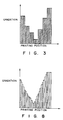
- the 300 dpi and 16 gradation data shown in Fig. 2A can be, as shown in Fig. 8, interpolated by smooth gradation data.
- the hatched section corresponds to the 300 dpi data supplied as the VDO signal, while the other portion corresponds to the pixel data obtained by the above-described interpolating processing.
- the data items are selected by a selection circuit 28 at every clock VCLK′ (having the frequency which is 4 times the frequency of the clock VCLK).
- the above-described interpolating circuit 17 performs the interpolation of the horizontal scanning, while the interpolating circuit 10 generates interpolated data in the vertical direction (in the sub-scanning direction) in accordance with data interpolated by the interpolating circuit 17.
- data for one horizontal scanning line is, as the signal DS1, supplied to an adder 29 included in the interpolating circuit 17.
- the adder 29 adds the pixel data items, which are included in the supplied signals DS1 and DS2 and the lateral positions of which are the same, so as to transmit the result of the addition as five-bits data.
- the upper four bits of the transmitted five bits are arranged to be data so that the average value of the two pixels on the neighboring lines can be obtained.
- the thus calculated average value is used as the pixel data for the line positioned between the two lines supplied from the printer controller 100.
- the averaged data DS1 and DS2 are further averaged by adders 30 and 31 so that three vertical interpolated data items are generated.
- the thus generated data items are stored in the respective line memories 9a to 9c before supplied to the data selector 16 as image data D4, D5 and D6.
- the data selector 16 selects one of the supplied image data D1 to D6 in accordance with the timing shown in Fig. 4B so as to transmit it as the image data VDO′ to a pulse width modulation circuit to be described later.
- Fig. 9 illustrates the structure of a circuit for modulating the pulse width and forming an image. The timing of each of the signals is shown in Figs. 10A and 10B.
- the four-bits video signal VDO′ horizontally and vertically interpolated and supplied from the data selector 16 is supplied to a look-up table (to be abbreviated to "LUT" hereinafter) 42 via a data line 100 in synchronization with a synchronizing clock 109.
- the LUT 42 corrects the supplied data to the data having proper density correction characteristics, the thus corrected image data being then transmitted to a D/A converter 32.
- the LUT 42 comprises a ROM having a 4-bits address input and a 4-bits data output.
- the D/A converter 32 converts 4-bits digital data supplied from the LUT 42 so as to transmit the analog signal to the minus input terminal of a comparator 36.
- a timing generating circuit 34 generates a timing signal 108 which is in synchronization with the synchronizing clock 109 formed in accordance with, for example, the signal BD so as to transmit it to a triangular wave generating circuit 35.
- the triangular circuit 35 generates a triangular signal 105 in synchronization with the thus supplied timing signal 108, the triangular signal 105 being supplied to the positive (plus) input terminal of the comparator 105.
- the timing at which the triangular signal 105 is generated from the triangular wave generating circuit 35 is shown in Fig. 10A.
- the comparator then makes a comparison between analog image data supplied to its input terminal and the triangular wave 105 so as to transmit an output signal 103 having the pulse width corresponding to the level of the input image data shown in Fig. 10B.
- a driver circuit 37 operates a semiconductor laser 38 in response to an output signal 103 so that the duration in which the semiconductor 38 is operated is controlled in accordance with the density.
- Reference numeral 39 represents a polygonal mirror for applying a scanning laser beam and 40 represents a photosensitive drum.
- Reference numeral 41 represents a detector (BD) for detecting the position which is scanned by the laser beam. The detection output signal supplied from the detector 41 is shaped by a waveform shaping circuit (omitted from illustration) so that it is made to be the above-described BD signal 107.
- the laser beam transmitted from the semiconductor laser 38 is reflected by the side surface of the polygonal mirror 39 which is being rotated at a predetermined speed so as to be laterally swept.
- the laser beam reflected by the polygonal mirror 39 is, by a lens or the like (omitted from illustration), imaged on the photosensitive surface of the photosensitive drum 40. Since the photosensitive drum 40 is rotated as illustrated, a two dimensional 1200 dpi static latent image is formed on the surface of the photosensitive drum 40. Then, an image is formed by a known electrophotography process so as to be transferred to the surface of recording paper.
- the three pixels are interpolated by unconditionally calculating the average value between the two pixel data items supplied from the printer controller 100.
- the two pixels are positioned at the edge of a character or a line.
- supplied two pixels A and B be used as it is as the data for interpolating the portion between the two supplied pixels A and B as an alternative to data the average of which has been calculated.
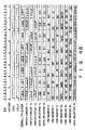
- Fig. 11A illustrates the status transition of the selection circuit 28 shown in Fig. 5.
- reference numeral 60 represents the state of the selection performed by the selection circuit 28, where symbol en represents a set of data bits e0, e2, e2 and e3 similarly to other symbols d n and c n .
- the selection circuit 28 selects d n , c n , b n , a n , b n , c n , d n and e n in this sequential order.
- the absolute value of the difference between the two pixels is subjected to a comparison with predetermined value T. If
- the determination may be made that the subject two pixels are positioned in the vicinity of the edge portion of the character or the line. Therefore, either of the pixels is selected and transmitted as the three interpolated data items generated between the pixels e n and a n . Since the equivalent circuit to the above-described inequality can be easily constituted by using a subtractor, a circuit for removing the sign from the result of the subtraction and a comparator, the detailed description is omitted here.
- the specific status transition of the selecting circuit 28 is shown in Fig. 11B.
- the selection circuit 28 has selected status e n . If the absolute value of the difference between the supplied pixel data e n and a n is larger than the predetermined value T, the selection circuit 28 selects e n three times so as to transmit them as the interpolated data. Then, the pixel a n is made to be the subject of the selection by a passage 62. If it is then determined that the absolute value between e n and a n is larger than the predetermined value T, an is selected three times by a passage 63 so as to transit the selection subject to the pixel e n .
- the selection subject is, similarly to Fig. 11A, transmitted as d n , c n , b n and a n or b n , c n , d n and e n in this sequential order if the result of the comparison is smaller than the predetermined value.
- an image having an excessive contrast for example, the outline of a character can be expressed clearly.
- the printer controller 100 having the printing density of 300 dpi and the printer engine portion 200 having the printing density of 1200 dpi are combined to each other.
- the present invention is not limited to a structure of the type described above. A similar effect can be obtained from a structure arranged in such a manner that, for example, a printer controller of the printing density of 150 dpi and the printer engine of the printing density of 600 dpi are combined to each other.
- the number of the dots to be interpolated is not limited according to this embodiment.
- the present invention can be effectively applied to a case in which a plurality of dots are interpolated or to a case in which a gradation data for example 256 gradations is processed.
- the half tone image may be expressed by the dither method as an alternative to the above-described pulse width modulation method.
- image data for a high density printer can be reproduced only with a reduced-capacity page memory, causing an economical effect to be obtained. Furthermore, the necessity of changing the conventional application for low-density printing operation acting on the host computer can be eliminated when high density printing is desired.
- interpolated data obtained by the calculation of the average value is not used.
- the supplied pixel data is used as the interpolated data as it is so that the edge portion of the character and the line can be clearly expressed.
- the interpolation rate (the number of pixels to be inserted between the supplied pixels) is calculated from the relationship between the thus instructed resolution and the resolution of the apparatus whereby the interpolation is performed in accordance with the result of the calculation.
- a second embodiment will be described in which a smoothing portion to be described later is provided for the printer engine portion 200 of the laser beam printer 300 shown in Fig. 1.
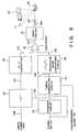
- Fig. 12 is a schematic block diagram which illustrates a variety of signals transmitted/received between the to controller 100 of the laser beam printer 300 and the printer engine portion 200 shown in Fig. 1 and a partial structure of the engine portion 200.
- 8-bits data 255 gradations
- multivalued pixel data is transmitted as substantially 150 dpi data since the same value data for 4 x 4 pixel region is transmitted.
- the printer engine portion 200 receives, from the printer controller, a vertical synchronizing signal (VSYNC) 2010, an image clock (VCLK) 2011, binary or multivalued data (8 bits data VD0 to VD7 of [00H] to [FFH] according to this embodiment) 2012, a multivalue/binary identification (M/B) signal 2013.
- a clock synchronizing and multiplying circuit 2020 creates a clock (LCLK) 2015 the frequency is four times from the vertical synchronising signal 2010 and the image clock 2011 so as to transmit it to a memory group 2021 and a smoothing portion 2022.
- the supplied image data 2012 is smoothed so as to be transmitted to a PWM processing portion 2023 and a binary processing portion 2024.
- the PWM processing portion 2023 creates a pulse width modulation signal in accordance with the supplied image data, while the binary processing portion 2024 binarizes the supplied image data.
- a signal obtained in the PWM processing portion 2023 or the binary processing portion 2024 is supplied to a laser driver 2025.
- the laser driver 2025 controls the operation of the semiconductor laser device which generates the laser beam.
- a horizontal synchronizing signal generator 2026 transmits the horizontal synchronizing signal (HSYNC) 2014 to the printer controller 100 when it receives a beam detect signal (BD) 2016 four times so as to notify it the timing of the printing start.
- HSELNC horizontal synchronizing signal
- BD beam detect signal
- the determination of the image data 2012 is made in such a manner that it is determined to be binary data when the binary/multivalue identification signal 2013 is "1", while it is determined to be multivalued data when the same is "0". In this case, it is assumed that the binary data is transmitted to the uppermost bit of the eight bits of the image data 2012.
- the supplied data of the resolution of 600 dpi is used as it is.
- the supplied data of the resolution of 600 dpi is converted into 150 dpi data.
- Fig. 13 is a block diagram which illustrates the structure of the above-described memory group 21 and the smoothing portion 22.
- 9-bits data consisting of the image data 2012 and the binary/multivalue identifying signal 2013 supplied from the controller 100 is written to one of memories 2030-1 to 2030-7 selected by a selector 2031 in accordance with an image clock 2011.
- the selector 2031 is switched in response to a horizontal synchronizing signal 2014.
- Each of the memories 2030-1 to 2030-7 has a capacity capable of storing images of 9-bits x 600 dpi for one line.
- reading from the residual six memories is performed in accordance with the clock 2015 which is four times the image clock 2011.
- data in the other memories 2030-1 to 2030-6 can be read and a read address counter 2033 is cleared every BD 2016. That is, data is successively read from the same memory four times during the operation of one horizontal synchronizing signal 2014.
- the data thus stored is subjected to a serial/parallel conversion so as to be supplied to a smoothing circuit 2035.
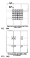
- the region to which a reference can be made, is a region including 3 x 3 pixels (9 pixels) of 150 dpi.
- the pixel data to which a reference is made by the smoothing circuit 2035 is shown in Figs. 14A to 14C.
- a pattern generator 2040 makes a reference to 6 x 6 pixel data (binary/multivalue identifying signal included) supplied from the shift registers 2034-1 to 2034-6 so that the central 4 x 4 pixel pattern, that is, one pixel of 150 dpi is determined. It is determined by using 36 identifying signals M/B shown in Fig. 14A whether or not the binary data is included in the 6 x 6 pixel region. The above-described determination is made by an OR circuit 2041 as shown in Fig. 15 so that a selector 2045 selects either input A or B in accordance with the thus made determination, the selected input being transmitted through Y.
- the selector 2045 selects and transmits the data from the pattern generator 2040.
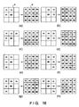
- the pattern generator 2040 performs a conversion as shown in Figs. 16(a) to 16(h) and 17(a) to 17(h).
- the number of the multivalued data, to which a reference is made is nine as shown in Fig. 14B as an alternative to 36 since the multivalued data is arranged in a unit of 150 lines.
- the conversion is performed every four clocks (LCLK) 15.
- the six memories of the seven memories have been brought to the reading mode.
- data for the six pixels for each of the lines is stored in the shift registers 2034-1 to 2034-6 so as to be subjected to the serial-to-parallel conversion.
- 54-bits data 54 bits x 6 in all
- the smoothing circuit 2035 54 bits x 6 in all
- the selector 2045 selects data on a non-conversion path 2043, while data on an output path 2044 from the pattern generator 2040 is selected by the same.
- the output becomes 1A, 1A, 1A and 1A in this sequential order as shown in Fig. 18(c) since the line address signal 2018 is "00" at this time. Since the line address signal 2018 is "01" at the second reading, the output transits to the same pixel regions transits as 1A, 1A, 6B and 6B in this sequential order. Similarly, the data is transmitted in the sequential order of 1A, 6B, 3C and 3C at the third reading, while the data is transmitted in the sequential order of 1A, 6B, 3C and 3C at the fourth reading.
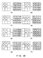
- Figs. 19(a) to 19(h) and 20(a) to 20(h) illustrates the improvements in the density patterns shown in Figs. 16(a) to 16(h) and 17(a) to 17(h). As can be clearly seen from the drawings, the outline is further smoothed.
- Figs. 19 (a), 19 (b) and 20 (c) and 20 (d) respectively show the cases where the inclination of the boundary makes 45° and 135° and a subject pixel of 150 dpi is sectioned in a proportion of 3:13.
- the boundary is 45° and 135° and the subject pixel of 150 dpi is sectioned at a proportion of 3:5.
- (c) to (f) respectively illustrate the cases where the boundary is 27°, 63°, 117° and 153° and the subject pixel of 150 dpi is sectioned into a proportion of 1:3.
- the joint between the pixels can be further smoothed.
- the boundary can be clearly expressed by performing smoothing.
- Fig. 21 is a block diagram which illustrates a portion of the printer engine portion 200 according to a fourth embodiment.
- the printer controller 100 transmits binary pixel data in the form of 300 dpi data to the printer engine portion 200.
- the multivalued pixel data is transmitted at the same timing as that for the binary pixel data to the printer engine portion 200, substantially 150 dpi data is formed by successively transmits the same pixel data two times.
- reference numeral 3001 represents a selector for writing 8 bits signal consisting of 6-bits multivalued video signals VD00 to VD05, binary video signal VIDEO (1-bit) and multivalue/binary selection signal M/B (1-bit) supplied from the printer controller 100 in synchronization with the image clock VCLK to a line memory selected from line memories 3002 to 3004.
- the line memories 3002 to 3004 are the memories each of which has a capacity of storing 8-bits video signal for one line in the main scanning direction and arranged to be read and write in accordance with the image clock signal VCLK.
- Reference numerals 3005 and 3006 represent selectors each of which selects output data from any of the line memories 3002 to 3004 so as to write it to shift registers 3008 and 3009.
- Reference numeral 3007 represents a device control circuit which controls the above-described selectors 3001, 3005 and 30006 and the line memories 3002 to 3004 in response to the beam detect signal BD which is a known synchronizing signal in the main scanning direction.
- Reference numerals 3008 and 3009 represent shift registers capable of storing six pixel data items each of which has the depth corresponding to 8 bits, pixel data stored in the respective shift outputs 1a to 1f and 2a to 2f being supplied to a determination circuit 3010.
- the determination circuit 3010 performs a predetermined processing in accordance with the supplied pixel data so that the laser drive signal LD is transmitted.
- the printer controller 100 has a binary and a multivalued bit map memories so as to transmit the binary image data developed therein as the signals VD0 to VD05 for one each line in the main scanning direction in synchronization with the signal BD.
- the data for each of the pixels is transmitted in synchronization with the image clock signal VCLK, the resolution is 150 dpi in the case where the data is multivalued data. Therefore, the controller transmits the same data for two clock pulses of the VCLK signal.
- a multivalue/binary selection signal M/B is, as a signal for selecting whether the printing is performed in accordance with either signal, transmitted in response to the VCLK signal in the case where both binary data and multivalued data exist for a certain pixel.
- the 8-bits video signal for one line in the main scanning direction is written to any of the line memories 3002 to 3004 selected by the selector 3001.
- the data which has been previously written is read from the residual two line memories except for the line memory which has been brought to the writing mode.
- the data thus read out is supplied to the selectors 3005 and 3006.
- the timing of the operation of each of the selectors and the line memories controlled by a device control circuit 3007 is shown in Fig. 22.
- symbol “Wn” represents timing at which data on the n-th line in the main scanning direction is written
- symbol “Rn” represents timing at which data on the m-th line is read
- symbols “Rm/Wn” denote a case where the reading of the m-th line and writing to the n-th line are simultaneously performed.
- data is written to the line memories 3002, 3003, 3004, 3002,..., in this sequential order.
- data reading is performed in such a manner that the same data is read two times from a pair consisting of an odd-number line and the next even-number line so as to be respectively supplied to-the shift registers 3008 and 3009.
- the shift outputs 1a to 1f and 2a to 2f from each of the shift registers 3008 and 3009 are supplied to the determination circuit 3010. That is, data for 6 pixels in the lateral direction for the neighboring two lines, that is, data for 2 x 6 pixels is latched by the shift registers 3008 and 3009.
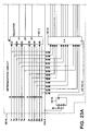
- FIG. 23A and 23B An example of the structure of the determination circuit 3010 is as shown in Figs. 23A and 23B.
- reference numeral 3011 represents a selector which selects the supplied data pair "A" or "B” as output Y.
- Reference numeral 3014 represents a selector for selecting a pair from the three input pairs A to C as the output Y.
- Reference numeral 3015 represents a pulse width modulation circuit for transmitting pulse width modulation signal PW in response to the multivalued video signals VDOO to VD05.
- Reference numerals 3020 to 3022 represent a mixture determination circuit for determining whether or not multivalued data and binary data are mixed in the pixel in a unit of 150 dpi.
- Reference numeral 3023 represents a mixing direction determination circuit for determining the direction of the multivalue/binary mixed pixel of the subject pixel when viewed at the resolution of 150 dpi.
- Reference numeral 3024 represents a signal selection circuit for transmitting selection signal PSEL and M/B′ (to be described later) serving as the printing signal in response to the above-described information about the mixture and the mixing direction signal.
- the pixel data for the odd-number line is transmitted from the shift outputs 1a to 1f of the shift register 3008, while pixel data for the even-number line is transmitted from the shift outputs 2a to 2f of the shift register 3009.
- 1d is the subject pixel
- 1c is the data for the right pixel adjacent to the subject pixel 1d when viewed at a unit of 300 dpi
- 1e is the data for the left pixel adjacent to the subject pixel 1d
- 1b is the data for the right pixel adjacent to data 1d which expresses a portion of the subject data 1d when viewed in a unit of 150 dpi
- 1f is the data for the left pixel.
- 2d is the pixel data which expresses a portion of the subject pixel when viewed in a unit of 150 dpi and other symbols hold the similar relationship for the odd-number line.
- Data 1b, 1d and 1f are supplied to the input A of the selector 3011, while 2b, 2d and 2f are supplied to the input B of the selector 3011.
- the selector 3011 alternately transmits the inputs A and B for each line in response to signal LSEL which is alternately switched in response to the signal BD by a J-K flip-flop 3017. That is, data 1b, 1d and 1f are selected/transmitted for the odd-number line, while data 2b, 2d and 2f are selected/transmitted for the even-number line.
- the output data is delayed by the D-flip-flops 3012 and 3013 by a degree corresponding to two clocks of the signal VCLK so that tha data is syncronized with data deleyed by flip-flop 3019, and is supplied to the selector 3014.
- the multivalue/binary selection signal M/B included in the input signals 1a to If and 2a to 2f is latched by signal 1/2 VCLK halved by the J-K flip-flop 3018. That is, data is latched in the flip-flop 3019 at a unit of 150 dpi.
- the signals 1c, 1d, 2c and 2d are 4-dot data which forms the subject pixel when viewed in a unit of 150 dpi. That is, 1c is the data for the upper right portion of the subject pixel, 1d is the data for the upper left portion, 2c is the data for the lower right portion and 2d is the data for the lower left portion.
- 1a, 1b, 2a and 2b are data for the dot which forms the pixel at right of the subject pixel (to be called a "right pixel” hereinafter) when viewed in a unit of 150 dpi
- 1e, 1f, 2e and 2f are data for the dot which forms the pixel at left of the subject pixel (to be called a "left pixel” hereinafter).
- the positional relationship between the pixel groups is shown in Fig. 24.
- the multivalue/binary selection signal M/B for each of the left pixel signals 1e, 1f, 2e and 2f of the output data from the flip-flop 3019 is supplied to the mixture determination circuit 3020.
- the multivalue/binary selection signal M/B of the subject pixel signals 1c, 1d, 2c and 2d are supplied to the mixture determination circuit 3021 and the mixture direction determination circuit 3023.
- the multivalue/binary selection signal M/B of the right pixel signals 1a, 1b, 2a and 2b is supplied to the mixture determination circuit 3022.
- Each of the mixture determination circuits makes a determination whether or not the multivalued pixel data and the binary pixel data are mixed in the 150 dpi pixel.
- the signal 1d-M/B, 2d-M/B, 1c-M/B and 2c-M/B of the subject pixel are supplied to the mixture direction determination circuit 3023 in which the region, in which the multivalued data exists in the subject pixel, is positioned on the right side of the subject pixel or the left side is determined.
- the mixture direction determination circuit 3023 transmits signal RIGHT if it has determined that the multivalued data is positioned on the right side of the pixel, while it transmits signal LEFT-if it has been determined that the multivalued data is positioned on the left side.
- An example of the structure of the mixture direction determination circuit 3023 is shown in Fig. 25.
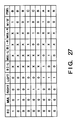
- Fig. 26 illustrates mixture patterns of the multivalue/binary data in a pixel of 150 dpi and outputs when the pixel of each of the mixture patterns has been determined by the circuit shown in Fig. 25.
- the pattern which becomes symmetric with respect to the center line in the main scanning direction of the 150 dpi pixel becomes the same result, its pattern is omitted from the illustration.
- each of the output signals from the mixture determination circuits 3020 to 3022 and the mixture direction determination circuit 3023 are supplied to the signal selection circuit 3024.
- the signal selection circuit 3024 transmits signal PSEL for selecting a pixel signal with which the printing is performed and the signal M/B′.
- the signal PSEL acts to select a signal from the left pixel signal, the subject pixel signal and the right pixel signal with which the printing is performed, the selected signal being then supplied to the selector 3014.
- the signal M/B′ selects the multivalue processing or the binary processing in response to the signal of the pixel selected in response to the signal PSEL, the signal M/B′ being supplied to a selector 3016 via an OR circuit 3025.
- the left pixel video signal is supplied to the input A of the selector 3014, the subject pixel video signal is supplied to the input B and the right pixel video signal is supplied to the input C.
- the PSEL signal selects and transmits any of the above-described pixel video signals.
- the signals PSEL and M/B′ are determined in accordance with the following algorithm.
- the M/B′ signal of level "1" is transmitted.
- the signal M/B′ of level "0" is transmitted in the other case.
- the binary signal VIDEO of the signals selected by the selector 3014 is synthesized with the clock VCLK by the flip-flop 3026 so as to be supplied to the input B of the selector 3016, while the multivalued signals VD00 to VD05 are supplied to the pulse width modulation circuit 3015.
- FIG. 28 An example of the pulse width modulation circuit 3015 is shown in Fig. 28.
- reference numeral 3801 represents a latch for latching the multivalued image data VD00 to VD05.
- Reference numeral 3802 represents an oscillator for generating predetermined period clock 16f which expresses the printing density realized by the printer apparatus in the main scanning direction, the oscillator 3802 being a synchronizing oscillator acting in synchronization with the image clock VCLK (3807).
- the synchronizing oscillator 3802 transmits the clock 16f the frequency of which is 16 times the frequency of the clock VCLK assuming that the frequency of the VCLK is f.
- Reference numeral 3803 represents a main scanning counter which performs the counting in accordance with the clock 16f supplied from the synchronizing oscillator 3802.
- Reference numeral 3804 represents a sub-scanning counter for performing the counting the number of the horizontal synchronizing BD signal 3808.
- Reference numeral 3805 represents a table memory which receives the input video signal and the output value from each of the counters 3803 and 3804 and transmits the results of "1" and "0” obtained by dither processing the multivalued input video signal by a predetermined threshold matrix.
- Reference numeral 3806a represents a video signal input terminal through which the multivalued video signals VD00 to VD05 (3806) are supplied.
- Reference numeral 3807a represents an input terminal for the image clock VCLK (3807) and 3808a represents an input terminal for the horizontal synchronizing signal BD (3808).
- Reference numeral 3809a represents an input terminal for the vertical synchronizing signal VSYNC (3809) and 3810 represents a binary signal transmitted from the table memory 3805, that is, video signal PW which has been dither-processed. Then, the operation of the above-described circuit will be described.
- the 6-bits multivalued video signals VD00 to VD05 (3806) supplied from the selector 3014 are latched by the latch circuit 3801 in accordance with the image clock VCLK (3807).
- the multivalued video signals thus latched are supplied as the address signals for the table memory 3805.
- the image clock 3807 triggers the synchronizing oscillator 3802 so that the output 16f from the synchronizing oscillator 3802 counts up the main scanning counter 3803.
- the main scanning counter 3803 expresses the counted value in the form of a parallel binary 5-bits data which is then supplied to the upper bit portion of the bit in the table memory 3805 to which the multivalued video signal 3806 has been supplied.
- the main scanning counter 3803 is reset in response to the horizontal synchronizing signal BD (3805) so as to act as a point address formed by finely sectioning the pixel region (1-dot region of 4800 dpi).
- the sub-scanning counter 3804 is counted up in response to the horizontal synchronizing signal BD (3808), the counted value being expressed by a binary 1-bit data.
- the 1-bit data is supplied to the upper bit of the bit in the table memory 3805 to which the counted value of the counter 3803 is supplied.
- the sub-scanning counter 3804 is reset at the forward end of the image region in response to the vertical synchronizing signal VSYNC (3809) so as to act as a pointer for the sub-scanning direction.
- each of the threshold values in the 32 x 2 dither matrix is selected.
- the threshold in the dither matrix has been set in accordance with the characteristics of the printer.
- the signals "1" and "0" which are the results of the comparison between the threshold in the matrix and the value of the multivalued video signal are stored in the respective addresses of the table memory 3805.
- a 300 dpi pixel can be expressed by four pixels consisting of two pixels in the main scanning direction and two pixels in the sub-scanning direction, that is, expressed in 64 gradations in a unit of 150 dpi.
- the signal PW is transmitted in the form of a signal the pulse width of which has been modulated in a unit of 1/16 of a pixel in the case of the binary processing.
- the signal PW thus processed is supplied to the input A of the selector 3016 shown in Figs. 23A and 23B.
- the selector 3016 selects the binary video signal VIDEO when the selection signal VSEL is "1" and selects the pulse width modulation signal PW which is a binary video signal when the selection signal VSEL is "0".
- the selection signal VSEL is formed by calculating the OR of the multivalue/binary selection signal M/B (the output from the flip-flop 13) about the subject pixel position and the output M/B′ from the signal selection circuit.
- a signal selected in response to the selection signal VSE1 serves as laser drive signal LD so that a semiconductor laser (omitted from illustration) is operated. As a result, the printing is performed by a known electrophotographic process.
- undesired gray portion which may be generated on the boundary when a multivalue/binary data is written in an overlapped manner at the time of the post-script processing, can be eliminated.
- an image exhibiting an excellent quality can be formed.
- the above-described algorithm is employed in the determination processing according to the fourth embodiment, the present invention is not limited to this.
- the description is made about a case in which the resolution of the printer is 300 dpi and the resolution in the case of the multivalued printing is 150 dpi.
- the present invention is not limited to this.
- the structure according to the fourth embodiment can be applied to a case in which printing is performed by a printer having a resolution of 600 dpi in such a manner that a multivalued data image is printed in the form of 150 dpi data by collecting 16 pixels of 600 dpi data.
- the structure is slightly changed, it can be easily realized by employing a structure in which the reading of the memory is performed two times into a structure in which it is performed four times.
- the processing portion is provided for the portion in the vicinity of the printer engine 200. However, it may, of course, be provided for the portion in the vicinity of the printer controller 100. Furthermore, whether or not the above-described processing is performed may be instructed with a command.
- the laser beam printer is employed in the description according to this embodiment, the present invention is not limited to this. The present invention can be applied to any of the printers capable of performing a plurality of processings having different resolutions.
- Figs. 30A and 30B are block diagram of a video signal processing portion according to a fifth embodiment of the present invention.
- the reference is made to only the two pixels disposed adjacent to each other in the main scanning direction of the subject pixel when viewed in a unit of 150 dpi.
- the reference is made to 8 pixels surrounding and positioned in contact with the pixel to be printed.
- the line memory having a capacity of substantially three times the structure shown in Fig. 21 must be provided. Specifically, for example, a structure as shown in Figs. 30A and 30B is necessary to be arranged.
- the shift outputs are supplied to a determination circuit 3122 so as to be subjected to predetermined processings.
- the determination circuit 3122 may, basically, arranged in such a manner that the processings according to the fourth embodiment of the present invention shown in Figs. 23A and 23B are performed for each of the lines in parallel. Therefore, since the structure is arranged similarly except for the number of the signals which is three times the structure shown in Fig. 3, its illustration is omitted.
- the determination circuit 3122 acts in such a manner that, when a multivalue/binary data mixture is detected in signals 3c, 3d, 4c and 4d of the 300 dpi pixel constituting the subject pixel when viewed in a unit of 150 dpi, it is replaced by data for a non-mixed pixel data for the surrounding 8 pixels.
- the detection of the 8 non-mixed pixel data is performed by the circuits similarly arranged to the mixture determination circuits 3020, 3021 and 3022 shown in Figs. 23A and 23B Since other structures are the same as those according to the fourth embodiment of the present invention, its description is omitted.
- the number of the pixels to which the reference is made is large, it might be considered feasible to employ an algorithm from a multiplicity of algorithms. A preferred one may be selected depending upon the characteristics of the printer. According to this embodiment, since the number of the pixels, to which the reference is made, becomes large, the processing can be further accurately performed.
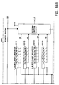
- Figs. 33A and 33B are block diagram which illustrates the structure according to a sixth embodiment of the present invention.
- the timing of the control of each of the line memories and the selectors is shown in Fig. 34.
- the region of the 150 dpi unit pixel, to which the reference is made is the same as that according to the fifth embodiment.
- the structure is characterized in that the region, to which the reference is made, is restricted for the pixels positioned in vertically and diagonally contact with the subject pixel so that the number of the line memories is reduced.
- Fig. 35 illustrates the positional relationship between the subject pixel and the pixel group to which the reference is made.
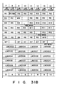
- the pixels are given the symbols as illustrated so as to represent the shift outputs from the shift registers 3212 to 3215 shown in Figs. 33A and 33B.
- the pixels adjacent to 2c, 2d, 3c and 3d constituting the subject pixel in the main scanning direction are subjected to the similar determination processing to that according to the fourth and the fifth embodiments.
- the reference is made to only two pixels of the four 300 dpi pixels constituting the pixel of 150 dpi unit in the main scanning direction, the two pixels being positioned adjacent to the pixel to be printed. That is, the upper right pixel is processed in such a manner that the reference is made to 1a and 1b and the upper pixel is processed in such a manner that the reference is made to 1c and 1d. The upper left pixel is processed in such a manner that the reference is made to 1e and 1f and the lower right pixel is processed in such a manner that the reference is made to 4a and 4b.
- the lower pixel is processed in such a manner that the reference is made to 4c and 4d and the lower left pixel is processed in such a manner that the reference is made to 4e and 4f.
- the determination of the above-described pixel, whether or not the mixture of the multivalue/binary data items exist, is made in such a manner that it is determined that it is the mixture of the binary data if the both pixels are binary data, it is the non-mixture pixel of the multivalued data if the both pixels are multivalued data and it is the mixed pixel of the multivalue/binary data in other cases.
- the mixture data for the subject pixel is replaced by the non-mixture data for the pixel, to which the reference is made, so as to perform the printing.
- the number of the necessary line memories can be reduced, and economical advantage can be obtained.
- Figs. 36A and 36B are block diagram which illustrates the structure of the seventh embodiment of the present invention.
- the multivalued data and the binary data are separated from each other at the time of writing the video signal to the line memory so as to be individually written to the respective memories.
- the line memories 3302 to 3308 serve as the line memories to which binary data is written in such a manner that the binary video signal VIDEO and the multivalue/binary selection signal M/B are written at a density of 300 dpi.
- the operation timing for each of the line memories and selectors 3309 to 3314 and the shift registers 3316 to 3321 is the same as that according to the fifth embodiment.
- the line memories 3324 to 3327 serve as the line memories to which the multivalued video signals VD00 to VD05 are written in such a manner that the writing is performed at a density of 150 dpi in accordance with the clock 1/2 VCLK obtained by halving the image clock VCLK. Furthermore, data reading from the above-described line memories is performed two times so as to be supplied to the shift registers 3331 to 3333 which also shift the supplied signals in accordance with the clock 1/2 VCLK so as to transmit each of the shifted signals. The shift output from each of the shift registers 3316 to 3321 and 3331 to 3333 is supplied to a determination circuit 3322 so as to be subjected to the processings similar to those according to the second embodiment. As a result, the printing is performed.
- the seventh embodiment since the binary signal and the multivalued signal are separated from each other and the binary signal is written to the line memory at the density of 300 dpi and the multivalued signal having a large number of bits is written to the same at the density Of 150 dpi, the necessary memory capacity can be reduced in addition to the effect obtained from the fourth embodiment.
Landscapes
- Engineering & Computer Science (AREA)
- Physics & Mathematics (AREA)
- General Physics & Mathematics (AREA)
- Theoretical Computer Science (AREA)
- Multimedia (AREA)
- Signal Processing (AREA)
- General Engineering & Computer Science (AREA)
- Facsimile Image Signal Circuits (AREA)
- Color, Gradation (AREA)
- Image Processing (AREA)
- Editing Of Facsimile Originals (AREA)
Claims (15)
- Bildverarbeitungsgerät (53) mit:
einer Eingabeeinrichtung zur Eingabe mehrwertiger Daten (VDO), die Pixel darstellen und eine erste Auflösung haben; und
einer Einrichtung (10, 17) zur Umwandlung der Eingabedaten in mehrwertige Daten (VDO′), die eine zweite Auflösung höher als die erste Auflösung haben; und
gekennzeichnet dadurch,
daß die Umwandlungseinrichtung eine Einrichtung zum Vergleich des Unterschieds zwischen Eingabedaten, die zwei benachbarte Pixel darstellen mit einem vorbestimmten Wert (T) enthält;
daß die Umwandlungseinrichtung eingerichtet ist zur Umwandlung von Eingabedaten in mehrwertige Daten der zweiten Auflösung, in Übereinstimmung damit, ob der Unterschied zwischen den mehrwertigen Eingabedaten größer ist als der vorbestimmte Wert oder nicht. - Gerät nach Anspruch 1, wobei die Umwandlungseinrichtung wiederholt die mehrwertigen Eingabedaten ausgibt wenn der Unterschied größer ist als der vorbestimmte Wert und mindestens einen Mittelwert erzeugt, der gewichtet ist nach den benachbarten Pixeldaten, wenn der Unterschied nicht größer ist als der vorbestimmte Wert.
- Gerät nach Anspruch 2, wobei die Umwandlungseinrichtung außerdem enthält:
eine Einrichtung (17) zur Umwandlung der Eingabedaten in eine erste Richtung; und
eine Einrichtung (10) zur Umwandlung der in die erste Richtung umgewandelten mehrwertigen Daten in eine zweite Richtung. - Gerät nach einem der vorstehenden Ansprüche mit: einer Einrichtung (35) zur Erzeugung eines pulsweiten-modulierten Signals, das in Übereinstimmung mit den mehrwertigen Daten die die zweite Auflösung haben moduliert ist.
- Gerät nach Anspruch 4, mit: einer Aufzeichnungseinrichtung (200) zur Aufzeichnung eines Bildes in Übereinstimmung mit dem pulsweiten-modulierten Signal.
- Gerät nach Anspruch 5, wobei die Aufzeichnungseinrichtung ein erstes horizontales Synchronisierungssignal erzeugt, und wobei das Gerät eine Einrichtung für die Erzeugung eines zweiten horizontalen Synchronisierungssignals in Reaktion auf eine Vielzahl des ersten horizontalen Synchronisierungssignals enthält.
- Gerät nach Anspruch 5, wobei die Aufzeichnungseinrichtung ein Bild unter Verwendung eines elektrostatischen Aufzeichnungsverfahrens auf ein Aufzeichnungsmedium aufzeichnet.
- Gerät nach Anspruch 5, wobei die Aufzeichnungseinrichtung ein Bild unter Verwendung eines elektrophotographischen Verfahrens mit Laser auf ein Aufzeichnungsmedium aufzeichnet.
- Verfahren zur Verarbeitung von Bilddaten mit Eingabe von mehrwertigen Bilddaten (VDO), die Pixel darstellen und eine erste Auflösung haben, außerdem die Umwandlung (10, 17) von Eingabedaten in mehrwertige Daten (VDO′) mit einer zweiten Auflösung, höher als die erste einschließen;
gekennzeichnet dadurch,
daß in der Umwandlung der Unterschied zwischen Eingabedaten, die zwei benachbarte Pixel darstellen, mit einem vorbestimmten Wert (T) verglichen wird, und die Eingabedaten in mehrwertige Daten der zweiten Auflösung umgewandelt werden in Übereinstimmung damit, ob der Unterschied zwischen den mehrwertigen Eingabedaten größer ist als der vorbestimmte Wert oder nicht. - Verfahren nach Anspruch 9, währenddessen die Umwandlungseinrichtung (10, 17) wiederholt die mehrwertigen Eingabedaten ausgibt, wenn der Unterschied größer ist als der vorbestimmte Wert und mindestens einen Mittelwert, gewichtet nach den benachbarten Pixeldaten, erzeugt, wenn der Unterschied nicht größer ist als der vorbestimmte Wert.
- Verfahren nach Anspruch 9 oder 10, in dem die Eingabedaten in eine erste Richtung umgewandelt werden und die umgewandelten Daten dann in eine zweite Richtung umgewandelt werden.
- Verfahren nach jedem der Ansprüche 9 bis 11, in dem die umgewandelten Daten zur Erzeugung (35) eines pulsweiten-modulierten Signals verwendet werden.
- Verfahren nach Anspruch 12, wobei das pulsweiten-modulierte Signal die Aufzeichnungseinrichtung (200) ansteuert.
- Verfahren nach Anspruch 13, wobei die Aufzeichnungseinrichtung ein Bild unter Verwendung eines elektrostatischen Aufzeichnungsverfahrens auf ein Aufzeichnungsmedium aufzeichnet.
- Verfahren nach Anspruch 13, wobei die Aufzeichnungseinrichtung ein Bild unter Verwendung eines elektrophotographischen Verfahrens und eines Lasers auf ein Aufzeichnungsmedium aufzeichnet.
Applications Claiming Priority (6)
| Application Number | Priority Date | Filing Date | Title |
|---|---|---|---|
| JP1229120A JP3039662B2 (ja) | 1989-09-06 | 1989-09-06 | 記録装置 |
| JP229120/89 | 1989-09-06 | ||
| JP2001006A JPH03207164A (ja) | 1990-01-09 | 1990-01-09 | 画像記録装置 |
| JP1006/90 | 1990-01-09 | ||
| JP16100/90 | 1990-01-29 | ||
| JP1610090A JPH03221475A (ja) | 1990-01-29 | 1990-01-29 | 記録装置 |
Publications (3)
| Publication Number | Publication Date |
|---|---|
| EP0416886A2 EP0416886A2 (de) | 1991-03-13 |
| EP0416886A3 EP0416886A3 (en) | 1992-02-05 |
| EP0416886B1 true EP0416886B1 (de) | 1995-04-19 |
Family
ID=27274715
Family Applications (1)
| Application Number | Title | Priority Date | Filing Date |
|---|---|---|---|
| EP90309691A Expired - Lifetime EP0416886B1 (de) | 1989-09-06 | 1990-09-05 | Bildaufzeichnungsgerät |
Country Status (3)
| Country | Link |
|---|---|
| US (3) | US5850295A (de) |
| EP (1) | EP0416886B1 (de) |
| DE (1) | DE69018739T2 (de) |
Families Citing this family (14)
| Publication number | Priority date | Publication date | Assignee | Title |
|---|---|---|---|---|
| US5185852A (en) * | 1991-05-31 | 1993-02-09 | Digital Equipment Corporation | Antialiasing apparatus and method for computer printers |
| JP2804187B2 (ja) * | 1991-07-05 | 1998-09-24 | 沖電気工業株式会社 | ノンインパクトプリンタ |
| JP3634940B2 (ja) * | 1997-05-12 | 2005-03-30 | 株式会社日立製作所 | 画像記録装置 |
| US6304337B1 (en) | 1998-12-21 | 2001-10-16 | Lexmark International, Inc. | Stochastic method of enlarging a visual image |
| US6115031A (en) * | 1999-04-23 | 2000-09-05 | Lexmark International, Inc. | Method of converting color values |
| US6295078B1 (en) * | 1999-05-26 | 2001-09-25 | Hewlett-Packard Company | Methods of providing lower resolution format data into a higher resolution format |
| US6707578B1 (en) * | 1999-09-20 | 2004-03-16 | Hewlett-Packard Development Company, L.P. | Method and apparatus for improving image presentation in a digital copier |
| JP4916059B2 (ja) * | 2001-07-31 | 2012-04-11 | キヤノン株式会社 | 画像処理装置 |
| US7872775B2 (en) | 2002-05-24 | 2011-01-18 | Lexmark International, Inc. | Apparatus and method for a resolution quality redefinition control system for a multi-function device |
| JP2005001136A (ja) * | 2003-06-09 | 2005-01-06 | Noritsu Koki Co Ltd | 露光装置及び露光方法 |
| US7529423B2 (en) * | 2004-03-26 | 2009-05-05 | Intel Corporation | SIMD four-pixel average instruction for imaging and video applications |
| US8787690B2 (en) | 2008-11-12 | 2014-07-22 | Abbyy Development Llc | Binarizing an image |
| US8098945B2 (en) * | 2008-11-12 | 2012-01-17 | Abbyy Software Ltd. | Method and system for binarizing an image |
| JP7428041B2 (ja) * | 2020-03-25 | 2024-02-06 | 京セラドキュメントソリューションズ株式会社 | 液面検知装置及び画像形成装置 |
Family Cites Families (39)
| Publication number | Priority date | Publication date | Assignee | Title |
|---|---|---|---|---|
| US4506301A (en) * | 1979-10-12 | 1985-03-19 | Xerox Corporation | Multiple mode raster scanner |
| US4400738A (en) * | 1981-10-30 | 1983-08-23 | Xerox Corporation | Image signal processing method and apparatus |
| JPS5963864A (ja) * | 1982-10-05 | 1984-04-11 | Canon Inc | 画像処理装置 |
| US4658300A (en) * | 1983-03-08 | 1987-04-14 | Canon Kabushiki Kaisha | System and method for processing image signals |
| JPS59163953A (ja) * | 1983-03-08 | 1984-09-17 | Canon Inc | 画像処理装置 |
| US4709274A (en) * | 1983-08-29 | 1987-11-24 | Canon Kabushiki Kaisha | Image processing apparatus |
| JPH0620244B2 (ja) * | 1983-11-18 | 1994-03-16 | 株式会社リコー | 通信端末装置 |
| JPS60218181A (ja) * | 1984-04-13 | 1985-10-31 | Fujitsu Ltd | 画像処理装置 |
| US4712185A (en) * | 1984-04-28 | 1987-12-08 | Kabushiki Kaisha Toshiba | Dot interpolation control system |
| JPS6110360A (ja) * | 1984-06-26 | 1986-01-17 | Canon Inc | 画像処理装置 |
| US4631751A (en) * | 1984-10-24 | 1986-12-23 | Anderson Karen L | Method for enlarging a binary image |
| US4885786A (en) * | 1984-10-24 | 1989-12-05 | International Business Machines Corporation | Method for enlarging an image stored in run representation form |
| US4578689A (en) * | 1984-11-26 | 1986-03-25 | Data Recording Systems, Inc. | Dual mode laser printer |
| JPH0659106B2 (ja) * | 1985-03-04 | 1994-08-03 | 凸版印刷株式会社 | ビデオ画像処理装置 |
| JPS61230571A (ja) * | 1985-04-05 | 1986-10-14 | Dainippon Screen Mfg Co Ltd | 画像走査装置 |
| DE3789461D1 (de) * | 1986-01-22 | 1994-05-05 | Konishiroku Photo Ind | Bildverarbeitungssystem mit Fähigkeit zum Vergrössungs- und Reduzier-Betrieb. |
| US4906675A (en) * | 1986-02-12 | 1990-03-06 | Mitsui Petrochemical Industries, Ltd. | Active energy ray-curable composition |
| US4831392A (en) * | 1986-02-13 | 1989-05-16 | Canon Kabushiki Kaisha | Image processing apparatus using pulse width modulation with improved sensitivity |
| US4841375A (en) * | 1986-05-29 | 1989-06-20 | Kabushiki Kaisha Toshiba | Image-resolution conversion apparatus for converting a pixel-density of image data |
| US5175635A (en) * | 1986-06-02 | 1992-12-29 | Kabushiki Kaisha Toshiba | Picture printing apparatus using multivalued patterns, binary patterns and dither patterns selectively |
| JPS6312019A (ja) * | 1986-07-02 | 1988-01-19 | Graphtec Corp | ビデオプリンタ |
| EP0506148B1 (de) * | 1986-08-29 | 1999-10-27 | Canon Kabushiki Kaisha | Ein-/Ausgabegerät und Verfahren zur Verarbeitung von Bilddaten |
| US4905097A (en) * | 1986-09-20 | 1990-02-27 | Canon Kabushiki Kaisha | Image processing system capable of processing both binary and multivalue image data and having converters for converting each type of image data into the other type of image data |
| JP2508512B2 (ja) * | 1986-10-17 | 1996-06-19 | ソニー株式会社 | 映像信号処理装置 |
| US4930087A (en) * | 1987-08-10 | 1990-05-29 | Kabushiki Kaisha Toshiba | Image forming apparatus |
| US5163122A (en) * | 1987-12-09 | 1992-11-10 | Fuji Photo Film Co., Ltd. | Image processing system |
| GB8814288D0 (en) * | 1988-06-16 | 1988-07-20 | Crosfield Electronics Ltd | Method & apparatus for generating composite images |
| EP0356224B1 (de) * | 1988-08-25 | 1996-12-11 | Canon Kabushiki Kaisha | Datenverarbeitungsgerät |
| US5045869A (en) * | 1988-09-16 | 1991-09-03 | Canon Kabushiki Kaisha | Printing controller for printing at selected resolutions |
| JP3018337B2 (ja) * | 1988-09-17 | 2000-03-13 | ブラザー工業株式会社 | 画像処理装置 |
| DE69030746T2 (de) * | 1989-03-15 | 1997-10-23 | Canon Kk | Ausgabevorrichtung |
| US5008752A (en) * | 1989-06-16 | 1991-04-16 | Eastman Kodak Company | Digital image interpolator with multiple interpolation algorithms |
| US5129048A (en) * | 1989-07-31 | 1992-07-07 | Eastman Kodak Company | Efficient data storage system for gray-scale printers |
| US4975785A (en) * | 1989-08-04 | 1990-12-04 | International Business Machines Corporation | Pel resolution addressing conversion |
| DE69027723T2 (de) * | 1989-09-07 | 1997-01-09 | Canon Kk | Bilddarstellungsgerät |
| US5025325A (en) * | 1989-10-13 | 1991-06-18 | Hewlett-Packard Company | Graphics scaling method for high resolution printers |
| DE69126457T2 (de) * | 1990-03-02 | 1997-11-06 | Canon Kk | Bildverarbeitungsvorrichtung |
| US5337167A (en) * | 1991-04-03 | 1994-08-09 | Matsushita Electric Industrial Co., Ltd. | Halftone image forming apparatus including density based dot enlargement |
| US5270837A (en) * | 1991-09-27 | 1993-12-14 | Apple Computer, Inc. | Method and apparatus for enabling intelligent post-processing of differing data types |
-
1990
- 1990-09-05 DE DE69018739T patent/DE69018739T2/de not_active Expired - Fee Related
- 1990-09-05 EP EP90309691A patent/EP0416886B1/de not_active Expired - Lifetime
-
1994
- 1994-07-15 US US08/275,254 patent/US5850295A/en not_active Expired - Fee Related
- 1994-08-15 US US08/290,078 patent/US5819010A/en not_active Expired - Fee Related
-
1995
- 1995-06-07 US US08/473,358 patent/US5729358A/en not_active Expired - Fee Related
Also Published As
| Publication number | Publication date |
|---|---|
| EP0416886A3 (en) | 1992-02-05 |
| EP0416886A2 (de) | 1991-03-13 |
| DE69018739T2 (de) | 1995-09-14 |
| US5729358A (en) | 1998-03-17 |
| US5819010A (en) | 1998-10-06 |
| DE69018739D1 (de) | 1995-05-24 |
| US5850295A (en) | 1998-12-15 |
Similar Documents
| Publication | Publication Date | Title |
|---|---|---|
| KR0156956B1 (ko) | 화상 형성 장치 및 그 방법 | |
| EP0416886B1 (de) | Bildaufzeichnungsgerät | |
| US5729663A (en) | Method and apparatus for gray screening | |
| US6332666B1 (en) | Printing apparatus, resolution conversion printing method for printing apparatus, and storage medium storing computer-readable program | |
| KR950006621B1 (ko) | 화상처리장치 | |
| US5760811A (en) | Halftone image recording apparatus and method based on first and second timing signals chosen from a plurality of synchronized clocks | |
| US5754188A (en) | Data processing apparatus | |
| EP0555064B1 (de) | Bildverarbeitungs- und Bildaufzeichnungsgerät | |
| US5327258A (en) | Image processing apparatus | |
| EP0454088B1 (de) | Bildverarbeitungsvorrichtung | |
| EP0488118B1 (de) | Abbildungsaufzeichnungsvorrichtung für Bilder hoher Qualität | |
| JP2647917B2 (ja) | 画像処理装置 | |
| JP3039662B2 (ja) | 記録装置 | |
| JP2003054032A (ja) | 印刷制御装置及びそれを有する印刷装置及び制御方法 | |
| JPH07250246A (ja) | 画像形成装置 | |
| JPH0730746A (ja) | 画像処理装置 | |
| JPH02155760A (ja) | 画像形成装置 | |
| JP4127675B2 (ja) | 画像処理装置 | |
| JPH03207164A (ja) | 画像記録装置 | |
| JPH1079856A (ja) | 画像処理装置及びその方法 | |
| JPH0922455A (ja) | 画像処理装置およびその方法 | |
| JP2020195004A (ja) | 画像形成装置とその制御方法、及びプログラム | |
| JPH1127530A (ja) | 画像処理装置および方法並びに記憶媒体 | |
| JPH10191042A (ja) | 画像処理方法及びその装置 | |
| JPH04238460A (ja) | 記録装置 |
Legal Events
| Date | Code | Title | Description |
|---|---|---|---|
| PUAI | Public reference made under article 153(3) epc to a published international application that has entered the european phase |
Free format text: ORIGINAL CODE: 0009012 |
|
| 17P | Request for examination filed |
Effective date: 19901231 |
|
| AK | Designated contracting states |
Kind code of ref document: A2 Designated state(s): DE FR GB IT |
|
| PUAL | Search report despatched |
Free format text: ORIGINAL CODE: 0009013 |
|
| AK | Designated contracting states |
Kind code of ref document: A3 Designated state(s): DE FR GB IT |
|
| 17Q | First examination report despatched |
Effective date: 19930401 |
|
| GRAA | (expected) grant |
Free format text: ORIGINAL CODE: 0009210 |
|
| AK | Designated contracting states |
Kind code of ref document: B1 Designated state(s): DE FR GB IT |
|
| REF | Corresponds to: |
Ref document number: 69018739 Country of ref document: DE Date of ref document: 19950524 |
|
| ITF | It: translation for a ep patent filed | ||
| ET | Fr: translation filed | ||
| REG | Reference to a national code |
Ref country code: GB Ref legal event code: 711B |
|
| RIN2 | Information on inventor provided after grant (corrected) |
Free format text: UCHIYAMA, SEIJI * KASHIHARA, ATSUSHI * SETO, KAORU * MANO, HIROSHI * SAITO, TETSUO * KAWANA, TAKASHI |
|
| REG | Reference to a national code |
Ref country code: GB Ref legal event code: 711H Ref country code: GB Ref legal event code: 711G Ref country code: GB Ref legal event code: 711E |
|
| PLBE | No opposition filed within time limit |
Free format text: ORIGINAL CODE: 0009261 |
|
| STAA | Information on the status of an ep patent application or granted ep patent |
Free format text: STATUS: NO OPPOSITION FILED WITHIN TIME LIMIT |
|
| 26N | No opposition filed | ||
| REG | Reference to a national code |
Ref country code: GB Ref legal event code: IF02 |
|
| PGFP | Annual fee paid to national office [announced via postgrant information from national office to epo] |
Ref country code: DE Payment date: 20041124 Year of fee payment: 15 |
|
| PGFP | Annual fee paid to national office [announced via postgrant information from national office to epo] |
Ref country code: GB Payment date: 20050822 Year of fee payment: 16 |
|
| PGFP | Annual fee paid to national office [announced via postgrant information from national office to epo] |
Ref country code: FR Payment date: 20050914 Year of fee payment: 16 |
|
| PG25 | Lapsed in a contracting state [announced via postgrant information from national office to epo] |
Ref country code: DE Free format text: LAPSE BECAUSE OF NON-PAYMENT OF DUE FEES Effective date: 20060401 |
|
| PGFP | Annual fee paid to national office [announced via postgrant information from national office to epo] |
Ref country code: IT Payment date: 20060930 Year of fee payment: 17 |
|
| GBPC | Gb: european patent ceased through non-payment of renewal fee |
Effective date: 20060905 |
|
| REG | Reference to a national code |
Ref country code: FR Ref legal event code: ST Effective date: 20070531 |
|
| PG25 | Lapsed in a contracting state [announced via postgrant information from national office to epo] |
Ref country code: GB Free format text: LAPSE BECAUSE OF NON-PAYMENT OF DUE FEES Effective date: 20060905 |
|
| PG25 | Lapsed in a contracting state [announced via postgrant information from national office to epo] |
Ref country code: FR Free format text: LAPSE BECAUSE OF NON-PAYMENT OF DUE FEES Effective date: 20061002 |
|
| PG25 | Lapsed in a contracting state [announced via postgrant information from national office to epo] |
Ref country code: IT Free format text: LAPSE BECAUSE OF NON-PAYMENT OF DUE FEES Effective date: 20070905 |