EP0417547A2 - Dispositif pour l'acquisition exacte des limites d'un interval de temps relatif à une horloge de référence - Google Patents
Dispositif pour l'acquisition exacte des limites d'un interval de temps relatif à une horloge de référence Download PDFInfo
- Publication number
- EP0417547A2 EP0417547A2 EP90116588A EP90116588A EP0417547A2 EP 0417547 A2 EP0417547 A2 EP 0417547A2 EP 90116588 A EP90116588 A EP 90116588A EP 90116588 A EP90116588 A EP 90116588A EP 0417547 A2 EP0417547 A2 EP 0417547A2
- Authority
- EP
- European Patent Office
- Prior art keywords
- current
- clock
- comparator
- latch
- arrangement according
- Prior art date
- Legal status (The legal status is an assumption and is not a legal conclusion. Google has not performed a legal analysis and makes no representation as to the accuracy of the status listed.)
- Granted
Links
- 239000003990 capacitor Substances 0.000 claims description 9
- 238000011156 evaluation Methods 0.000 claims description 6
- 230000000295 complement effect Effects 0.000 claims description 3
- 230000001934 delay Effects 0.000 claims description 3
- 230000008014 freezing Effects 0.000 claims description 3
- 238000007710 freezing Methods 0.000 claims description 3
- 230000003111 delayed effect Effects 0.000 claims 1
- 238000001514 detection method Methods 0.000 claims 1
- 238000005259 measurement Methods 0.000 description 6
- 230000008859 change Effects 0.000 description 4
- 238000005516 engineering process Methods 0.000 description 3
- 238000006243 chemical reaction Methods 0.000 description 2
- 238000011161 development Methods 0.000 description 2
- 230000018109 developmental process Effects 0.000 description 2
- 230000000694 effects Effects 0.000 description 2
- 230000006872 improvement Effects 0.000 description 2
- 238000012545 processing Methods 0.000 description 2
- 230000001360 synchronised effect Effects 0.000 description 2
- 238000005352 clarification Methods 0.000 description 1
- 238000010276 construction Methods 0.000 description 1
- 238000010586 diagram Methods 0.000 description 1
- 230000010354 integration Effects 0.000 description 1
- 238000000034 method Methods 0.000 description 1
- 230000003071 parasitic effect Effects 0.000 description 1
- 230000009467 reduction Effects 0.000 description 1
- 239000004065 semiconductor Substances 0.000 description 1
- 230000002123 temporal effect Effects 0.000 description 1
- 230000007704 transition Effects 0.000 description 1
- 238000002604 ultrasonography Methods 0.000 description 1
Images


Classifications
-
- G—PHYSICS
- G04—HOROLOGY
- G04F—TIME-INTERVAL MEASURING
- G04F10/00—Apparatus for measuring unknown time intervals by electric means
- G04F10/10—Apparatus for measuring unknown time intervals by electric means by measuring electric or magnetic quantities changing in proportion to time
-
- G—PHYSICS
- G04—HOROLOGY
- G04F—TIME-INTERVAL MEASURING
- G04F10/00—Apparatus for measuring unknown time intervals by electric means
- G04F10/04—Apparatus for measuring unknown time intervals by electric means by counting pulses or half-cycles of an AC
Definitions
- Integrating digital-to-analog converters are widespread (e.g. in digital voltmeters).
- a capacitor is first charged for a constant time with a current proportional to the analog value to be measured. Then it is discharged again with a constant current to the initial value. The time required for this is the measure for the analog value.
- Another example is the measurement of the transit time that an ultrasound pulse takes to get from the emission level of the transmitter to the receiving level of the receiver.
- metastable flip-flop states are possible. These must be prevented using suitable aids. Metastable conditions and their causes as well as measures to reduce the probability of their occurrence in the construction of an edge-controlled flip-flop are described in the German patent application P 37 31 294.4.
- a low-pass filter 5 and a Schmitt trigger 6 are therefore arranged between the AND gate 1 and the frequency divider 4. This solves the problem, but the clock frequency must inevitably be much lower than that theoretically possible by the AND gates 1 and flip-flops CL1 to CL4 used.
- the circuit according to FIG. 3 shows a digital alternative in which the signal for the time interval before the AND gate is synchronized with the inverted clock by means of an auxiliary flip-flop 7.
- the clock frequency is to be chosen so low that possible metastable states of the auxiliary flip-flop 7 have decayed in the inactive clock phase.
- the circuit according to FIG. 4 can bring about a possible improvement.
- a current-state-controlled bistable multivibrator instead of the AND gate, a current-state-controlled bistable multivibrator, a so-called transparent current latch 9, serves as a switch for the clock.
- This is followed by low pass 5 and Schmitt trigger 6 again in order to screen out possible metastable vibrations of the latch 9.
- the state of the clock (“0" or "1") is also recorded and the time resolution of the measurement is approximately doubled.
- the usable clock frequency must be significantly lower than that which the latch 9 could switch.
- the object of the invention is: - capture the end of the time interval (and possibly also the start of it) as precisely as possible, - to make the theoretically possible clock frequency fully usable despite the necessary consideration of excluding the influence of metastable states, - After the end of the time interval to save a measure of the current phase situation of the clock and not only a digital ("0" or "1"), but also the analog component of the time interval in a "0" or "1" period to capture.
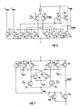
- Current-voltage converters 12, 13, 14 generate the voltage levels necessary for the logical further processing.
- a clock driver generates the clock signals in phase opposition.
- the necessary data manipulations are carried out without going through voltage levels, the generation of which takes up valuable time because of the stray capacities that are always present.
- the current cycle state is frozen in the current range with the aid of minimal voltage levels.
- the mixer monitors the correspondence of the clock phases at the outputs of the current latch 9 already in the current range with the clock phases at the input.
- the circuit principle of the comparator 8 is shown in FIG. 6. It consists of a conventional PNP transistor differential stage T1, T2 with the signal input “Event” and the reference input “U ref ", the outputs of which are loaded by NPN multiple current mirrors. These, in turn, provide the required current outputs.
- a complementary pair T5, T11 together with the current mirror T12, T13 form a current-voltage converter and provide a voltage output signal "KOMP".
- T4 supplies the currents I clock and I latch for supplying the current latch 9
- a single output T3 supplies the analog fine evaluation with the current I ramp
- a further pair of transistors T6, T9 effect a positive feedback, which is in the switching range of Comparator 8 provides an infinitely large gain (especially without hysteresis) and ensures that each output current starts immediately with 50% of its end value or switches off immediately below 50%.
- Fig. 7 shows the basic circuit structure of the current latch 9.
- the latch function is similar to that in a circuit shown in the book “Semiconductor Circuit Technology” by Tietze and Schenk, 1989, page 776, with complementary voltage outputs, but with transistors connected as diodes instead of the load resistors that form the voltage outputs in the known example, control several current outputs.
- the clock is at the inputs of a first transistor differential stage T14 and T15 in the form of the components CL1 and CL2 in phase opposition and, as long as I clock flows and I latch does not, causes the current outputs I mix 1 at T19 and I mix 2 at T20. Further current outputs of the transistors T18 and T21 following the clock generate a single-phase voltage output via the current-voltage conversion with the current mirror from the transistors T23 and T24, which, for example, can directly drive a frequency divider. The latch is therefore switched to pass (transparent).
- the second transistor differential stage T16 and T17 becomes active, introduces it (still) existing clock phase position by comparing the minimum voltage difference across the transistors connected as diodes and reinforces this tendency through the positive feedback caused by their cross-coupled outputs.
- the current clock phase state is thus "frozen", the latch is closed.
- the current latch therefore functions in the current range and the result is initially flowing or frozen currents. Only very small voltage changes occur and extremely small delays in the logical operation due to parasitic capacitances.
- the current state corresponding to the input clock or recorded is made evaluable by a current-voltage conversion, the switching delays due to technical reasons becoming fully effective again. This is not a disadvantage, because data manipulation has followed long before.
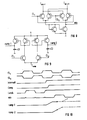
- the low-pass function described in FIG. 4 is advantageously realized.
- a Schmitt trigger is not necessary because the slope steepness already corresponds to the usual in the chosen technique.
- the criterion is the first change of clock phase after freezing the clock in the latch, ie the deviation of the clock manipulated in the latch from the original clock.
- the first clock phase change is determined with the aid of a mixer (FIG. 8); the fact of freezing is known to the comparator 8.
- the AND combination of the signals KOMP and MIX thus provides the above criterion.
- the capacitor voltage is expediently evaluated by back-integration with a constant current and measuring the time with a similar arrangement and a frequency divider or the same arrangement together with a multiplexer.
- the previous considerations essentially relate to the determination of the end of a time interval. With similar means, it is also possible to store and evaluate the instantaneous phase situation of the clock at the beginning when the interval is not synchronized, but the circuitry effort can double.
Landscapes
- Physics & Mathematics (AREA)
- General Physics & Mathematics (AREA)
- Engineering & Computer Science (AREA)
- Power Engineering (AREA)
- Measurement Of Unknown Time Intervals (AREA)
- Electric Clocks (AREA)
- Analogue/Digital Conversion (AREA)
Priority Applications (1)
| Application Number | Priority Date | Filing Date | Title |
|---|---|---|---|
| AT90116588T ATE88027T1 (de) | 1989-09-11 | 1990-08-29 | Anordnung zur genauen elektronischen erfassung der grenzen eines zeitintervalls in bezug auf einen referenztakt. |
Applications Claiming Priority (2)
| Application Number | Priority Date | Filing Date | Title |
|---|---|---|---|
| DE3930333 | 1989-09-11 | ||
| DE3930333 | 1989-09-11 |
Publications (3)
| Publication Number | Publication Date |
|---|---|
| EP0417547A2 true EP0417547A2 (fr) | 1991-03-20 |
| EP0417547A3 EP0417547A3 (en) | 1991-05-29 |
| EP0417547B1 EP0417547B1 (fr) | 1993-04-07 |
Family
ID=6389189
Family Applications (1)
| Application Number | Title | Priority Date | Filing Date |
|---|---|---|---|
| EP90116588A Expired - Lifetime EP0417547B1 (fr) | 1989-09-11 | 1990-08-29 | Dispositif pour l'acquisition exacte des limites d'un interval de temps relatif à une horloge de référence |
Country Status (5)
| Country | Link |
|---|---|
| EP (1) | EP0417547B1 (fr) |
| JP (1) | JPH03100488A (fr) |
| AT (1) | ATE88027T1 (fr) |
| CA (1) | CA2024878A1 (fr) |
| DE (1) | DE59001166D1 (fr) |
Family Cites Families (3)
| Publication number | Priority date | Publication date | Assignee | Title |
|---|---|---|---|---|
| FR1520487A (fr) * | 1967-01-24 | 1968-04-12 | Onera (Off Nat Aerospatiale) | Procédé et appareil de chronométrie |
| US4598375A (en) * | 1983-04-22 | 1986-07-01 | Hagiwara Denki Kabushiki Kaisha | Time measuring circuit |
| DE3612686A1 (de) * | 1986-04-15 | 1987-10-22 | Nukem Gmbh | Verfahren und vorrichtung zur messung von zeitintervallen |
-
1990
- 1990-08-29 AT AT90116588T patent/ATE88027T1/de not_active IP Right Cessation
- 1990-08-29 DE DE9090116588T patent/DE59001166D1/de not_active Expired - Fee Related
- 1990-08-29 EP EP90116588A patent/EP0417547B1/fr not_active Expired - Lifetime
- 1990-09-07 CA CA002024878A patent/CA2024878A1/fr not_active Abandoned
- 1990-09-07 JP JP2238809A patent/JPH03100488A/ja active Pending
Also Published As
| Publication number | Publication date |
|---|---|
| EP0417547B1 (fr) | 1993-04-07 |
| EP0417547A3 (en) | 1991-05-29 |
| CA2024878A1 (fr) | 1991-03-12 |
| DE59001166D1 (de) | 1993-05-13 |
| JPH03100488A (ja) | 1991-04-25 |
| ATE88027T1 (de) | 1993-04-15 |
Similar Documents
| Publication | Publication Date | Title |
|---|---|---|
| DE10149929B4 (de) | A/D-Wandler | |
| DE19704782C2 (de) | Magnetfelddetektor und Verfahren zum Erkennen eines Magnetfeldes | |
| EP0412618B1 (fr) | Dispositif de mesure adaptive de vitesse de rotation | |
| DE2616678B2 (de) | Oszillatorschaltung | |
| EP0316616A2 (fr) | Convertisseur analogique-numérique | |
| DE2548746A1 (de) | Analog/digital-umsetzer | |
| DE2923026A1 (de) | Verfahren und anordnung zur analog/digital-umsetzung | |
| EP0137948A1 (fr) | Dispositif pour contrôler la distance temporelle entre des signaux rectangulaires | |
| DE2952156C2 (fr) | ||
| EP0356438B1 (fr) | Procede et dispositif pour evaluer une grandeur electrique analogique | |
| DE19524387C1 (de) | Schaltungsanordnung und Verfahren zum Messen eines Kapazitätsunterschiedes zwischen einer ersten Kapazität C1 und einer zweiten Kapazität C2 | |
| DE4237196C1 (de) | Verfahren und Anordnung zur Messung zumindest einer Kapazität | |
| EP0898368B1 (fr) | Dispositif capteur | |
| CH700376A2 (de) | Kapazitiver Sensor und Verfahren zur kapazitiven Erfassung eines Objektabstandes. | |
| EP0417547B1 (fr) | Dispositif pour l'acquisition exacte des limites d'un interval de temps relatif à une horloge de référence | |
| DE3539556A1 (de) | Schaltungsanordnung zur erzeugung eines der frequenz eines wechselstromsignals zugeordneten gleichspannungsnutzsignals, insbesondere fuer die gleichlaufregelung eines elektromotors | |
| DE69204214T2 (de) | Vorrichtung zur Messung einer Drehgeschwindigkeit. | |
| DE102008042765A1 (de) | Vorrichtung und Verfahren zum Messen eines Widerstandswerts | |
| DE3814813C1 (en) | Method and circuit arrangement for analog/digital conversion | |
| DE3524530A1 (de) | Auswerteelektronik fuer differenzialwiderstaende zur verwendung in sensoren | |
| EP0360885A1 (fr) | Méthode pour la modification du rapport signal/bruit de capteurs de proximité et dispositif pour la mise en oeuvre de cette méthode | |
| EP0018349B1 (fr) | Circuit électrique pour conversion d'un courant en des impulsions, dont la durée, la période de répétition ou la fréquence correspond à l'amplitude du courant | |
| DE2521019A1 (de) | Analog/digitalkonverter | |
| DE68909609T2 (de) | Zufuhrkreis für referenzspannung. | |
| DE112021004794T5 (de) | Oszillatorschaltungsanordnung |
Legal Events
| Date | Code | Title | Description |
|---|---|---|---|
| PUAI | Public reference made under article 153(3) epc to a published international application that has entered the european phase |
Free format text: ORIGINAL CODE: 0009012 |
|
| 17P | Request for examination filed |
Effective date: 19901205 |
|
| AK | Designated contracting states |
Kind code of ref document: A2 Designated state(s): AT BE CH DE DK ES FR GB GR IT LI NL SE |
|
| PUAL | Search report despatched |
Free format text: ORIGINAL CODE: 0009013 |
|
| AK | Designated contracting states |
Kind code of ref document: A3 Designated state(s): AT BE CH DE DK ES FR GB GR IT LI NL SE |
|
| 17Q | First examination report despatched |
Effective date: 19920806 |
|
| GRAA | (expected) grant |
Free format text: ORIGINAL CODE: 0009210 |
|
| AK | Designated contracting states |
Kind code of ref document: B1 Designated state(s): AT BE CH DE DK ES FR GB GR IT LI NL SE |
|
| PG25 | Lapsed in a contracting state [announced via postgrant information from national office to epo] |
Ref country code: IT Free format text: LAPSE BECAUSE OF FAILURE TO SUBMIT A TRANSLATION OF THE DESCRIPTION OR TO PAY THE FEE WITHIN THE PRE;WARNING: LAPSES OF ITALIAN PATENTS WITH EFFECTIVE DATE BEFORE 2007 MAY HAVE OCCURRED AT ANY TIME BEFORE 2007. THE CORRECT EFFECTIVE DATE MAY BE DIFFERENT FROM THE ONE RECORDED.SCRIBED TIME-LIMIT Effective date: 19930407 Ref country code: SE Effective date: 19930407 Ref country code: BE Effective date: 19930407 Ref country code: NL Effective date: 19930407 Ref country code: DK Effective date: 19930407 Ref country code: ES Free format text: THE PATENT HAS BEEN ANNULLED BY A DECISION OF A NATIONAL AUTHORITY Effective date: 19930407 Ref country code: GR Free format text: LAPSE BECAUSE OF FAILURE TO SUBMIT A TRANSLATION OF THE DESCRIPTION OR TO PAY THE FEE WITHIN THE PRESCRIBED TIME-LIMIT Effective date: 19930407 Ref country code: FR Effective date: 19930407 Ref country code: GB Effective date: 19930407 |
|
| REF | Corresponds to: |
Ref document number: 88027 Country of ref document: AT Date of ref document: 19930415 Kind code of ref document: T |
|
| REF | Corresponds to: |
Ref document number: 59001166 Country of ref document: DE Date of ref document: 19930513 |
|
| EN | Fr: translation not filed | ||
| PG25 | Lapsed in a contracting state [announced via postgrant information from national office to epo] |
Ref country code: AT Effective date: 19930829 |
|
| PG25 | Lapsed in a contracting state [announced via postgrant information from national office to epo] |
Ref country code: LI Effective date: 19930831 Ref country code: CH Effective date: 19930831 |
|
| NLV1 | Nl: lapsed or annulled due to failure to fulfill the requirements of art. 29p and 29m of the patents act | ||
| GBV | Gb: ep patent (uk) treated as always having been void in accordance with gb section 77(7)/1977 [no translation filed] |
Effective date: 19930407 |
|
| PLBE | No opposition filed within time limit |
Free format text: ORIGINAL CODE: 0009261 |
|
| STAA | Information on the status of an ep patent application or granted ep patent |
Free format text: STATUS: NO OPPOSITION FILED WITHIN TIME LIMIT |
|
| 26N | No opposition filed | ||
| REG | Reference to a national code |
Ref country code: CH Ref legal event code: PL |
|
| PG25 | Lapsed in a contracting state [announced via postgrant information from national office to epo] |
Ref country code: DE Effective date: 19940503 |