EP0417616A2 - Dispositif de réception d'une mémoire transportable de données présentée sous la forme d'une carte ou de forme plate - Google Patents
Dispositif de réception d'une mémoire transportable de données présentée sous la forme d'une carte ou de forme plate Download PDFInfo
- Publication number
- EP0417616A2 EP0417616A2 EP90117030A EP90117030A EP0417616A2 EP 0417616 A2 EP0417616 A2 EP 0417616A2 EP 90117030 A EP90117030 A EP 90117030A EP 90117030 A EP90117030 A EP 90117030A EP 0417616 A2 EP0417616 A2 EP 0417616A2
- Authority
- EP
- European Patent Office
- Prior art keywords
- cover
- data storage
- data memory
- front wall
- storage device
- Prior art date
- Legal status (The legal status is an assumption and is not a legal conclusion. Google has not performed a legal analysis and makes no representation as to the accuracy of the status listed.)
- Granted
Links
Images


Classifications
-
- G—PHYSICS
- G06—COMPUTING OR CALCULATING; COUNTING
- G06K—GRAPHICAL DATA READING; PRESENTATION OF DATA; RECORD CARRIERS; HANDLING RECORD CARRIERS
- G06K13/00—Conveying record carriers from one station to another, e.g. from stack to punching mechanism
- G06K13/02—Conveying record carriers from one station to another, e.g. from stack to punching mechanism the record carrier having longitudinal dimension comparable with transverse dimension, e.g. punched card
- G06K13/08—Feeding or discharging cards
-
- G—PHYSICS
- G06—COMPUTING OR CALCULATING; COUNTING
- G06K—GRAPHICAL DATA READING; PRESENTATION OF DATA; RECORD CARRIERS; HANDLING RECORD CARRIERS
- G06K7/00—Methods or arrangements for sensing record carriers, e.g. for reading patterns
- G06K7/0013—Methods or arrangements for sensing record carriers, e.g. for reading patterns by galvanic contacts, e.g. card connectors for ISO-7816 compliant smart cards or memory cards, e.g. SD card readers
- G06K7/0047—Methods or arrangements for sensing record carriers, e.g. for reading patterns by galvanic contacts, e.g. card connectors for ISO-7816 compliant smart cards or memory cards, e.g. SD card readers for reading/sensing record carriers having edge contacts
Definitions
- the invention relates to a device for accommodating a portable, card-shaped or plate-shaped data store on the front wall of a device, with which the data store can be brought into its operating position, in which it is inaccessible.
- Transportable data storage devices for example in the form of chip data cards or similarly easy-to-handle plate-shaped data storage devices with EEPROMs or buffered RAMs, are becoming increasingly important due to their high storage capacity and satisfactory data security, for a large number of applications.
- Such devices for receiving data cards preferably originate from credit card operations at bank counters and self-cashing telephones as well as at parking or fuel dispensers.
- they are designed and assigned to the device in question in such a way that the input of a data card through a slot takes place essentially perpendicular to the front wall of the device and thus a relatively large structural depth of the receiving device is required.
- a data memory recording for use in the vehicle must be of a particularly compact design and must meet the conditions of large-scale production that apply in the field of vehicle devices. But this also applies to other applications, For example, if such data storage is used in a very general way for the recording of working hours, where for a suitable "attendance board" for small aesthetic reasons, the construction depth is important, or in connection with display panels, for example in decentralized production data recording, where such a data storage is either used for recording the Machine data or as a product-accompanying information carrier can be used.
- the object of the present invention is therefore to provide a device for accommodating a card-shaped or plate-shaped data storage device which is characterized by a small structural depth and versatile usability, in which the data storage device is inaccessible in the operating position and which has good serial production capability.
- an opening provided in the front wall of the device is assigned a cover, that the cover is rotatably mounted on the front wall, that holding means for the data storage device are formed on the device side of the cover, such that the data storage device in the closed position of the lid is essentially in a parallel position to the front surface of the device and that handle means for handling the lid when opening and closing are integrally formed on the front of the lid.
- a variant of the solution is characterized in that the cover is designed as a rocker and that, based on the bearing axis of the rocker on one side of the rocker, the holding means for the data memory are formed, while the other side of the rocker is at least partially designed as a grip element.
- a preferred application of the invention is a data storage device, which is characterized in that a two-part housing consisting of an upper part and a lower part is provided, that an assembly is formed from the cover and a printed circuit board, and that after the data storage device has been installed, the cover with the Top assembled via latching interconnectable bearing elements and the circuit board is indirectly attached by connecting the two housing parts.
- the decisive advantage that the device according to the invention offers is that it enables an arrangement of a card-shaped or plate-shaped data storage device parallel to the front wall of a device, so that the overall height required for the attachment of such a data storage device can be significantly reduced.
- the device according to the invention also enables such data memories to be arranged in a manner that is secure against access and contamination, and ergonomically favorable handling in a special way.
- the device found is suitable for being assigned to the front wall of a built-in device, for example a tachograph or a fare calculator, or to be integrated in any device which can be set up or attached, for example in a relatively flat display device, the circuit boards required for the device functions preferably being which are usually arranged parallel to the front wall, can be expanded to accommodate the read / write electronics of the portable data memory used.
- a built-in device for example a tachograph or a fare calculator
- the circuit boards required for the device functions preferably being which are usually arranged parallel to the front wall, can be expanded to accommodate the read / write electronics of the portable data memory used.
- the device found is also suitable for creating an autonomous data storage device for a portable data storage device, which is characterized by a flat design, the base area of which is essentially determined by the largest area of the data storage device, which, for example, can only be attached by tacking, and accordingly a high level of acceptance can be expected, since it enables use as needed either as a stand-alone device or as an additional device to existing devices. It is also advantageous that the manufacturing and Assembly effort is reduced to a minimum due to the small number of components that can be assembled in a simple manner and the creation of the cover circuit board assembly, which already allows a functional test in the preassembly stage.
- the data storage device has a cuboid, relatively flat housing 1, on the front side of which a pivotable cover 2 is arranged.
- the cover 2 is preferably designed and mounted as a rocker, the front surface of one side 3 of the rocker, which serves to accommodate the data storage used, being essentially flush with the front surface of an upper part 4 of the housing 1 when the cover 2 is closed. In this way, the data memory is sunk in the housing 1 in the operating state absolutely inaccessible.
- the other side of the rocker is shaped as a grip element 5, which protrudes on the front surface of the housing 1 when the cover 2 is closed.
- FIGURE 1 also shows two buttons 6 and 7, one of which - 6 - is used to inform the device that the data memory is to be removed.
- a diode 8 assigned to the button 6 indicates the release of the suitably locked cover 2 if, after the button 6 has been pressed, a software-controlled data transmission completion and suitable acknowledgments of the data storage removal have taken place.
- button 7, to which diodes 9 and 10 are assigned an application-specific switchover can be carried out, for example in taxi mode between business and private trips or in commercial vehicle mode between standby time and break. The driver's driving times are automatically registered in the same way as for tachographs. With 11 another diode is designated, which is used for the operating display.
- the function of the button 6 is placed directly in the lid 2, i. H. that the cover 2 is assigned a switching function which can be triggered by pressing on one side 3 of the cover 2 and can be implemented, for example, by means of a film switch assigned to the cover 2 or a switch sensitive to contact with a suitable symbol.
- the space requirement is reduced to the actual device for accommodating the data memory and thus favorable conditions for the arrangement of several such devices next to or on top of one another are created.
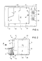
- FIGURE 2 shows a front view of the cover 2, on which bearing pins 12 and 13 are formed on opposite end faces, in such a way that the cover 2 represents a rocker in relation to the bearing axis.
- FIGURE 2 also shows that strips 14 and 15 are formed on the cover, which with Corresponding wall sections 16 and 17 formed on the upper part 4 of the housing 1 each form a fold connection which acts as a stop when the cover 2 is closed. With 18 a stop is designated, which takes effect when the cover 2 is pivoted into the open position.
- 19 represents a bolt which, as can be seen from FIG. 6, forms a locking mechanism with a spring-mounted armature 20 of an electromagnet 21, which causes the cover 2 to be locked when the electromagnet 21 is in the currentless state.
- FIG. 3 also shows threaded lugs 26 and 27 and bolts 28 and 29 which, as can be seen in FIGURE 4, reach through openings 30 and 31 in an intermediate base 32 formed on upper part 4 when the cover 2 is closed and hold the cover in the closed position .
- openings 33, 34, 35 and 36 and associated inward-facing receiving tubes for holding the photodiodes 8, 9, 10 and 11 and bearings 37 and 38 for guiding the buttons 6 and 7.
- a bore 42 provided in the intermediate floor 32 and provided with a counterbore serves to support a stylus 43 (FIGURE 6) which actuates a microswitch 44 which switches the read / write voltage supply for the data movement when both the cover 2 is closed, as well as a data memory 45 is used.
- FIGURE 5 shows that on the upper part 4 of the housing 1 spacers 46, 47, 48 and 49th are molded.
- a lower part 50 of the housing 1 carries the spacer pins 46, 47, 48 and 49 associated attachment posts, two of which are visible in FIGURE 5 and designated 51 and 52.
- the shoulder posts serve as a support for a printed circuit board 53, which carries corresponding edge recesses corresponding to the shoulder posts, two of which are shown in FIG. 5 and are designated by 54 and 55.
- the circuit board 53 carries the electronic components for the data transfer between the data storage 45 and sensors located outside the data storage device and / or a computer. It carries electrical components for the voltage supply, at least one adaptation interface and a program memory 56, which is shown in FIG. 5 as representative of the large number of electronic components.
- 57 designates one of two buttons 6 and 7 assigned to switches.
- 58, 59, 60 and 61 represent insulation sleeves assigned to the photodiode lines.
- the circuit board 53 is, as can be seen from FIG. 5, via a flexible conduction band 62 in electrical connection with a further circuit board 63, which is assigned to a plug base 64 and is mechanically and electrically connected to it via plug pins 65.
- This assembly is fastened to the cover 2 by means of screws, one of which - 66 - is shown, via the threaded attachments 26 and 27, in such a way that the plug base 64 is arranged in alignment with the guide profiles 22 and 23.
- the circuit board 53 and the cover 2 thus represent an assembly that can be checked before the data storage device is assembled.
- the circuit board 53 is inserted into the lower part 50 of the housing 1.
- the cover 2 is inserted through the opening 41 in the upper part 4 and snapped into the bearings 39 and 40.
- the lower part 50 and upper part 4 of the housing 1 are joined together and by means of through-bolts 67, 68, 69 and 49 which engage in the spacer bolts 46, 47, 48 and 49 70 screwed together, the circuit board 53 being held between the two housing parts 4 and 50.
- 71 shows a seal assigned to screw 67; 72 and 73 denote hook tapes which enable the data storage device to be fastened by means of a Velcro fastener.
- FIGURE 6 which shows the completed data storage device with inserted data storage 45
- the spring-loaded anchor 20 is accessible through an opening 74 in the upper part 4, which is assigned a seal 75, and can be operated by hand and thus, for example, in the event of a power failure the lid 2 can be unlocked.
- the flexible conduit band 62 which essentially corresponds to the width of the cover 2, can be designed to be resilient and can be preformed in such a way that the cover 2 pivots into the open position after unlocking by the conduction band 62, at least in this position, however is held.
Landscapes
- Engineering & Computer Science (AREA)
- Physics & Mathematics (AREA)
- General Physics & Mathematics (AREA)
- Theoretical Computer Science (AREA)
- Artificial Intelligence (AREA)
- Computer Vision & Pattern Recognition (AREA)
- Lock And Its Accessories (AREA)
- Time Recorders, Dirve Recorders, Access Control (AREA)
- Control Of Vending Devices And Auxiliary Devices For Vending Devices (AREA)
- Beverage Vending Machines With Cups, And Gas Or Electricity Vending Machines (AREA)
- Devices For Checking Fares Or Tickets At Control Points (AREA)
- Warehouses Or Storage Devices (AREA)
- Structure Of Receivers (AREA)
- Calculators And Similar Devices (AREA)
- Credit Cards Or The Like (AREA)
- Signal Processing For Digital Recording And Reproducing (AREA)
Applications Claiming Priority (2)
| Application Number | Priority Date | Filing Date | Title |
|---|---|---|---|
| DE3930545 | 1989-09-13 | ||
| DE3930545A DE3930545A1 (de) | 1989-09-13 | 1989-09-13 | Einrichtung zur aufnahme eines transportablen, karten- oder plattenfoermigen datenspeichers |
Publications (3)
| Publication Number | Publication Date |
|---|---|
| EP0417616A2 true EP0417616A2 (fr) | 1991-03-20 |
| EP0417616A3 EP0417616A3 (en) | 1991-06-05 |
| EP0417616B1 EP0417616B1 (fr) | 1994-11-17 |
Family
ID=6389320
Family Applications (1)
| Application Number | Title | Priority Date | Filing Date |
|---|---|---|---|
| EP90117030A Expired - Lifetime EP0417616B1 (fr) | 1989-09-13 | 1990-09-05 | Dispositif de réception d'une mémoire transportable de données présentée sous la forme d'une carte ou de forme plate |
Country Status (7)
| Country | Link |
|---|---|
| EP (1) | EP0417616B1 (fr) |
| JP (1) | JPH03105784A (fr) |
| AT (1) | ATE114198T1 (fr) |
| BR (1) | BR9004549A (fr) |
| DD (1) | DD297724A5 (fr) |
| DE (2) | DE3930545A1 (fr) |
| ES (1) | ES2065451T3 (fr) |
Cited By (2)
| Publication number | Priority date | Publication date | Assignee | Title |
|---|---|---|---|---|
| GB2250846B (en) * | 1990-12-13 | 1994-08-24 | Technophone Ltd | Card reader |
| FR2796763A1 (fr) * | 1999-07-23 | 2001-01-26 | Itt Mfg Enterprises Inc | Connecteur electrique pour carte a circuit(s) integre(s) comportant un commutateur de verrou du couvercle porte carte |
Families Citing this family (1)
| Publication number | Priority date | Publication date | Assignee | Title |
|---|---|---|---|---|
| DE102007024729A1 (de) * | 2007-05-25 | 2008-11-27 | Continental Automotive Gmbh | Elektrisches Gerät mit einer Datenträgerverriegelungseinrichtung und Verfahren zum Entriegeln eines Datenträgers |
Family Cites Families (5)
| Publication number | Priority date | Publication date | Assignee | Title |
|---|---|---|---|---|
| US4359222A (en) * | 1978-10-30 | 1982-11-16 | Smith Engineering | Hand-held electronic game playing device with replaceable cartridges |
| DE3303501A1 (de) * | 1983-02-02 | 1984-08-02 | Hegener + Glaser GmbH, 8000 München | Spielcomputer in modularbauweise |
| JPS6022795A (ja) * | 1983-07-18 | 1985-02-05 | Tokyo Tatsuno Co Ltd | 板状記憶媒体の読取り・書込み装置 |
| US4598962A (en) * | 1984-03-14 | 1986-07-08 | Motorola, Inc. | Memory device retaining apparatus for portable data processor |
| DE3736258A1 (de) * | 1987-10-27 | 1989-05-11 | Mannesmann Kienzle Gmbh | Datenkartenanordnung |
-
1989
- 1989-09-13 DE DE3930545A patent/DE3930545A1/de not_active Withdrawn
-
1990
- 1990-09-05 AT AT90117030T patent/ATE114198T1/de active
- 1990-09-05 EP EP90117030A patent/EP0417616B1/fr not_active Expired - Lifetime
- 1990-09-05 ES ES90117030T patent/ES2065451T3/es not_active Expired - Lifetime
- 1990-09-05 DE DE59007716T patent/DE59007716D1/de not_active Expired - Fee Related
- 1990-09-11 DD DD90343958A patent/DD297724A5/de not_active IP Right Cessation
- 1990-09-11 JP JP2239151A patent/JPH03105784A/ja active Pending
- 1990-09-12 BR BR909004549A patent/BR9004549A/pt not_active Application Discontinuation
Cited By (4)
| Publication number | Priority date | Publication date | Assignee | Title |
|---|---|---|---|---|
| GB2250846B (en) * | 1990-12-13 | 1994-08-24 | Technophone Ltd | Card reader |
| FR2796763A1 (fr) * | 1999-07-23 | 2001-01-26 | Itt Mfg Enterprises Inc | Connecteur electrique pour carte a circuit(s) integre(s) comportant un commutateur de verrou du couvercle porte carte |
| WO2001008266A1 (fr) * | 1999-07-23 | 2001-02-01 | Itt Manufacturing Enterprises Inc. | Connecteur electrique pour carte a puce, comprenant un commutateur de verrouillage du couvercle porte-carte |
| US6869302B2 (en) | 1999-07-23 | 2005-03-22 | Itt Manufacturing Enterprises, Inc. | Smart card connector with locking switch |
Also Published As
| Publication number | Publication date |
|---|---|
| JPH03105784A (ja) | 1991-05-02 |
| DD297724A5 (de) | 1992-01-16 |
| EP0417616B1 (fr) | 1994-11-17 |
| ATE114198T1 (de) | 1994-12-15 |
| ES2065451T3 (es) | 1995-02-16 |
| DE59007716D1 (de) | 1994-12-22 |
| EP0417616A3 (en) | 1991-06-05 |
| DE3930545A1 (de) | 1991-03-21 |
| BR9004549A (pt) | 1991-09-10 |
Similar Documents
| Publication | Publication Date | Title |
|---|---|---|
| EP0186737B1 (fr) | Dispositif d'introduction d'une carte de données à circuit électronique | |
| DE69834302T2 (de) | Chipkarten-Verbinder | |
| DE69230516T2 (de) | Tragfutteral für elektronische Speicherkarte | |
| DE69128365T2 (de) | Elektronisches System mit Erweiterungsvorrichtung zur Funktionenerweiterung eines kompakten elektronischen Gerätes | |
| DE4320683C2 (de) | Tragbares Informationsverarbeitungsgerät | |
| DE69227411T2 (de) | Elektronische Vorrichtung mit einer abnehmbaren Einheit ausgerüstet | |
| DE69030556T2 (de) | Tragbares Gerät mit abnehmarer Speichereinheit | |
| US5187646A (en) | Data storage device with an arrangement for receiving a transportable, card-shaped or disk-shaped data storage unit so that the data storage unit is inaccessible in an operating position | |
| DE29720521U1 (de) | Fahrtschreiber mit einem flachen, quaderförmigen Einbaugehäuse | |
| EP0417616B1 (fr) | Dispositif de réception d'une mémoire transportable de données présentée sous la forme d'une carte ou de forme plate | |
| EP0386664B1 (fr) | Réception de cartes de données | |
| WO1992022043A1 (fr) | Terminal intelligent utile comme support protege de donnees | |
| EP0534402A2 (fr) | Dispositif de déverrouillae d'un organe d'accrochage sous tension élastique, sur le côté d'un tiroir | |
| DE10112061B4 (de) | Aufnahmevorrichtung für in Fahrzeugen verwendete, der personenbezogenen Erfassung von Fahrtdaten dienende Chipkarten | |
| DE4120968C2 (fr) | ||
| DE19729218A1 (de) | Anordnung zum Erfassen und Auswerten von Zeit- und Betriebsdaten | |
| EP0902548B1 (fr) | Récepteur de radiodiffusion | |
| DE3422896C2 (fr) | ||
| EP0427172B1 (fr) | Micro-ordinateur avec unité de mémoire enfichable pour protection des données | |
| DE69304100T3 (de) | Abnehmbares Gerät für Autoradio | |
| DE1949412A1 (de) | Chassis fuer elektronische Geraete | |
| WO1993008571A1 (fr) | Lecteur de la memoire statique d'une cassette | |
| DE69509350T2 (de) | Schlossbedienungsmechanismus mit einem zweiteiligen Gehäuse | |
| DE29519209U1 (de) | Batteriefach zur Aufnahme von Batteriezellen | |
| DE3724284A1 (de) | Vorrichtung zur aufnahme von auswechselbaren baugruppen in einem elektronischen geraet |
Legal Events
| Date | Code | Title | Description |
|---|---|---|---|
| PUAI | Public reference made under article 153(3) epc to a published international application that has entered the european phase |
Free format text: ORIGINAL CODE: 0009012 |
|
| AK | Designated contracting states |
Kind code of ref document: A2 Designated state(s): AT CH DE ES FR GB IT LI NL SE |
|
| PUAL | Search report despatched |
Free format text: ORIGINAL CODE: 0009013 |
|
| RHK1 | Main classification (correction) |
Ipc: G07C 5/00 |
|
| AK | Designated contracting states |
Kind code of ref document: A3 Designated state(s): AT CH DE ES FR GB IT LI NL SE |
|
| 17P | Request for examination filed |
Effective date: 19911203 |
|
| RAP1 | Party data changed (applicant data changed or rights of an application transferred) |
Owner name: MANNESMANN KIENZLE GMBH |
|
| 17Q | First examination report despatched |
Effective date: 19940120 |
|
| GRAA | (expected) grant |
Free format text: ORIGINAL CODE: 0009210 |
|
| AK | Designated contracting states |
Kind code of ref document: B1 Designated state(s): AT CH DE ES FR GB IT LI NL SE |
|
| PG25 | Lapsed in a contracting state [announced via postgrant information from national office to epo] |
Ref country code: IT Free format text: LAPSE BECAUSE OF FAILURE TO SUBMIT A TRANSLATION OF THE DESCRIPTION OR TO PAY THE FEE WITHIN THE PRE;WARNING: LAPSES OF ITALIAN PATENTS WITH EFFECTIVE DATE BEFORE 2007 MAY HAVE OCCURRED AT ANY TIME BEFORE 2007. THE CORRECT EFFECTIVE DATE MAY BE DIFFERENT FROM THE ONE RECORDED.SCRIBED TIME-LIMIT Effective date: 19941117 Ref country code: NL Effective date: 19941117 |
|
| REF | Corresponds to: |
Ref document number: 114198 Country of ref document: AT Date of ref document: 19941215 Kind code of ref document: T |
|
| REF | Corresponds to: |
Ref document number: 59007716 Country of ref document: DE Date of ref document: 19941222 |
|
| GBT | Gb: translation of ep patent filed (gb section 77(6)(a)/1977) |
Effective date: 19950117 |
|
| REG | Reference to a national code |
Ref country code: ES Ref legal event code: FG2A Ref document number: 2065451 Country of ref document: ES Kind code of ref document: T3 |
|
| ET | Fr: translation filed | ||
| PG25 | Lapsed in a contracting state [announced via postgrant information from national office to epo] |
Ref country code: SE Effective date: 19950217 |
|
| NLV1 | Nl: lapsed or annulled due to failure to fulfill the requirements of art. 29p and 29m of the patents act | ||
| PGFP | Annual fee paid to national office [announced via postgrant information from national office to epo] |
Ref country code: AT Payment date: 19950823 Year of fee payment: 6 |
|
| PLBE | No opposition filed within time limit |
Free format text: ORIGINAL CODE: 0009261 |
|
| STAA | Information on the status of an ep patent application or granted ep patent |
Free format text: STATUS: NO OPPOSITION FILED WITHIN TIME LIMIT |
|
| 26N | No opposition filed | ||
| PGFP | Annual fee paid to national office [announced via postgrant information from national office to epo] |
Ref country code: CH Payment date: 19960314 Year of fee payment: 6 |
|
| PG25 | Lapsed in a contracting state [announced via postgrant information from national office to epo] |
Ref country code: AT Effective date: 19960905 |
|
| PG25 | Lapsed in a contracting state [announced via postgrant information from national office to epo] |
Ref country code: CH Effective date: 19960930 Ref country code: LI Effective date: 19960930 |
|
| REG | Reference to a national code |
Ref country code: CH Ref legal event code: PL |
|
| PGFP | Annual fee paid to national office [announced via postgrant information from national office to epo] |
Ref country code: ES Payment date: 19970926 Year of fee payment: 8 |
|
| PG25 | Lapsed in a contracting state [announced via postgrant information from national office to epo] |
Ref country code: ES Free format text: LAPSE BECAUSE OF EXPIRATION OF PROTECTION Effective date: 19980907 |
|
| PGFP | Annual fee paid to national office [announced via postgrant information from national office to epo] |
Ref country code: GB Payment date: 19990813 Year of fee payment: 10 |
|
| PG25 | Lapsed in a contracting state [announced via postgrant information from national office to epo] |
Ref country code: GB Free format text: LAPSE BECAUSE OF NON-PAYMENT OF DUE FEES Effective date: 20000905 |
|
| REG | Reference to a national code |
Ref country code: ES Ref legal event code: FD2A Effective date: 20010201 |
|
| GBPC | Gb: european patent ceased through non-payment of renewal fee |
Effective date: 20000905 |
|
| PGFP | Annual fee paid to national office [announced via postgrant information from national office to epo] |
Ref country code: DE Payment date: 20010903 Year of fee payment: 12 |
|
| PGFP | Annual fee paid to national office [announced via postgrant information from national office to epo] |
Ref country code: FR Payment date: 20020930 Year of fee payment: 13 |
|
| PG25 | Lapsed in a contracting state [announced via postgrant information from national office to epo] |
Ref country code: DE Free format text: LAPSE BECAUSE OF NON-PAYMENT OF DUE FEES Effective date: 20030401 |
|
| PG25 | Lapsed in a contracting state [announced via postgrant information from national office to epo] |
Ref country code: FR Free format text: LAPSE BECAUSE OF NON-PAYMENT OF DUE FEES Effective date: 20040528 |
|
| REG | Reference to a national code |
Ref country code: FR Ref legal event code: ST |