EP0417748A2 - Unterbrechungssteuerungsschaltung für Verwendung in einem Einchip-Mikrorechner - Google Patents
Unterbrechungssteuerungsschaltung für Verwendung in einem Einchip-Mikrorechner Download PDFInfo
- Publication number
- EP0417748A2 EP0417748A2 EP90117524A EP90117524A EP0417748A2 EP 0417748 A2 EP0417748 A2 EP 0417748A2 EP 90117524 A EP90117524 A EP 90117524A EP 90117524 A EP90117524 A EP 90117524A EP 0417748 A2 EP0417748 A2 EP 0417748A2
- Authority
- EP
- European Patent Office
- Prior art keywords
- interrupt
- interrupt request
- control circuit
- chip microcomputer
- data
- Prior art date
- Legal status (The legal status is an assumption and is not a legal conclusion. Google has not performed a legal analysis and makes no representation as to the accuracy of the status listed.)
- Withdrawn
Links
Images

Classifications
-
- G—PHYSICS
- G06—COMPUTING OR CALCULATING; COUNTING
- G06F—ELECTRIC DIGITAL DATA PROCESSING
- G06F11/00—Error detection; Error correction; Monitoring
- G06F11/22—Detection or location of defective computer hardware by testing during standby operation or during idle time, e.g. start-up testing
- G06F11/2205—Detection or location of defective computer hardware by testing during standby operation or during idle time, e.g. start-up testing using arrangements specific to the hardware being tested
- G06F11/2231—Detection or location of defective computer hardware by testing during standby operation or during idle time, e.g. start-up testing using arrangements specific to the hardware being tested to test interrupt circuits
-
- G—PHYSICS
- G06—COMPUTING OR CALCULATING; COUNTING
- G06F—ELECTRIC DIGITAL DATA PROCESSING
- G06F13/00—Interconnection of, or transfer of information or other signals between, memories, input/output devices or central processing units
- G06F13/14—Handling requests for interconnection or transfer
- G06F13/20—Handling requests for interconnection or transfer for access to input/output bus
- G06F13/24—Handling requests for interconnection or transfer for access to input/output bus using interrupt
-
- G—PHYSICS
- G06—COMPUTING OR CALCULATING; COUNTING
- G06F—ELECTRIC DIGITAL DATA PROCESSING
- G06F13/00—Interconnection of, or transfer of information or other signals between, memories, input/output devices or central processing units
- G06F13/14—Handling requests for interconnection or transfer
- G06F13/20—Handling requests for interconnection or transfer for access to input/output bus
- G06F13/24—Handling requests for interconnection or transfer for access to input/output bus using interrupt
- G06F13/26—Handling requests for interconnection or transfer for access to input/output bus using interrupt with priority control
-
- G—PHYSICS
- G06—COMPUTING OR CALCULATING; COUNTING
- G06F—ELECTRIC DIGITAL DATA PROCESSING
- G06F9/00—Arrangements for program control, e.g. control units
- G06F9/06—Arrangements for program control, e.g. control units using stored programs, i.e. using an internal store of processing equipment to receive or retain programs
- G06F9/46—Multiprogramming arrangements
Definitions
- This invention relates to an interrupt control circuit for use in a 1-chip microcomputer, and more particularly to an interrupt control circuit having priority determining means which is easy to inspect.
- An interrupt control circuit for use in a microcomputer or the like determines priority of a plurality of interrupt requests, and outputs to the CPU a request of the highest priority.
- the conventional interrupt control circuit has a plurality of interrupt request latches. Each of the latches is set in response to interrupt request signal sent from interrupt request means such as a serial or parallel input/output circuit, an A/D converter, a timer, or the like, and reset in response to an interrupt request clear signal.
- interrupt request means such as a serial or parallel input/output circuit, an A/D converter, a timer, or the like.
- the interrupt control circuit is an LSI circuit such as 1-chip microcomputer
- an interrupt request signal can be input through a terminal of the microcomputer.
- a desired inspection pattern is supplied from an external circuit, thereby setting each interrupt request latch to a desired state.
- interrupt control circuit In contrast, if the interrupt control circuit is incorporated in a 1-chip microcomputer, an interrupt request signal is directly input to the circuit from the input/output circuit also incorporated in the microcomputer, not from an external circuit. In this case, in order to set a specific interrupt request latch to a desired state, the input/output circuit connected to the interrupt request latch must be set to an appropriate state. This is a critical drawback in inspecting the priority determining means used in the interrupt control circuit in three respects. First, the interrupt control circuit cannot be inspected independently. Second, a great number of inspection patterns must be input to inspect many combinations of circuits, which may lengthen the inspecting time very much. Third, the inspection patterns required may be very complicated.
- the second and third drawbacks are prominent, especially when the input/output circuit has many functions, and a great number of interrupt request signals are therefore generated.
- the second and third drawbacks are also great, when the input/output circuit includes a timer, which outputs signals at regular intervals.
- the conventional interrupt control circuit for use in a 1-chip microcomputer is disadvantageous in that a long period of time is required for inspecting the priority determining function, and the inspecting operation is complicated.
- the present invention has been made in consideration of the above circumstances, and its object is to provide an interrupt control circuit for use in a 1-chip microcomputer having priority determining means which is easy to inspect.
- an interrupt control circuit for use in a 1-chip microcomputer, comprising a CPU, a plurality of interrupt request means, each generating interrupt request signals to be supplied to the CPU, and interrupt control/priority determining means, connected to the CPU via an internal data bus, supplied with the interrupt request signals generated by the plurality of interrupt request means for determining the priority of the interrupt request signals and outputting the highest priority interrupt request signals to the CPU, and supplied with an interrupt request signal from the CPU through the internal data bus.
- an interrupt control circuit for use in a 1-chip microcomputer, comprising a CPU, a plurality of interrupt request means, each generating interrupt request signals to be supplied to the CPU, mode data storing means for storing mode data for discriminating between a normal operation mode and an inspection mode, a plurality of interrupt request latching means for latching the interrupt request signals from the interrupt request means when the mode data storing means stores data corresponding to the normal operation mode, and latching data on the internal data bus as an interrupt request signal when the mode data storing means stores data corresponding to the inspection mode, and a priority determining means for determining the priority of the interrupt requests stored in the plurality of interrupt request holding means.
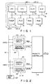
- Fig. 1 shows the entire structure of a 1-chip microcomputer including an interrupt control circuit according to the present invention.
- the 1-chip microcomputer comprises central processing unit (CPU) 11, interrupt control circuit (IRC) 12, serial input/output circuit (SI/O) 13, analog/digital converter (A/D) 14, timer 15, parallel input/output circuit (PI/O) 16, random access memory (RAM) 17, and read-only memory (ROM) 18, all of which are connected to one another through internal data bus 19.
- CPU central processing unit
- IRC interrupt control circuit
- SI/O serial input/output circuit
- A/D analog/digital converter
- PI/O parallel input/output circuit
- RAM random access memory
- ROM read-only memory
- interrupt request means which request interrupt for CPU 11.
- These interrupt request means output interrupt request signals, which are supplied to interrupt control circuit 12 through exclusive interrupt signal lines 20-1 to 20-4.
- interrupt control circuit 12 receives interrupt request signals, it determines the priority of the interrupt request signals in accordance with the predetermined priority of the interrupt requesting means and the priority level of the request signals output from each interrupt request means, and supplies the highest priority interrupt request signal to CPU 11.
- FIG. 2 shows interrupt control circuit (IRC) 12 shown in Fig. 1.
- Interrupt control circuit (IRC) 12 comprises four interrupt processing circuits 21-1 to 21-4 corresponding to the above-mentioned four interrupt request means, serial input/output circuit 13, analog/digital converter 14, timer 15, and parallel input/output circuit 18.
- Interrupt control circuit (IRC) 12 also comprises mode register 22 and priority controller 23 both of which are common to those interrupt processing circuits 21-1 to 21-4.
- Each of interrupt processing circuits 21-1 to 21-4 has control circuit 24 and control register 25.
- each interrupt processing circuit the interrupt request signal IREQ from an interrupt request means or the data supplied through internal data bus 19 is latched by an internal latch and subjected to a predetermined processing. Then, the processed data is output as an interrupt signal REQ to priority controller 23.
- Control register 25 stores data representing the interrupt priority levels of interrupt request signals from the interrupt request means, which is output as a level signal LEVEL to priority controller 23 together with the above-mentioned interrupt signal REQ.
- Priority controller 23 determines the priority of the interrupt request signals in accordance with the signals output from interrupt processing circuits 21-1 to 21-4, and transmits the highest priority interrupt request signal to CPU 11.
- Fig. 3 is a circuit diagram showing in detail the structure of the interrupt processing circuits 21-1 to 21-4. Since all of circuits 21-1 to 21-4 have the same structure, only circuit 21-1 will be described below.
- Internal data bus 19 transmits data constituted by a plurality of bits, and data of the least significant bit DB0 is supplied to the data input terminal (D) of 1-bit latch circuit 31.
- a write control signal WSTB is supplied to the control input terminal (G) of latch control circuit 31.
- An output signal of AND gate circuit 32 is supplied to the clear input terminal (C) of latch control circuit 31.
- Date MODE stored in mode register 22 is supplied to one of the two input terminals of AND gate circuit 32 via inverter 33, and a system reset signal RESET is supplied to the other input terminal thereof.
- the interrupt request signal IREQ output from the interrupt request means is supplied to the control terminal (G) of 1-bit latch circuit 34.
- the data input terminal (D) of latch circuit 34 is connected to the power source set at a "H" level.
- the output signal of three-inputs AND gate circuit 35 is supplied to the clear input terminal (C) of latch circuit 34.
- the above-mentioned data MODE is input to a first input terminal of AND gate circuit 35, the system reset signal RESET to a second input terminal, and the output signal of NAND gate circuit 36 to a third input terminal.
- Data of the least significant bit DB0 of internal data but 19 is supplied to one of the input terminals of NAND gate circuit 36 via inverter 37, and the write control signal WSTB is supplied to the other input terminals thereof.
- Signals output from the output terminals (Q) of latch circuits 31 and 34 are supplied in parallel to the input terminals of two-inputs OR gate circuit 38.
- An output signal of OR gate circuit 38 is supplied to the data input terminal (D) of timing set 1-bit latch circuit 39, and also to the least significant bit DB0 of internal data but 19 through transfer gate 40.
- a timing signal TMG is supplied from a timing signal generating circuit (not shown) to the control input terminal (G) of latch circuit 39.
- An output signal from the terminal (Q) of latch circuit 39 is supplied to one of the input terminals of AND gate circuit 41.
- 1-bit latch circuit 42 serves as a mask for masking an interrupt request signal.
- Data of the bit DB1, the bit immediately upper than the least significant bit DBO of internal data bus 19, is supplied to the data input terminal (D) of latch circuit 42.
- the mask signal MASK is supplied to the control input terminal (G) of latch circuit 42.
- An output signal from the output terminal ( Q ) of latch circuit 42 is supplied to the other input terminal of AND gate circuit 41.
- An output signal from the output terminal (Q) of latch circuit 42 is supplied to DB1 of internal data bus 19 via transfer gate 43.
- Transfer gates 40 and 43 are operated under control of a read control signal RSTB.
- the other interrupt processing circuits 21-2 to 21-4 have the same structure as the above-described circuit 21-1, except for the bit of the internal data bus.
- Fig. 4 shows the memory state of each of control registers 25 shown in Fig. 2.
- data of three interrupt priority levels is written in the control register.
- the signals RSTB and WSTB are respectively used to read/write data from/into control register 25. These signals are set by software executed by CPU 11 (Fig. 1).
- the data representing one of the three interrupt priority levels is supplied to priority controller 23, and utilized therein to determine the priority of the interrupt request signals.
- CPU 11 causes mode register 22 to store data through software processing. For example, "1" level data is stored in mode register 22 in a normal operation, and "0" level data in an inspection mode.
- a system reset signal RESET is set to a “0" level.
- the output signals of AND gate circuits 32 and 35 are also set to a “0” level, with the result that latch circuits 31 and 34 are reset. Thereafter, system reset signal RESET rises to a "1" level.
- mode data MODE of "0" level is stored in mode register 22 by software processing of CPU 11.
- the output of AND gate circuit 35 is set to "0" level and latch circuit 34 is set to the cleared state, while the output of AND gate circuit 32 is set to "1" level and latch circuit 31 is released from the reset state.
- Latch circuit 31 latches data of DB0 of internal data bus 19, and the output signal from the terminal (Q) is supplied through OR gate circuit 38 to latch circuit 39.
- a timing signal TMG is supplied from a timing signal generating circuit (not shown) to latch circuit 39, the output at the terminal (Q) of latch circuit 39 is set in response to the signal supplied to the data input terminal.
- AND gate circuit 41 outputs an interrupt request signal REQ to priority controller 23, in accordance with the level at the output terminal ( Q ) of latch circuit 42 in a masking state or a non-masking state.
- latch circuit 42 To set latch circuit 42 to a masking state, "1" level data is supplied to DB1 of internal data bus 19. and a signal WSTB is supplied to latch circuit 42, thereby setting the output terminal ( Q ) of latch circuit 42 to a "0" level.
- Output signals from terminals (Q) of latch circuits 31 and 34 can be output to DB0 of internal data bus 19, and an output signal from the output terminal (Q) of latch circuit 42 can be output to DB1.
- the data reading is performed in response to a read control signal RSTB.
- the present invention provides an interrupt control circuit for use in a 1-chip microcomputer having priority determining means which is easy to inspect.
Landscapes
- Engineering & Computer Science (AREA)
- Theoretical Computer Science (AREA)
- General Engineering & Computer Science (AREA)
- Physics & Mathematics (AREA)
- General Physics & Mathematics (AREA)
- Software Systems (AREA)
- Computer Hardware Design (AREA)
- Quality & Reliability (AREA)
- Microcomputers (AREA)
- Bus Control (AREA)
- Test And Diagnosis Of Digital Computers (AREA)
Applications Claiming Priority (2)
| Application Number | Priority Date | Filing Date | Title |
|---|---|---|---|
| JP1234956A JPH0397036A (ja) | 1989-09-11 | 1989-09-11 | 割込み制御回路 |
| JP234956/89 | 1989-09-11 |
Publications (2)
| Publication Number | Publication Date |
|---|---|
| EP0417748A2 true EP0417748A2 (de) | 1991-03-20 |
| EP0417748A3 EP0417748A3 (en) | 1992-01-08 |
Family
ID=16978894
Family Applications (1)
| Application Number | Title | Priority Date | Filing Date |
|---|---|---|---|
| EP19900117524 Withdrawn EP0417748A3 (en) | 1989-09-11 | 1990-09-11 | Interrupt control circuit for use in 1-chip microcomputer |
Country Status (3)
| Country | Link |
|---|---|
| EP (1) | EP0417748A3 (de) |
| JP (1) | JPH0397036A (de) |
| KR (1) | KR930005771B1 (de) |
Cited By (4)
| Publication number | Priority date | Publication date | Assignee | Title |
|---|---|---|---|---|
| EP0619899A4 (de) * | 1992-01-02 | 1994-09-02 | Amdahl Corp | Anwendungs-software für hardware-unterbrechungen. |
| WO1997044734A1 (en) * | 1996-05-17 | 1997-11-27 | Advanced Micro Devices, Inc. | System and method for testing and debugging a multiprocessing interrupt controller |
| CN111552599A (zh) * | 2020-04-26 | 2020-08-18 | 武汉精测电子集团股份有限公司 | 一种分布式进程处理系统、半导体老化测试方法及系统、分布式系统 |
| CN114860630A (zh) * | 2022-04-27 | 2022-08-05 | 深圳市洛仑兹技术有限公司 | 一种数字处理电路、信号处理方法 |
Families Citing this family (2)
| Publication number | Priority date | Publication date | Assignee | Title |
|---|---|---|---|---|
| KR100393765B1 (ko) * | 1996-03-26 | 2004-03-10 | 엘지전자 주식회사 | 인터럽트제어장치 |
| KR100575608B1 (ko) * | 1998-10-09 | 2006-09-28 | 매그나칩 반도체 유한회사 | 버스 제어회로 |
Family Cites Families (2)
| Publication number | Priority date | Publication date | Assignee | Title |
|---|---|---|---|---|
| JPS5232236A (en) * | 1975-09-05 | 1977-03-11 | Toshiba Corp | Testing device for interrupt processing circuit |
| JPS52156528A (en) * | 1976-06-22 | 1977-12-27 | Mitsubishi Electric Corp | Micro-processor interruption controller |
-
1989
- 1989-09-11 JP JP1234956A patent/JPH0397036A/ja active Pending
-
1990
- 1990-09-11 EP EP19900117524 patent/EP0417748A3/en not_active Withdrawn
- 1990-09-11 KR KR1019900014301A patent/KR930005771B1/ko not_active Expired - Fee Related
Cited By (6)
| Publication number | Priority date | Publication date | Assignee | Title |
|---|---|---|---|---|
| EP0619899A4 (de) * | 1992-01-02 | 1994-09-02 | Amdahl Corp | Anwendungs-software für hardware-unterbrechungen. |
| WO1997044734A1 (en) * | 1996-05-17 | 1997-11-27 | Advanced Micro Devices, Inc. | System and method for testing and debugging a multiprocessing interrupt controller |
| CN111552599A (zh) * | 2020-04-26 | 2020-08-18 | 武汉精测电子集团股份有限公司 | 一种分布式进程处理系统、半导体老化测试方法及系统、分布式系统 |
| CN111552599B (zh) * | 2020-04-26 | 2024-04-09 | 武汉精测电子集团股份有限公司 | 一种分布式进程处理系统、半导体老化测试方法及系统、分布式系统 |
| CN114860630A (zh) * | 2022-04-27 | 2022-08-05 | 深圳市洛仑兹技术有限公司 | 一种数字处理电路、信号处理方法 |
| CN114860630B (zh) * | 2022-04-27 | 2023-04-18 | 深圳市洛仑兹技术有限公司 | 一种数字处理电路、信号处理方法 |
Also Published As
| Publication number | Publication date |
|---|---|
| KR910006855A (ko) | 1991-04-30 |
| JPH0397036A (ja) | 1991-04-23 |
| EP0417748A3 (en) | 1992-01-08 |
| KR930005771B1 (ko) | 1993-06-24 |
Similar Documents
| Publication | Publication Date | Title |
|---|---|---|
| US4271466A (en) | Direct memory access control system with byte/word control of data bus | |
| US4716526A (en) | Multiprocessor system | |
| US4467420A (en) | One-chip microcomputer | |
| US5083260A (en) | Bus arbitration system for concurrent use of a system bus by more than one device | |
| WO1999056217A1 (en) | Interrupt controller | |
| EP0529677A1 (de) | Vielfachkanalschnittstelle in einem Mikrocomputer | |
| EP0408353B1 (de) | Integrierte Halbleiterschaltung | |
| US4628448A (en) | Operation mode setting apparatus on a single chip microprocessor | |
| EP0377455B1 (de) | Prüfmodusumschaltsystem für LSI | |
| US5159263A (en) | Lsi system having a test facilitating circuit | |
| US6874049B1 (en) | Semaphores with interrupt mechanism | |
| EP0184639B1 (de) | Testsystem für eine Tastaturschnittstellenschaltung | |
| KR930005771B1 (ko) | 인터럽트 제어회로 | |
| JPS6242306B2 (de) | ||
| US5341380A (en) | Large-scale integrated circuit device | |
| JPS6316316A (ja) | リセツト装置 | |
| JP2571090B2 (ja) | アドレス送信装置及び受信装置 | |
| JPS6491235A (en) | Control system for counter circuit | |
| JP2575895B2 (ja) | 集積回路の制御信号切換装置 | |
| JPH09305485A (ja) | 画像メモリ制御方式 | |
| JP2814849B2 (ja) | 通信制御装置 | |
| JPS622344A (ja) | 情報伝達装置 | |
| KR920009452B1 (ko) | 32비트 마이크로 프로세서를 이용한 64비트 데이타전송회로 | |
| JPS60117847A (ja) | デ−タ制御回路 | |
| JPH05241900A (ja) | コンピュータのプログラム動作確認方式 |
Legal Events
| Date | Code | Title | Description |
|---|---|---|---|
| PUAI | Public reference made under article 153(3) epc to a published international application that has entered the european phase |
Free format text: ORIGINAL CODE: 0009012 |
|
| 17P | Request for examination filed |
Effective date: 19900911 |
|
| AK | Designated contracting states |
Kind code of ref document: A2 Designated state(s): DE FR GB |
|
| PUAL | Search report despatched |
Free format text: ORIGINAL CODE: 0009013 |
|
| AK | Designated contracting states |
Kind code of ref document: A3 Designated state(s): DE FR GB |
|
| 17Q | First examination report despatched |
Effective date: 19940803 |
|
| STAA | Information on the status of an ep patent application or granted ep patent |
Free format text: STATUS: THE APPLICATION IS DEEMED TO BE WITHDRAWN |
|
| 18D | Application deemed to be withdrawn |
Effective date: 19941214 |