EP0418423B2 - Procédé d'attaque anisotrope de silicium - Google Patents
Procédé d'attaque anisotrope de silicium Download PDFInfo
- Publication number
- EP0418423B2 EP0418423B2 EP89117581A EP89117581A EP0418423B2 EP 0418423 B2 EP0418423 B2 EP 0418423B2 EP 89117581 A EP89117581 A EP 89117581A EP 89117581 A EP89117581 A EP 89117581A EP 0418423 B2 EP0418423 B2 EP 0418423B2
- Authority
- EP
- European Patent Office
- Prior art keywords
- groove
- etching
- silicon wafer
- structures
- mask
- Prior art date
- Legal status (The legal status is an assumption and is not a legal conclusion. Google has not performed a legal analysis and makes no representation as to the accuracy of the status listed.)
- Expired - Lifetime
Links
Images


Classifications
-
- G—PHYSICS
- G02—OPTICS
- G02B—OPTICAL ELEMENTS, SYSTEMS OR APPARATUS
- G02B6/00—Light guides; Structural details of arrangements comprising light guides and other optical elements, e.g. couplings
- G02B6/24—Coupling light guides
- G02B6/36—Mechanical coupling means
- G02B6/3628—Mechanical coupling means for mounting fibres to supporting carriers
- G02B6/3684—Mechanical coupling means for mounting fibres to supporting carriers characterised by the manufacturing process of surface profiling of the supporting carrier
- G02B6/3692—Mechanical coupling means for mounting fibres to supporting carriers characterised by the manufacturing process of surface profiling of the supporting carrier with surface micromachining involving etching, e.g. wet or dry etching steps
-
- H—ELECTRICITY
- H10—SEMICONDUCTOR DEVICES; ELECTRIC SOLID-STATE DEVICES NOT OTHERWISE PROVIDED FOR
- H10P—GENERIC PROCESSES OR APPARATUS FOR THE MANUFACTURE OR TREATMENT OF DEVICES COVERED BY CLASS H10
- H10P50/00—Etching of wafers, substrates or parts of devices
- H10P50/60—Wet etching
- H10P50/64—Wet etching of semiconductor materials
- H10P50/642—Chemical etching
- H10P50/644—Anisotropic liquid etching
-
- H—ELECTRICITY
- H10—SEMICONDUCTOR DEVICES; ELECTRIC SOLID-STATE DEVICES NOT OTHERWISE PROVIDED FOR
- H10P—GENERIC PROCESSES OR APPARATUS FOR THE MANUFACTURE OR TREATMENT OF DEVICES COVERED BY CLASS H10
- H10P50/00—Etching of wafers, substrates or parts of devices
- H10P50/69—Etching of wafers, substrates or parts of devices using masks for semiconductor materials
- H10P50/691—Etching of wafers, substrates or parts of devices using masks for semiconductor materials for Group V materials or Group III-V materials
-
- G—PHYSICS
- G02—OPTICS
- G02B—OPTICAL ELEMENTS, SYSTEMS OR APPARATUS
- G02B6/00—Light guides; Structural details of arrangements comprising light guides and other optical elements, e.g. couplings
- G02B6/24—Coupling light guides
- G02B6/36—Mechanical coupling means
- G02B6/3628—Mechanical coupling means for mounting fibres to supporting carriers
- G02B6/3648—Supporting carriers of a microbench type, i.e. with micromachined additional mechanical structures
- G02B6/3652—Supporting carriers of a microbench type, i.e. with micromachined additional mechanical structures the additional structures being prepositioning mounting areas, allowing only movement in one dimension, e.g. grooves, trenches or vias in the microbench surface, i.e. self aligning supporting carriers
Definitions
- the invention relates to a method for anisotropic Etching silicon according to the preamble of the claim 1.
- Single crystalline silicon is used because of its good micromechanical Properties more often than Starting material for various mechanical Components used.
- the possible uses range from pressure sensors to nozzles, for example for inkjet printers up to electro-optical Converter modules in hybrid construction technology.
- the structuring method represents the anisotropic etching of single-crystal silicon, for example in potassium hydroxide solution or ethylenediamine. However, this often disturbs severe undercutting of convex or protruding Corners. Such convex corners are for one for certain Applications necessary shaping, at the merging structures of different Size can be etched out of a silicon wafer must, inevitable.
- Such a structure will for example with optical transmit and receive modules for inserting a glass fiber and a ball lens needed.
- Such a transmission and reception module is in DE-OS 38 09 396 described in more detail.
- This optoelectronic converter module are the individual optical, optoelectronic and electro-optical Components directly on a silicon substrate arranged. For inserting the glass fiber and the ball lens the Si wafer is structured so that a narrow one V-groove for the glass fiber in a wide V-groove for receiving the ball lens opens.
- the invention is based on the object Avoid disadvantages and a multi-step process to create in the anisotropic etching of silicon with which it is possible to undercut convex or prevent protruding corners.
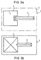
- the multi-step etching method according to the invention is the example of the confluence shown in FIG 1 a narrow V-groove 2 in a wide V-groove 3, the are anisotropically etched out of a Si wafer 1, in detail described.
- Such a structure is used in optical Transmitter and receiver modules for inserting one Glass fiber and a spherical lens are required as at the beginning already in connection with DE-OS 38 09 396 has been explained.
- FIG 2a and 2b In the usual manufacturing process shown in FIG 2a and 2b is based on a (100) -oriented Si wafer 1 parallel to the crystallographic (110) direction an Si oxide or nitride mask 4 is applied and then in potash lye or a mixture of pyrocatechol, Etched ethylenediamine and water. All known anisotropic etching mixtures is common, that the (111) planes are considerably slower than all the others Levels are attacked. This creates V-shaped etching pits 2 and 3, which concave from each other (111) planes are limited. At the two convex corners KE (FIG 2a) occur strong undercuts U on (FIG 2b), making it impossible later is to insert a ball lens into the large V-groove 3.
- KE convex corners
- an already structured silicon wafer 1 is present before the second etching step, which then already contains the V-groove 2, for example.
- this wafer 1 is coated accordingly.
- the paint adhesion is not completely perfect. According to a development of the invention, provision is therefore made to bury a mask for the second etching step before the first anisotropic etching, in order to then expose it again after the first etching.
- the thin oxide layer on the silicon nitride can therefore be etched off without significantly attacking the SiO 2 mask on the silicon.
- the silicon nitride can then be etched out, so that only the SiO 2 mask remains as a further masking layer 4 for etching out the following individual structure, for example the large V-groove.
- the individual process steps are shown using the example of the material combination Si 3 N 4 -SiO 2 in FIGS. 4a to 4f.
- FIG. 4a shows the coating with a photoresist layer F and the exposure in the direction of arrow B of the Si 3 N 4 layer located on the Si wafer 1, for example for etching a large V-groove.
- 4b shows the structuring of the Si 3 N 4 layer.
- 4c shows the oxidation with formation of the SiO 2 layer, the coating in the form of the photoresist layer F and the exposure indicated by arrows B, for example for a small V-groove.
- FIG. 4d describes the SiO 2 etching and the etching of the small V-groove 2.
- FIG 4e shows the oxidation of the small V-groove 2 with formation of the SiO 2 layer or the formation of the further masking layer 4 for the etching of the large V -Nut 3
- FIG 4f shows as a last step the etching away of the Si 3 N 4 layer and the etching out of the large V-groove 3 from the Si wafer 1.
Landscapes
- Physics & Mathematics (AREA)
- General Physics & Mathematics (AREA)
- Optics & Photonics (AREA)
- Weting (AREA)
Claims (4)
- Procédé d'attaque anisotrope de silicium, dans lequel on forme par attaque de la surface d'une galette de silicium à orientation (100), en utilisant un masque approprié et un réactif approprié d'attaque, des structures sans interruption de l'une à l'autre de dimensions différentes et de profondeurs différentes, les structures ayant la forme d'une petite rainure en V et d'un renfoncement plus grand en forme de V et dans lequel on forme par attaque de la galette de silicium, en au moins deux étapes d'attaque successives, les structures par masquage adéquat décomposées en structures distinctes se chevauchant, caractérisé en ce que l'on revêt, entre les étapes d'attaque, les structures (2) déjà attaquées, d'une autre couche (4) de masquage pour former par attaque les structures (3) suivantes,l'on forme par attaque d'une galette (1) de silicium et munie d'un masque adéquat, comme structure dans une première étape d'attaque, la petite rainure (2) en V,puis on recouvre la galette (1) de silicium et la petite rainure (2) en V d'un autre masque (4) destiné au renfoncement (3) plus grand en forme de V et ayant un retroussement dans lequel débouche l'ouverture (5) de masque ménagée pour le renfoncement plus grand en forme de V à la petite rainure (2) en forme de V, etensuite, on forme par attaque dans une seconde étape d'attaque, comme structure, le renfoncement (3) plus grand en forme de V, dans lequel débouche la petite rainure (2) en V, avec attaque latérale du retroussement.
- Procédé suivant la revendication 1, caractérisé en ce que l'on dépose l'autre masque (4) comme négatif sous forme d'un masque enterré, avant l'attaque anisotrope, sur la galette (1) de silicium.
- Procédé suivant la revendication 2, caractérisé en ce que l'on dépose comme négatif d'un masque enterré, une couche de nitrure de silicium sur la galette (1) de silicium.
- Procédé suivant la revendication 2 ou 3, caractérisé en ce que l'on produit l'autre masque (4) par oxydation thermique des parties, structurées au préalable, de la galette (1) de silicium.
Priority Applications (3)
| Application Number | Priority Date | Filing Date | Title |
|---|---|---|---|
| DE58909602T DE58909602D1 (de) | 1989-09-22 | 1989-09-22 | Verfahren zum anisotropen Ätzen von Silizium |
| EP89117581A EP0418423B2 (fr) | 1989-09-22 | 1989-09-22 | Procédé d'attaque anisotrope de silicium |
| JP2248604A JPH03132031A (ja) | 1989-09-22 | 1990-09-17 | シリコンの異方性エツチング方法 |
Applications Claiming Priority (1)
| Application Number | Priority Date | Filing Date | Title |
|---|---|---|---|
| EP89117581A EP0418423B2 (fr) | 1989-09-22 | 1989-09-22 | Procédé d'attaque anisotrope de silicium |
Publications (3)
| Publication Number | Publication Date |
|---|---|
| EP0418423A1 EP0418423A1 (fr) | 1991-03-27 |
| EP0418423B1 EP0418423B1 (fr) | 1996-02-07 |
| EP0418423B2 true EP0418423B2 (fr) | 1998-12-09 |
Family
ID=8201919
Family Applications (1)
| Application Number | Title | Priority Date | Filing Date |
|---|---|---|---|
| EP89117581A Expired - Lifetime EP0418423B2 (fr) | 1989-09-22 | 1989-09-22 | Procédé d'attaque anisotrope de silicium |
Country Status (3)
| Country | Link |
|---|---|
| EP (1) | EP0418423B2 (fr) |
| JP (1) | JPH03132031A (fr) |
| DE (1) | DE58909602D1 (fr) |
Families Citing this family (14)
| Publication number | Priority date | Publication date | Assignee | Title |
|---|---|---|---|---|
| DE4129206C2 (de) * | 1991-09-03 | 1995-01-05 | Bosch Gmbh Robert | Verfahren zur Strukturierung von Wafern |
| GB9203128D0 (en) * | 1992-02-14 | 1992-04-01 | Lucas Ind Plc | Alignment device for optical fibre |
| JP3205103B2 (ja) * | 1993-01-07 | 2001-09-04 | 松下電器産業株式会社 | 半導体装置の製造方法 |
| US5338400A (en) * | 1993-02-25 | 1994-08-16 | Ic Sensors, Inc. | Micromachining process for making perfect exterior corner in an etchable substrate |
| US5550088A (en) * | 1993-06-02 | 1996-08-27 | Lucent Technologies Inc. | Fabrication process for a self-aligned optical subassembly |
| JP3345518B2 (ja) * | 1994-09-28 | 2002-11-18 | 株式会社東芝 | 光半導体モジュールの製造方法 |
| US5935451A (en) * | 1997-02-24 | 1999-08-10 | Lucent Technologies Inc. | Fabrication of etched features |
| FR2761199B1 (fr) * | 1997-03-21 | 1999-04-16 | Commissariat Energie Atomique | Procede de realisation de deux cavites communicantes dans un substrat en materiau monocristallin par gravure chimique anisotrope |
| DE19725720A1 (de) * | 1997-06-18 | 1998-12-24 | Alsthom Cge Alcatel | Optischer Isolator und Wellenlängenmuliplexer-Modul mit integriertem optischen Isolator |
| DE10104324A1 (de) * | 2001-01-24 | 2002-08-01 | Siemens Ag | Verfahren zum Ätz-Strukturieren der Oberfläche eines Bauteils |
| CN1545732A (zh) * | 2001-07-19 | 2004-11-10 | ϣ | 用于显微机械加工晶体材料的蚀刻工艺和由此制造的装置 |
| DE10136016A1 (de) * | 2001-07-24 | 2003-04-03 | Bosch Gmbh Robert | Verfahren zum Erzeugen vom mikromechanischen Strukturen |
| CN103698856B (zh) * | 2012-09-28 | 2016-02-10 | 上海华虹宏力半导体制造有限公司 | 硅基光纤夹具及制造方法 |
| CN103698855B (zh) * | 2012-09-28 | 2016-02-10 | 上海华虹宏力半导体制造有限公司 | 自对准硅基光纤夹具及制造方法 |
Family Cites Families (3)
| Publication number | Priority date | Publication date | Assignee | Title |
|---|---|---|---|---|
| CA1193477A (fr) * | 1981-02-24 | 1985-09-17 | Tetsuya Yamasaki | Substrat de fixation pour fibres optiques |
| US4692998A (en) * | 1985-01-12 | 1987-09-15 | M/A-Com, Inc. | Process for fabricating semiconductor components |
| US4863560A (en) * | 1988-08-22 | 1989-09-05 | Xerox Corp | Fabrication of silicon structures by single side, multiple step etching process |
-
1989
- 1989-09-22 EP EP89117581A patent/EP0418423B2/fr not_active Expired - Lifetime
- 1989-09-22 DE DE58909602T patent/DE58909602D1/de not_active Expired - Lifetime
-
1990
- 1990-09-17 JP JP2248604A patent/JPH03132031A/ja active Pending
Also Published As
| Publication number | Publication date |
|---|---|
| JPH03132031A (ja) | 1991-06-05 |
| EP0418423A1 (fr) | 1991-03-27 |
| DE58909602D1 (de) | 1996-03-21 |
| EP0418423B1 (fr) | 1996-02-07 |
Similar Documents
| Publication | Publication Date | Title |
|---|---|---|
| EP0418423B1 (fr) | Procédé d'attaque anisotrope de silicium | |
| DE69736792T2 (de) | Mikromechanischer optischer Modulator und Verfahren zu seiner Herstellung | |
| DE69531580T2 (de) | Fabrikationsmethode von aufhängungsteilen für mikrogefertigte sensoren | |
| DE69416905T2 (de) | Herstellungsverfahren für eine selbstjustierende optische Baugruppe | |
| EP0369053B1 (fr) | Procédé pour fabriquer des masques comportant des structures dans la région submicrométrique | |
| DE19680590B4 (de) | Verfahren zur Herstellung von Beschleunigungssensoren | |
| DE69730667T2 (de) | Verfahren zur Herstellung eines Durchgangslochs, Gebrauch dieses Verfahrens zur Herstellung eines Slikonsubstrates mit einem solchen Durchgangsloch oder eine Vorrichtung mit diesem Substrat, Verfahren zur Herstellung eines Tintenstrahl-Druckkopfes und Gebrauch dieses Verfahrens zur Herstellung eines Tintenstrahldruckkopfes | |
| DE69024977T2 (de) | Verfahren zur eliminierung von ätzsperrehinterschneidungen | |
| DE60128529T2 (de) | Verfahren zur Herstellung von mikromechanischen und mikrooptomechanischen Strukturen mit Freilegen von einkristallinem Silizium | |
| DE19632060A1 (de) | Verfahren zur Herstellung eines Drehratensensors | |
| DE4016472C2 (fr) | ||
| DE4331798A1 (de) | Verfahren zur Herstellung von mikromechanischen Bauelementen | |
| DE19859627A1 (de) | Halbleitervorrichtung und Herstellungsverfahren | |
| DE4000496A1 (de) | Verfahren zur strukturierung eines halbleiterkoerpers | |
| DE19929239A1 (de) | Verfahren zur Herstellung von Halbleitern | |
| DE69333843T2 (de) | Ätzverfahren für Silizium-Substrat | |
| EP1105344B1 (fr) | Capteur micromecanique et son procede de production | |
| EP0332116B1 (fr) | Procédé pour la fabrication monolithique d'éléments opto-électroniques et/ou optiques couplables par la tranche avec une structure de guide d'onde à nervure | |
| DE68915619T2 (de) | Herstellungsverfahren von Halbleiteranordnungen, die mindestens eine reaktive ionische Ätzstufe enthalten. | |
| EP1359593B1 (fr) | Capteur pour la SPM et procedé pour sa fabrication | |
| DE4215722C2 (de) | Sensorsubstrat mit einer Membran und Verfahren zu deren Herstellung | |
| DE3634140C2 (fr) | ||
| DE4232821C2 (de) | Verfahren zur Herstellung eines feinstrukturierten Halbleiterbauelements | |
| DE19743296C1 (de) | Verfahren zur Herstellung einer offenen Form | |
| DE69219998T2 (de) | Verfahren zur Entfernung von Polymeren aus Sacklöchern in Halbleitervorrichtungen |
Legal Events
| Date | Code | Title | Description |
|---|---|---|---|
| PUAI | Public reference made under article 153(3) epc to a published international application that has entered the european phase |
Free format text: ORIGINAL CODE: 0009012 |
|
| AK | Designated contracting states |
Kind code of ref document: A1 Designated state(s): DE FR GB IT |
|
| 17P | Request for examination filed |
Effective date: 19911108 |
|
| 17Q | First examination report despatched |
Effective date: 19911218 |
|
| GRAA | (expected) grant |
Free format text: ORIGINAL CODE: 0009210 |
|
| AK | Designated contracting states |
Kind code of ref document: B1 Designated state(s): DE FR GB IT |
|
| PG25 | Lapsed in a contracting state [announced via postgrant information from national office to epo] |
Ref country code: IT Free format text: LAPSE BECAUSE OF FAILURE TO SUBMIT A TRANSLATION OF THE DESCRIPTION OR TO PAY THE FEE WITHIN THE PRE;WARNING: LAPSES OF ITALIAN PATENTS WITH EFFECTIVE DATE BEFORE 2007 MAY HAVE OCCURRED AT ANY TIME BEFORE 2007. THE CORRECT EFFECTIVE DATE MAY BE DIFFERENT FROM THE ONE RECORDED.SCRIBED TIME-LIMIT Effective date: 19960207 |
|
| REF | Corresponds to: |
Ref document number: 58909602 Country of ref document: DE Date of ref document: 19960321 |
|
| GBT | Gb: translation of ep patent filed (gb section 77(6)(a)/1977) |
Effective date: 19960418 |
|
| ET | Fr: translation filed | ||
| PLAV | Examination of admissibility of opposition |
Free format text: ORIGINAL CODE: EPIDOS OPEX |
|
| PLBI | Opposition filed |
Free format text: ORIGINAL CODE: 0009260 |
|
| 26 | Opposition filed |
Opponent name: ROBERT BOSCH GMBH Effective date: 19961026 |
|
| PLBF | Reply of patent proprietor to notice(s) of opposition |
Free format text: ORIGINAL CODE: EPIDOS OBSO |
|
| PLBF | Reply of patent proprietor to notice(s) of opposition |
Free format text: ORIGINAL CODE: EPIDOS OBSO |
|
| PLBF | Reply of patent proprietor to notice(s) of opposition |
Free format text: ORIGINAL CODE: EPIDOS OBSO |
|
| PLAW | Interlocutory decision in opposition |
Free format text: ORIGINAL CODE: EPIDOS IDOP |
|
| PLAW | Interlocutory decision in opposition |
Free format text: ORIGINAL CODE: EPIDOS IDOP |
|
| PUAH | Patent maintained in amended form |
Free format text: ORIGINAL CODE: 0009272 |
|
| STAA | Information on the status of an ep patent application or granted ep patent |
Free format text: STATUS: PATENT MAINTAINED AS AMENDED |
|
| 27A | Patent maintained in amended form |
Effective date: 19981209 |
|
| AK | Designated contracting states |
Kind code of ref document: B2 Designated state(s): DE FR GB IT |
|
| ET3 | Fr: translation filed ** decision concerning opposition | ||
| GBTA | Gb: translation of amended ep patent filed (gb section 77(6)(b)/1977) | ||
| REG | Reference to a national code |
Ref country code: GB Ref legal event code: IF02 |
|
| PGFP | Annual fee paid to national office [announced via postgrant information from national office to epo] |
Ref country code: FR Payment date: 20080912 Year of fee payment: 20 |
|
| PGFP | Annual fee paid to national office [announced via postgrant information from national office to epo] |
Ref country code: GB Payment date: 20080918 Year of fee payment: 20 |
|
| PGFP | Annual fee paid to national office [announced via postgrant information from national office to epo] |
Ref country code: DE Payment date: 20081113 Year of fee payment: 20 |
|
| REG | Reference to a national code |
Ref country code: GB Ref legal event code: PE20 Expiry date: 20090921 |
|
| PG25 | Lapsed in a contracting state [announced via postgrant information from national office to epo] |
Ref country code: GB Free format text: LAPSE BECAUSE OF EXPIRATION OF PROTECTION Effective date: 20090921 |