EP0418775A1 - Amplituden- und Phasenmodulator - Google Patents
Amplituden- und Phasenmodulator Download PDFInfo
- Publication number
- EP0418775A1 EP0418775A1 EP90117837A EP90117837A EP0418775A1 EP 0418775 A1 EP0418775 A1 EP 0418775A1 EP 90117837 A EP90117837 A EP 90117837A EP 90117837 A EP90117837 A EP 90117837A EP 0418775 A1 EP0418775 A1 EP 0418775A1
- Authority
- EP
- European Patent Office
- Prior art keywords
- circuit
- modulation
- phase
- transformer
- signal
- Prior art date
- Legal status (The legal status is an assumption and is not a legal conclusion. Google has not performed a legal analysis and makes no representation as to the accuracy of the status listed.)
- Granted
Links
Images

Classifications
-
- H—ELECTRICITY
- H01—ELECTRIC ELEMENTS
- H01F—MAGNETS; INDUCTANCES; TRANSFORMERS; SELECTION OF MATERIALS FOR THEIR MAGNETIC PROPERTIES
- H01F27/00—Details of transformers or inductances, in general
- H01F27/28—Coils; Windings; Conductive connections
- H01F27/2804—Printed windings
-
- H—ELECTRICITY
- H03—ELECTRONIC CIRCUITRY
- H03C—MODULATION
- H03C5/00—Amplitude modulation and angle modulation produced simultaneously or at will by the same modulating signal
Definitions
- the present invention relates to a phase and amplitude modulation circuit.
- the modulation circuits used in radio frequency and particularly in the frequency range close to 900 MHz generally include mixers and distribution circuits. Both the distribution circuits which make it possible to obtain two symmetrical signals from an input signal or, on the contrary, to produce a resulting signal from two input signals, as well as the modulators, are often formed around '' a transformer wound on ferrite.
- the performance of such modulation circuits depends on the phase and amplitude balancing of the mixers and the distribution circuits.
- the carrier loss in particular, is directly related to the value of the isolation between the signal from the local oscillator and the radio frequency signal from the mixers.
- the phase and amplitude balancing of the modules of the distribution circuit depends largely on the symmetry of the transformers used which have a midpoint. However, it is very difficult to produce transformers wound on ferrite in the frequency domain, considered whose midpoint defines perfect symmetry. In addition, these transformers are bulky elements which oppose miniaturization of the modulation circuit.
- the present invention thus relates to a modulation circuit which has high immunity to parasitic lines.
- This modulation circuit occupies a reduced volume.
- the modulation circuit comprises a first distribution circuit receiving the local signal, two mixers, a phase shifting circuit a second distribution circuit producing the output signal, these distribution circuits and these modulators each incorporating a transformer, and characterized in that these transformers are produced by printing or by etching on one or the other of the faces of the same support.
- the points transformer transformer environments receive a DC voltage equivalent to that present in the modulation signals.
- This modulation circuit comprises a first distribution circuit 1 which receives a local signal 2 from a local oscillator and distributes it symmetrically into two intermediate signals 4 and 5.
- the intermediate signal 5 is processed by a phase shifting circuit 6 which produces a phase shifted signal 7.
- the value of this phase shift is commonly 90 °.
- It also includes a first mixer 8 which produces a first modulated signal 9 from the intermediate signal 4 and a first modulation signal 10 and a second mixer 11 which produces a second modulated signal 12 from the phase shifted signal 7 and a second modulation signal 13.
- the two modulation signals 10, 13 are 90 ° out of phase.
- it includes a second distribution circuit 14 which produces the output signal by mixing the two modulated signals 9, 12.
- a distribution circuit the electrical diagram of which is represented in FIG. 2, comprises a transformer with midpoint 18, a resistor 19 connected to the extreme terminals of this transformer and a capacitor 20 connected to the midpoint on the one hand and to the ground of somewhere else.
- the references shown in the figure correspond to the first distribution circuit 1, namely the local signal 2 is applied to the midpoint, the intermediate signals 4, 5 are each collected on an extreme terminal of the transformer.
- the second distribution circuit has an identical structure.
- a mixer the first city 8 for example, the electrical diagram of which is shown in FIG. 3 comprises a transformer 22 with two windings.
- the intermediate signal 4 is applied via a capacitor 23 to one end of the primary winding of this transformer 22, the second end of this winding being connected to ground.
- the secondary winding provided with a midpoint connected to ground, is connected to two diodes 24, 25 in series.
- the modulation signal 10 is injected at the point common to these two diodes and the modulated signal 9 is collected from this common point via a capacitor 26.
- the phase shifting circuit 6 will consist, for example, of a line length equivalent to a quarter of the wavelength of the local signal 2 so as to produce a phase shift of 90 °.
- the modulation circuit is produced on a support such as a double-sided printed circuit possibly multilayer, or on a ceramic substrate according to the technologies "thick layers” or “thin layers”. All transformers are produced by printing or engraving using one of the above-mentioned technologies. They conform to the description made in French patent application 8903607.
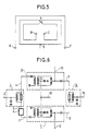
- the printed transformer with mid-point described below in relation to FIG. 4 is a transformer with two turns OB and OC, each half-winding then being reduced to one turn.
- This transformer corresponds to an optimal embodiment in which the flow created by each turn is identical to the flow created by the other, the OB and OC turns having the same perimeter and embracing the same surface, the diagram being indeed entirely symmetrical with respect to to a vertical axis passing on the one hand by the midpoint O and on the other hand by the crossing point of the turns, referenced D.
- the two half-windings have identical leakage coils.
- the crossing point of the turns can be achieved using metallized holes; the presence of metallization opposite the transformer does not affect its performance.
- the crossing point of the turns could also be achieved using a "chip" box mounted on the surface of zero resistance.
- the performances can be further optimized by reducing the space between turns (for example of the order of 15/100 mmm).
- a reduction in the width of the printed line for example to 15/100 mm) also makes it possible to reduce the dimensions of the transformer.
- This type of transformer will be used in distribution circuits 1, 14.
- a transformer used in mixers 8,11 is shown in Figure 5. It is deduced from the previous one by the addition of an additional turn EF at the periphery of the previous ones, this turn EF constituting the primary winding.
- the support of the modulation circuit includes an internal layer of insulation, it is then possible to have the transformers on each face without worrying about possible interactions.
- the modulation circuit according to the invention shown in FIG. 6 makes it possible to dispense with a DC component present in the modulation signals 10, 13. Indeed if these signals come from a circuit using an operational amplifier by example, a DC voltage superimposed on the useful signal is undesirable with respect to the two diodes of the mixer. It can be eliminated by using an isolation capacitor but if the frequencies used in the modulation signal are relatively low the capacitance of this capacitor will have to be large and, consequently, this component will be bulky.
- the solution adopted consists in applying a DC voltage 30 to the midpoints of the transformers of the mixers with the same value as that present in the modulation signals.
- the capacitors 32, 33 isolate the power supply producing this direct voltage with respect to the radiofrequency signals.
- This modulation circuit will advantageously be used in the demodulation circuit.
- the signal to be demodulated is injected in place of the output signal 15, the demodulated signals being received at the output of the mixers in place of the modulation signals 10, 13.
- the invention will find application in particular in radiotelephony in mobile stations where the baseband, phase 10 and quadrature 13 modulation signals will be applied to the mixers 8, 11.
Landscapes
- Engineering & Computer Science (AREA)
- Power Engineering (AREA)
- Amplitude Modulation (AREA)
- Stabilization Of Oscillater, Synchronisation, Frequency Synthesizers (AREA)
- Inductance-Capacitance Distribution Constants And Capacitance-Resistance Oscillators (AREA)
- Liquid Crystal (AREA)
- Amplifiers (AREA)
- Optical Communication System (AREA)
- Filters And Equalizers (AREA)
Applications Claiming Priority (2)
| Application Number | Priority Date | Filing Date | Title |
|---|---|---|---|
| FR8912335A FR2652210B1 (fr) | 1989-09-20 | 1989-09-20 | Circuit de modulation en phase et en amplitude. |
| FR8912335 | 1989-09-20 |
Publications (2)
| Publication Number | Publication Date |
|---|---|
| EP0418775A1 true EP0418775A1 (de) | 1991-03-27 |
| EP0418775B1 EP0418775B1 (de) | 1995-03-01 |
Family
ID=9385684
Family Applications (1)
| Application Number | Title | Priority Date | Filing Date |
|---|---|---|---|
| EP90117837A Expired - Lifetime EP0418775B1 (de) | 1989-09-20 | 1990-09-17 | Amplituden- und Phasenmodulator |
Country Status (9)
| Country | Link |
|---|---|
| EP (1) | EP0418775B1 (de) |
| AT (1) | ATE119335T1 (de) |
| AU (1) | AU633619B2 (de) |
| DE (1) | DE69017329T2 (de) |
| DK (1) | DK0418775T3 (de) |
| ES (1) | ES2070228T3 (de) |
| FI (1) | FI97000C (de) |
| FR (1) | FR2652210B1 (de) |
| NO (1) | NO176987C (de) |
Citations (3)
| Publication number | Priority date | Publication date | Assignee | Title |
|---|---|---|---|---|
| GB2084809A (en) * | 1980-10-01 | 1982-04-15 | Communications Patents Ltd | Printed circuit transformers |
| EP0324240A2 (de) * | 1988-01-15 | 1989-07-19 | Nortel Networks Corporation | Symmetrischer planarer Übertrager |
| EP0371157A1 (de) * | 1988-11-28 | 1990-06-06 | Siemens Aktiengesellschaft | Leitungstransformator |
Family Cites Families (1)
| Publication number | Priority date | Publication date | Assignee | Title |
|---|---|---|---|---|
| FR2644664B1 (fr) * | 1989-03-20 | 1996-04-26 | Alcatel Radiotelephone | Transformateur imprime sur circuit imprime, et circuit imprime diviseur de puissance comportant un tel transformateur |
-
1989
- 1989-09-20 FR FR8912335A patent/FR2652210B1/fr not_active Expired - Fee Related
-
1990
- 1990-09-05 AU AU62172/90A patent/AU633619B2/en not_active Ceased
- 1990-09-17 DE DE69017329T patent/DE69017329T2/de not_active Expired - Fee Related
- 1990-09-17 ES ES90117837T patent/ES2070228T3/es not_active Expired - Lifetime
- 1990-09-17 DK DK90117837.6T patent/DK0418775T3/da active
- 1990-09-17 AT AT90117837T patent/ATE119335T1/de not_active IP Right Cessation
- 1990-09-17 EP EP90117837A patent/EP0418775B1/de not_active Expired - Lifetime
- 1990-09-17 FI FI904572A patent/FI97000C/fi not_active IP Right Cessation
- 1990-09-18 NO NO904053A patent/NO176987C/no not_active IP Right Cessation
Patent Citations (3)
| Publication number | Priority date | Publication date | Assignee | Title |
|---|---|---|---|---|
| GB2084809A (en) * | 1980-10-01 | 1982-04-15 | Communications Patents Ltd | Printed circuit transformers |
| EP0324240A2 (de) * | 1988-01-15 | 1989-07-19 | Nortel Networks Corporation | Symmetrischer planarer Übertrager |
| EP0371157A1 (de) * | 1988-11-28 | 1990-06-06 | Siemens Aktiengesellschaft | Leitungstransformator |
Non-Patent Citations (1)
| Title |
|---|
| CONFERENCE PROCEEDINGS OF THE 7TH EUROPEAN MICROWAVE CONFERENCE, Copenhagen, 5-8 septembre 1977, pages 601-605, Sevenoaks, Kent, GB; B.R. HALLFORD: "2dB conversion loss mixer at 11 GHz using a PRM circuit" * |
Also Published As
| Publication number | Publication date |
|---|---|
| FI97000B (fi) | 1996-06-14 |
| NO176987B (no) | 1995-03-20 |
| NO904053D0 (no) | 1990-09-18 |
| FI97000C (fi) | 1996-09-25 |
| FI904572A0 (fi) | 1990-09-17 |
| FR2652210A1 (fr) | 1991-03-22 |
| DE69017329D1 (de) | 1995-04-06 |
| EP0418775B1 (de) | 1995-03-01 |
| AU633619B2 (en) | 1993-02-04 |
| ES2070228T3 (es) | 1995-06-01 |
| ATE119335T1 (de) | 1995-03-15 |
| DK0418775T3 (da) | 1995-05-22 |
| NO904053L (no) | 1991-03-21 |
| FR2652210B1 (fr) | 1995-06-16 |
| NO176987C (no) | 1995-06-28 |
| AU6217290A (en) | 1991-03-28 |
| DE69017329T2 (de) | 1995-06-29 |
Similar Documents
| Publication | Publication Date | Title |
|---|---|---|
| EP1097509A1 (de) | Vektormodulator | |
| EP0687059B1 (de) | Vorrichtung zur Beseitigung der Spiegelfrequenz eines in eine Zwischenfrequenz umgesetzten Basisbandsignals | |
| EP1081849A1 (de) | Zweiband-Verstärkungsschaltung und Hochfrequenempfangsteil | |
| EP0911969B1 (de) | Verstärkerschaltung mit Doppelverstärkung | |
| FR2669787A1 (fr) | Melangeur hyperfrequence symetrique. | |
| FR2771232A1 (fr) | Dispositif formant circuit haute frequence, en particulier un duplexeur a filtre a ondes acoustiques de surface et commutateur haute frequence | |
| EP1429458A2 (de) | Transformator mit Moduswechsel und Frequenzauswahl | |
| EP0795954B1 (de) | Vorrichtung mit einem Ring-Mischer | |
| FR2746547A1 (fr) | Antenne helice a alimentation large bande integree, et procedes de fabrication correspondants | |
| FR2792129A1 (fr) | Recepteur de signaux portable a plusieurs antennes | |
| EP0047686B1 (de) | Hybrider Mikrowellenmischer | |
| EP1178500B1 (de) | Induktive integrierte Struktur mit geteilten Werten auf einem Halbleitersubstrat | |
| EP0418775B1 (de) | Amplituden- und Phasenmodulator | |
| EP1417750B1 (de) | Mischerschaltung mit spiegelfrequenzunterdrückung , und deren verwendung in einem direktkonversionsempfänger | |
| FR2862158A1 (fr) | Balun distribue a rapport d'impedance non unitaire | |
| EP1148631B1 (de) | Frequenzumsetzer mit Unterdrückung der Spiegelfrequenzen | |
| FR2806534A1 (fr) | Dispositif a circuit non reciproque et appareil a circuit haute frequence l'incorporant | |
| US5811961A (en) | Amplitude and phase adjustment circuit | |
| FR3116400A1 (fr) | Module radiofréquence à point d’accès commun | |
| EP3692415B1 (de) | Hochfrequenz-oszillator und zugehörige quelle und vorrichtung | |
| EP0779703B1 (de) | Demodulatorschaltung für frequenzmoduliertes Signal in der Nähe einer Zwischenfrequenz | |
| FR2494917A1 (fr) | Coupleur hybride hyperfrequence a large bande et melangeur equilibre le comportant | |
| CA2063229C (en) | Binary phase shift keying modulation system and/or frequency multiplier | |
| FR2644664A1 (fr) | Transformateur imprime sur circuit imprime, et circuit imprime diviseur de puissance comportant un tel transformateur | |
| FR2785745A1 (fr) | Circuit haute frequence a dephasage variable |
Legal Events
| Date | Code | Title | Description |
|---|---|---|---|
| PUAI | Public reference made under article 153(3) epc to a published international application that has entered the european phase |
Free format text: ORIGINAL CODE: 0009012 |
|
| AK | Designated contracting states |
Kind code of ref document: A1 Designated state(s): AT BE CH DE DK ES FR GB GR IT LI LU NL SE |
|
| 17P | Request for examination filed |
Effective date: 19910924 |
|
| 17Q | First examination report despatched |
Effective date: 19940513 |
|
| RAP1 | Party data changed (applicant data changed or rights of an application transferred) |
Owner name: ALCATEL MOBILE COMMUNICATION FRANCE |
|
| GRAA | (expected) grant |
Free format text: ORIGINAL CODE: 0009210 |
|
| AK | Designated contracting states |
Kind code of ref document: B1 Designated state(s): AT BE CH DE DK ES FR GB GR IT LI LU NL SE |
|
| REF | Corresponds to: |
Ref document number: 119335 Country of ref document: AT Date of ref document: 19950315 Kind code of ref document: T |
|
| REF | Corresponds to: |
Ref document number: 69017329 Country of ref document: DE Date of ref document: 19950406 |
|
| ITF | It: translation for a ep patent filed | ||
| REG | Reference to a national code |
Ref country code: DK Ref legal event code: T3 |
|
| GBT | Gb: translation of ep patent filed (gb section 77(6)(a)/1977) |
Effective date: 19950425 |
|
| REG | Reference to a national code |
Ref country code: ES Ref legal event code: FG2A Ref document number: 2070228 Country of ref document: ES Kind code of ref document: T3 |
|
| REG | Reference to a national code |
Ref country code: GR Ref legal event code: FG4A Free format text: 3016295 |
|
| PLBE | No opposition filed within time limit |
Free format text: ORIGINAL CODE: 0009261 |
|
| STAA | Information on the status of an ep patent application or granted ep patent |
Free format text: STATUS: NO OPPOSITION FILED WITHIN TIME LIMIT |
|
| 26N | No opposition filed | ||
| PGFP | Annual fee paid to national office [announced via postgrant information from national office to epo] |
Ref country code: GB Payment date: 19990813 Year of fee payment: 10 |
|
| PGFP | Annual fee paid to national office [announced via postgrant information from national office to epo] |
Ref country code: CH Payment date: 19990816 Year of fee payment: 10 |
|
| PGFP | Annual fee paid to national office [announced via postgrant information from national office to epo] |
Ref country code: FR Payment date: 19990817 Year of fee payment: 10 |
|
| PGFP | Annual fee paid to national office [announced via postgrant information from national office to epo] |
Ref country code: NL Payment date: 19990819 Year of fee payment: 10 |
|
| PGFP | Annual fee paid to national office [announced via postgrant information from national office to epo] |
Ref country code: DE Payment date: 19990820 Year of fee payment: 10 |
|
| PGFP | Annual fee paid to national office [announced via postgrant information from national office to epo] |
Ref country code: SE Payment date: 19990823 Year of fee payment: 10 Ref country code: DK Payment date: 19990823 Year of fee payment: 10 |
|
| PGFP | Annual fee paid to national office [announced via postgrant information from national office to epo] |
Ref country code: AT Payment date: 19990824 Year of fee payment: 10 |
|
| PGFP | Annual fee paid to national office [announced via postgrant information from national office to epo] |
Ref country code: LU Payment date: 19990826 Year of fee payment: 10 |
|
| PGFP | Annual fee paid to national office [announced via postgrant information from national office to epo] |
Ref country code: BE Payment date: 19990827 Year of fee payment: 10 |
|
| PGFP | Annual fee paid to national office [announced via postgrant information from national office to epo] |
Ref country code: ES Payment date: 19990917 Year of fee payment: 10 |
|
| PGFP | Annual fee paid to national office [announced via postgrant information from national office to epo] |
Ref country code: GR Payment date: 19990927 Year of fee payment: 10 |
|
| PG25 | Lapsed in a contracting state [announced via postgrant information from national office to epo] |
Ref country code: LU Free format text: LAPSE BECAUSE OF NON-PAYMENT OF DUE FEES Effective date: 20000917 Ref country code: GB Free format text: LAPSE BECAUSE OF NON-PAYMENT OF DUE FEES Effective date: 20000917 Ref country code: DK Free format text: LAPSE BECAUSE OF NON-PAYMENT OF DUE FEES Effective date: 20000917 Ref country code: AT Free format text: LAPSE BECAUSE OF NON-PAYMENT OF DUE FEES Effective date: 20000917 |
|
| PG25 | Lapsed in a contracting state [announced via postgrant information from national office to epo] |
Ref country code: ES Free format text: LAPSE BECAUSE OF NON-PAYMENT OF DUE FEES Effective date: 20000918 |
|
| PG25 | Lapsed in a contracting state [announced via postgrant information from national office to epo] |
Ref country code: SE Free format text: THE PATENT HAS BEEN ANNULLED BY A DECISION OF A NATIONAL AUTHORITY Effective date: 20000929 |
|
| PG25 | Lapsed in a contracting state [announced via postgrant information from national office to epo] |
Ref country code: LI Free format text: LAPSE BECAUSE OF NON-PAYMENT OF DUE FEES Effective date: 20000930 Ref country code: GR Free format text: LAPSE BECAUSE OF NON-PAYMENT OF DUE FEES Effective date: 20000930 Ref country code: CH Free format text: LAPSE BECAUSE OF NON-PAYMENT OF DUE FEES Effective date: 20000930 Ref country code: BE Free format text: LAPSE BECAUSE OF NON-PAYMENT OF DUE FEES Effective date: 20000930 |
|
| BERE | Be: lapsed |
Owner name: ALCATEL MOBILE COMMUNICATION FRANCE Effective date: 20000930 |
|
| PG25 | Lapsed in a contracting state [announced via postgrant information from national office to epo] |
Ref country code: NL Free format text: LAPSE BECAUSE OF NON-PAYMENT OF DUE FEES Effective date: 20010401 |
|
| GBPC | Gb: european patent ceased through non-payment of renewal fee |
Effective date: 20000917 |
|
| REG | Reference to a national code |
Ref country code: CH Ref legal event code: PL |
|
| EUG | Se: european patent has lapsed |
Ref document number: 90117837.6 |
|
| REG | Reference to a national code |
Ref country code: DK Ref legal event code: EBP |
|
| PG25 | Lapsed in a contracting state [announced via postgrant information from national office to epo] |
Ref country code: FR Free format text: LAPSE BECAUSE OF NON-PAYMENT OF DUE FEES Effective date: 20010531 |
|
| NLV4 | Nl: lapsed or anulled due to non-payment of the annual fee |
Effective date: 20010401 |
|
| PG25 | Lapsed in a contracting state [announced via postgrant information from national office to epo] |
Ref country code: DE Free format text: LAPSE BECAUSE OF NON-PAYMENT OF DUE FEES Effective date: 20010601 |
|
| REG | Reference to a national code |
Ref country code: FR Ref legal event code: ST |
|
| REG | Reference to a national code |
Ref country code: ES Ref legal event code: FD2A Effective date: 20011011 |
|
| PG25 | Lapsed in a contracting state [announced via postgrant information from national office to epo] |
Ref country code: IT Free format text: LAPSE BECAUSE OF NON-PAYMENT OF DUE FEES Effective date: 20050917 |