EP0419128B1 - Transistor MOS en silicium dopé au germanium pour augmenter sa durée de vie - Google Patents
Transistor MOS en silicium dopé au germanium pour augmenter sa durée de vie Download PDFInfo
- Publication number
- EP0419128B1 EP0419128B1 EP90310018A EP90310018A EP0419128B1 EP 0419128 B1 EP0419128 B1 EP 0419128B1 EP 90310018 A EP90310018 A EP 90310018A EP 90310018 A EP90310018 A EP 90310018A EP 0419128 B1 EP0419128 B1 EP 0419128B1
- Authority
- EP
- European Patent Office
- Prior art keywords
- germanium
- region
- junction
- transistor
- drain
- Prior art date
- Legal status (The legal status is an assumption and is not a legal conclusion. Google has not performed a legal analysis and makes no representation as to the accuracy of the status listed.)
- Expired - Lifetime
Links
Images
Classifications
-
- H—ELECTRICITY
- H10—SEMICONDUCTOR DEVICES; ELECTRIC SOLID-STATE DEVICES NOT OTHERWISE PROVIDED FOR
- H10P—GENERIC PROCESSES OR APPARATUS FOR THE MANUFACTURE OR TREATMENT OF DEVICES COVERED BY CLASS H10
- H10P30/00—Ion implantation into wafers, substrates or parts of devices
- H10P30/20—Ion implantation into wafers, substrates or parts of devices into semiconductor materials, e.g. for doping
- H10P30/202—Ion implantation into wafers, substrates or parts of devices into semiconductor materials, e.g. for doping characterised by the semiconductor materials
- H10P30/204—Ion implantation into wafers, substrates or parts of devices into semiconductor materials, e.g. for doping characterised by the semiconductor materials into Group IV semiconductors
-
- H—ELECTRICITY
- H10—SEMICONDUCTOR DEVICES; ELECTRIC SOLID-STATE DEVICES NOT OTHERWISE PROVIDED FOR
- H10D—INORGANIC ELECTRIC SEMICONDUCTOR DEVICES
- H10D62/00—Semiconductor bodies, or regions thereof, of devices having potential barriers
- H10D62/10—Shapes, relative sizes or dispositions of the regions of the semiconductor bodies; Shapes of the semiconductor bodies
- H10D62/13—Semiconductor regions connected to electrodes carrying current to be rectified, amplified or switched, e.g. source or drain regions
- H10D62/149—Source or drain regions of field-effect devices
- H10D62/151—Source or drain regions of field-effect devices of IGFETs
-
- H—ELECTRICITY
- H10—SEMICONDUCTOR DEVICES; ELECTRIC SOLID-STATE DEVICES NOT OTHERWISE PROVIDED FOR
- H10D—INORGANIC ELECTRIC SEMICONDUCTOR DEVICES
- H10D62/00—Semiconductor bodies, or regions thereof, of devices having potential barriers
- H10D62/10—Shapes, relative sizes or dispositions of the regions of the semiconductor bodies; Shapes of the semiconductor bodies
- H10D62/17—Semiconductor regions connected to electrodes not carrying current to be rectified, amplified or switched, e.g. channel regions
- H10D62/213—Channel regions of field-effect devices
- H10D62/221—Channel regions of field-effect devices of FETs
- H10D62/235—Channel regions of field-effect devices of FETs of IGFETs
-
- H—ELECTRICITY
- H10—SEMICONDUCTOR DEVICES; ELECTRIC SOLID-STATE DEVICES NOT OTHERWISE PROVIDED FOR
- H10D—INORGANIC ELECTRIC SEMICONDUCTOR DEVICES
- H10D62/00—Semiconductor bodies, or regions thereof, of devices having potential barriers
- H10D62/80—Semiconductor bodies, or regions thereof, of devices having potential barriers characterised by the materials
- H10D62/83—Semiconductor bodies, or regions thereof, of devices having potential barriers characterised by the materials being Group IV materials, e.g. B-doped Si or undoped Ge
- H10D62/834—Semiconductor bodies, or regions thereof, of devices having potential barriers characterised by the materials being Group IV materials, e.g. B-doped Si or undoped Ge further characterised by the dopants
-
- H—ELECTRICITY
- H10—SEMICONDUCTOR DEVICES; ELECTRIC SOLID-STATE DEVICES NOT OTHERWISE PROVIDED FOR
- H10P—GENERIC PROCESSES OR APPARATUS FOR THE MANUFACTURE OR TREATMENT OF DEVICES COVERED BY CLASS H10
- H10P30/00—Ion implantation into wafers, substrates or parts of devices
- H10P30/20—Ion implantation into wafers, substrates or parts of devices into semiconductor materials, e.g. for doping
- H10P30/208—Ion implantation into wafers, substrates or parts of devices into semiconductor materials, e.g. for doping of electrically inactive species
Definitions
- This invention relates to semiconductor devices and more particularly to transistor device structures in integrated circuits and to methods for making such structures.
- Each such device subject to this degradation is incorporated in a semiconductor body, typically silicon; and the device comprises a p-n junction, formed by the interface of two regions of the semiconductor body, one of the regions having a relatively high concentration of (conductivity-type determining) donor or acceptor impurities, the other having a relatively low concentration of acceptor or donor impurities, respectively--i.e., a p+n or an n+p junction, respectively.
- the p-n junction intersects the surface of the body at a location where the body is coated with an insulating layer.
- Degradation is believed to be caused by damage produced in the insulating layer by "hot" (fast-moving) charge carriers which are created in the region of relatively low impurity concentration, particularly in the neighborhood of the intersection of the p-n junction with the surface of the body. Accordingly, because of the higher electric fields which are ordinarily present in smaller sized devices and which cause a more severe hot charge carrier problem, smaller sized devices tend to have lower operational lifetimes.
- LDD lightly doped drain
- the concentration of conductivity-type determining impurities is reduced in a neighborhood of the drain.
- unwanted added series resistance in the drain outside the transistor channel is unavoidable, whereby the switching speed of the transistor is undesirably reduced, especially when the added resistance is comparable to the resistance of the channel itself, as is the case where the channel length is approximately 0.5 micrometer or less.
- BiCMOS Bipolar Complementary MOS
- EP-A-0419256 which forms part of the state of the art by virtue of Article 54(3)EPC, discloses a MOSFET doped with carbon in the channel region at the interface with the gate oxide to suppress hot electron trapping.
- the concentration is in the range 1016 - 1020cm ⁇ 3.
- Patent Abstracts of Japan, vol.11, no.31 (E-475) (2478) 29th January 1987 (JP-A-61-198681) discloses a MOS device with Ne, Ar, Kr or Xe implanted into the portions of the source and drain regions adjacent to the channel, to prevent hot electrons from being trapped in the gate oxide layer.
- US-A-4837173 discloses implantation of Ge ions near the location of the source and drain regions at a dose of 1015cm ⁇ 2.
- this decrease in degradation is attributable--for example, in MOS transistors--to a prevention of the formation of hot charge carriers at or near the drain, or both, by virtue of scattering of the carriers by the germanium atoms. It is theorized that this scattering reduces the number of hot charge carriers that can penetrate to the insulating layer, where the hot carriers damage the insulating layer and degrade device performance. Because they are neutral, moreover, the added germanium atoms apparently do not significantly reduce the desirable mobility of charge carriers in the channel. However, it should be understood that the successful results obtained in this invention do not depend upon the correctness of any theory.
- any required relatively high temperature annealing of the neutral germanium region can be (but not necessarily) performed prior to implanting the conductivity-type determining impurity required to form the p-n junction (which thereafter generally requires a relatively low-temperature annealing).
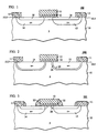
- an n-channel MOS transistor device structure 100 includes a portion 10 of a p-type silicon semiconductor body. Upon a top major surface 10.5 of this body 10 are located a relatively thick field oxide layer 11 and a thin gate oxide layer 12. Typically this gate oxide layer 12 has a thickness of about 12 nanometer or less for a channel length (gate oxide length) of about 0.8 micrometer or less. Upon the gate oxide layer 12 is located an n+ polycrystalline silicon gate electrode 13, as known in the art. Source and drain regions 14 and 15, respectively, are of n+ type conductivity, typically as formed by ion implantation of 80 keV arsenic followed by annealing, typically at about 900 degrees C for about 10 minutes. Metal or metal silicide source and drain electrodes (not shown) are typically attached to the respective surfaces of the source and drain regions, to complete the transistor device 100 and to supply it with electrical access to the rest of the circuit (not shown) integrated in the silicon body.
- the transistor device structure 100 is quite conventional.
- the device structure 100 further comprises a neutral impurity region in the form of a germanium doped region 16 formed prior to definition or formation of the gate electrode 13 but subsequent to the formation and patterning of the field oxide 11.
- the germanium region is formed, by example, by implantation with two doses of germanium ions, one having an energy of 25 keV and the other having an energy of 110 keV, using a standard source of germanium ions. Annealing is then performed at a temperature of about 950 degrees C, typically for approximately 30 to 60 minutes.
- this annealing of the germanium region which is performed advantageously for a longer time or at a higher temperature (or both) than the annealing of the arsenic at the source and drain, is performed prior to formation--as by the arsenic implantation--of the source and drain region. Because of the relatively low diffusivity of germanium in silicon, this annealing does not significantly change the depth of the germanium doped region 16.
- an MOS transistor device structure 200 has a similar structure to that of the previously described transistor device 100 except the germanium is implanted subsequent to the formation of the gate, and either prior or subsequent to the formation of the source and drain regions 14 and 15; and, in addition to the 25 keV and 110 keV doses of germanium used for the previously described structure 100, a dose of 160 keV (or higher) germanium is implanted into the body 10 in order to ensure that a portion of the germanium region 26 extends outside the metallurgical p-n junction 25 of the drain region 15 laterally into and substantially all the way across the width of the channel (at the surface 10.5 underneath the gate oxide layer 12), where it can suppress hot charge carrier formation.
- an annealing of the germanium region preferably is performed prior to source and drain implantation.
- an MOS transistor device structure 300 has a similar structure to that of the previously described device structure 200 except for the presence of a side-wall oxide (or other insulator) layer 32.
- the implantation of arsenic to form the source and drain regions is performed subsequent to side-wall oxide formation; whereas the implantation of the germanium to form the germanium doped region 36 is performed prior to side-wall oxide layer formation, in order to ensure that a portion of the germanium region 36 extends outside the drain region 15 laterally into (and across) the channel.
- Transistor devices of the kind shown in FIGS. 1,2, and 3 have been fabricated and successfully tested, and the implantations of germanium to concentration in the approximate range of 3x10¹⁷ to 1x10²⁰ (3E17 to 1E20) per cubic centimeter have resulted in significant improvements (reductions) in the rate of degradation of the transconductance. More specifically, to obtain the germanium concentration of 3E17 per cubic centimeter, a dose of 1E12 per square centimeter of 25 keV germanium ions plus a dose of 3E12 per square centimeter of 110 keV germanium ions (plus a dose of 3E12 per square centimeter of 160 keV germanium ions in the case of the structure 200) can be used.
- germanium concentration of 1E20 per cubic centimeter a dose of 3E14 per square centimeter of 25 keV germanium ions plus a dose of 1E15 per square centimeter of 110 keV germanium ions can be used. It should be noted that doses of germanium in an amount above about 3E19 per cubic centimeter produce amorphous silicon; doses below that amount produce damaged silicon. Higher germanium concentration than 1E20 per cubic centimeter may prove to be useful in conjunction with higher annealing temperatures. It should be noted, however, that experiments performed thus far on structures of the kind shown in FIG. 1 have indicated that the germanium concentration in this kind of structure (but not in structures like 200 and 300) should be limited to not more than 1E19 per cubic centimeter.
- the polysilicon gate can be a p+ polysilicon or a metal gate, instead of a n+ polysilicon gate.
- p-channel silicon MOS transistors similarly can benefit from neutral germanium regions in the neighborhood of the drain junction.
- both p-channel and n-channel transistor devices can be interconnected and integrated in the same silicon body, as known in the complementary MOS (CMOS) integrated circuit art, with either or both of these types of devices having the neutral germanium impurity regions described above, to reduce the rate of device degradation.
- CMOS complementary MOS
- MOS transistor devices of this invention can be interconnected and integrated with bipolar transistors in the same semiconductor body.
- a single annealing step can be used to repair simultaneously both the germanium and the arsenic damage at a temperature and for a time sufficient for repairing the damage due to the germanium implantation.
- the parameters of such a single annealing step must be carefully adjusted to ensure that in the device 200 the germanium region 26 extends beyond the metallurgical p-n junction 25 into the p-type silicon body 10 everywhere in a neighborhood of at least one-half the intersection of the metallurgical p-n junction 25 with the surface 10.5, such neighborhood thus extending laterally beyond the junction into the channel for a distance advantageously equal to at least approximately 0.01 micrometer.
- the neutral impurity region encompasses the regions of the devices where detrimental hot carriers are formed, particularly at or near (or both) an intersection of a p-n junction with a semiconductor surface.
Landscapes
- Insulated Gate Type Field-Effect Transistor (AREA)
- Metal-Oxide And Bipolar Metal-Oxide Semiconductor Integrated Circuits (AREA)
- Bipolar Transistors (AREA)
Claims (3)
- Un transistor MOS formé dans une région de dispositif d'un premier type de conductivité d'un substrat en silicium, ce transistor comprenant une région de drain (15) dans une région de surface de la région de dispositif, formant une jonction p-n avec la région de dispositif et ayant une concentration en impuretés supérieure à celle de la région de dispositif, un canal contigu à la région de drain, une partie (16, 26, 36) de la région de dispositif contenant des atomes de germanium, la concentration d'atomes de germanium dans cette partie étant au moins de 3 x 10¹⁷ atomes/cm³ et étant également au moins aussi élevée que la concentration en impuretés de la région de dispositif à l'intersection de la jonction p-n avec la surface du substrat, la partie précitée étant contiguë à au moins la moitié de l'intersection de la jonction p-n avec la surface (10.5) du substrat, et cette partie s'étendant latéralement au-delà de la région de drain et à l'intérieur du canal sur une distance d'au moins 0,01 »m.
- Le transistor de la revendication 1, dans lequel une couche isolante (11, 12) recouvre la surface du substrat à l'endroit auquel la jonction p-n la rencontre.
- Un circuit intégré comprenant le transistor spécifié dans la revendication 1 ou 2.
Applications Claiming Priority (2)
| Application Number | Priority Date | Filing Date | Title |
|---|---|---|---|
| US41106189A | 1989-09-22 | 1989-09-22 | |
| US411061 | 1989-09-22 |
Publications (2)
| Publication Number | Publication Date |
|---|---|
| EP0419128A1 EP0419128A1 (fr) | 1991-03-27 |
| EP0419128B1 true EP0419128B1 (fr) | 1995-04-19 |
Family
ID=23627399
Family Applications (1)
| Application Number | Title | Priority Date | Filing Date |
|---|---|---|---|
| EP90310018A Expired - Lifetime EP0419128B1 (fr) | 1989-09-22 | 1990-09-13 | Transistor MOS en silicium dopé au germanium pour augmenter sa durée de vie |
Country Status (5)
| Country | Link |
|---|---|
| US (1) | US5134447A (fr) |
| EP (1) | EP0419128B1 (fr) |
| JP (1) | JPH03119732A (fr) |
| DE (1) | DE69018744T2 (fr) |
| HK (1) | HK100396A (fr) |
Families Citing this family (27)
| Publication number | Priority date | Publication date | Assignee | Title |
|---|---|---|---|---|
| US5245208A (en) * | 1991-04-22 | 1993-09-14 | Mitsubishi Denki Kabushiki Kaisha | Semiconductor device and manufacturing method thereof |
| US5137838A (en) * | 1991-06-05 | 1992-08-11 | National Semiconductor Corporation | Method of fabricating P-buried layers for PNP devices |
| JPH0521762A (ja) * | 1991-07-10 | 1993-01-29 | Mitsubishi Electric Corp | 電界効果型トランジスタを備えた半導体装置およびその製造方法 |
| US5192712A (en) * | 1992-04-15 | 1993-03-09 | National Semiconductor Corporation | Control and moderation of aluminum in silicon using germanium and germanium with boron |
| DE4223914C2 (de) * | 1992-06-30 | 1996-01-25 | Fraunhofer Ges Forschung | Verfahren zum Herstellen eines vertikalen Leistungsbauelementes mit reduzierter Minoritätsträgerlebensdauer in dessen Driftstrecke |
| EP0622834A3 (fr) * | 1993-04-30 | 1998-02-11 | International Business Machines Corporation | Méthode pour prévenir le latch-up et améliorer la tension de claquage dans les MOSFET SOI |
| JP3830541B2 (ja) * | 1993-09-02 | 2006-10-04 | 株式会社ルネサステクノロジ | 半導体装置及びその製造方法 |
| US5514902A (en) * | 1993-09-16 | 1996-05-07 | Mitsubishi Denki Kabushiki Kaisha | Semiconductor device having MOS transistor |
| JP3361922B2 (ja) * | 1994-09-13 | 2003-01-07 | 株式会社東芝 | 半導体装置 |
| US6331458B1 (en) * | 1994-10-11 | 2001-12-18 | Advanced Micro Devices, Inc. | Active region implant methodology using indium to enhance short channel performance of a surface channel PMOS device |
| EP0717435A1 (fr) * | 1994-12-01 | 1996-06-19 | AT&T Corp. | Procédé de contrÔle de la diffusion de dopant dans une couche semiconductrice et couche semiconductrice ainsi formée |
| US5634001A (en) * | 1995-06-07 | 1997-05-27 | International Business Machines Corporation | Method to calculate hot-electron test voltage differential for assessing microprocessor reliability |
| US5650350A (en) * | 1995-08-11 | 1997-07-22 | Micron Technology, Inc. | Semiconductor processing method of forming a static random access memory cell and static random access memory cell |
| US5821147A (en) * | 1995-12-11 | 1998-10-13 | Lucent Technologies, Inc. | Integrated circuit fabrication |
| US5770485A (en) * | 1997-03-04 | 1998-06-23 | Advanced Micro Devices, Inc. | MOSFET device with an amorphized source and fabrication method thereof |
| US6225151B1 (en) | 1997-06-09 | 2001-05-01 | Advanced Micro Devices, Inc. | Nitrogen liner beneath transistor source/drain regions to retard dopant diffusion |
| EP0926739A1 (fr) | 1997-12-24 | 1999-06-30 | Texas Instruments Incorporated | Structure et procédé pour un transistor à effet de champ du type MIS |
| US6030863A (en) * | 1998-09-11 | 2000-02-29 | Taiwan Semiconductor Manufacturing Company | Germanium and arsenic double implanted pre-amorphization process for salicide technology |
| US6124627A (en) * | 1998-12-03 | 2000-09-26 | Texas Instruments Incorporated | Lateral MOSFET having a barrier between the source/drain region and the channel region using a heterostructure raised source/drain region |
| DE10030381B4 (de) * | 2000-06-21 | 2005-04-14 | eupec Europäische Gesellschaft für Leistungshalbleiter mbH & Co. KG | Leistungshalbleiterbauelement aufweisend einen Körper aus Halbleitermaterial mit Übergang zwischen zueinander entgegengesetzten Leiterfähigkeitstypen |
| US6777275B1 (en) * | 2000-11-15 | 2004-08-17 | Advanced Micro Devices, Inc. | Single anneal for dopant activation and silicide formation |
| US6638802B1 (en) * | 2002-06-20 | 2003-10-28 | Intel Corporation | Forming strained source drain junction field effect transistors |
| US20050104092A1 (en) * | 2003-11-19 | 2005-05-19 | International Business Machiness Corportion | Method of reducing dislocation-induced leakage in a strained-layer field-effect transistor |
| DE102005042827A1 (de) * | 2005-09-09 | 2007-03-22 | Atmel Germany Gmbh | Hochvolt-Feldeffekttransistor und Verfahren zur Herstellung eines Hochvolt-Feldeffekttransistors |
| DE102006019935B4 (de) | 2006-04-28 | 2011-01-13 | Advanced Micro Devices, Inc., Sunnyvale | SOI-Transistor mit reduziertem Körperpotential und ein Verfahren zur Herstellung |
| WO2007126807A1 (fr) * | 2006-04-28 | 2007-11-08 | Advanced Micro Devices, Inc. | Transistor soi à potentiel de corps réduit et son procédé de fabrication |
| US8101489B2 (en) * | 2008-01-28 | 2012-01-24 | Taiwan Semiconductor Manufacturing Company, Ltd. | Approach to reduce the contact resistance |
Citations (1)
| Publication number | Priority date | Publication date | Assignee | Title |
|---|---|---|---|---|
| EP0419256A1 (fr) * | 1989-09-21 | 1991-03-27 | Hewlett-Packard Company | Substrat MOSFET dopé au carbone pour la suppression des pièges par électrons chauds |
Family Cites Families (9)
| Publication number | Priority date | Publication date | Assignee | Title |
|---|---|---|---|---|
| US4636822A (en) * | 1984-08-27 | 1987-01-13 | International Business Machines Corporation | GaAs short channel lightly doped drain MESFET structure and fabrication |
| US4603471A (en) * | 1984-09-06 | 1986-08-05 | Fairchild Semiconductor Corporation | Method for making a CMOS circuit having a reduced tendency to latch by controlling the band-gap of source and drain regions |
| US4613882A (en) * | 1985-04-12 | 1986-09-23 | General Electric Company | Hybrid extended drain concept for reduced hot electron effect |
| US4680603A (en) * | 1985-04-12 | 1987-07-14 | General Electric Company | Graded extended drain concept for reduced hot electron effect |
| CA1216962A (fr) * | 1985-06-28 | 1987-01-20 | Hussein M. Naguib | Methode de fabrication de dispositifs mos |
| US4843023A (en) * | 1985-09-25 | 1989-06-27 | Hewlett-Packard Company | Process for forming lightly-doped-drain (LDD) without extra masking steps |
| US4837173A (en) * | 1987-07-13 | 1989-06-06 | Motorola, Inc. | N-channel MOS transistors having source/drain regions with germanium |
| JPH01112772A (ja) * | 1987-10-27 | 1989-05-01 | Fujitsu Ltd | Mis型半導体装置 |
| US4835112A (en) * | 1988-03-08 | 1989-05-30 | Motorola, Inc. | CMOS salicide process using germanium implantation |
-
1990
- 1990-08-27 US US07/574,564 patent/US5134447A/en not_active Expired - Lifetime
- 1990-09-13 EP EP90310018A patent/EP0419128B1/fr not_active Expired - Lifetime
- 1990-09-13 DE DE69018744T patent/DE69018744T2/de not_active Expired - Fee Related
- 1990-09-21 JP JP2250429A patent/JPH03119732A/ja active Pending
-
1996
- 1996-06-06 HK HK100396A patent/HK100396A/en unknown
Patent Citations (1)
| Publication number | Priority date | Publication date | Assignee | Title |
|---|---|---|---|---|
| EP0419256A1 (fr) * | 1989-09-21 | 1991-03-27 | Hewlett-Packard Company | Substrat MOSFET dopé au carbone pour la suppression des pièges par électrons chauds |
Also Published As
| Publication number | Publication date |
|---|---|
| JPH03119732A (ja) | 1991-05-22 |
| EP0419128A1 (fr) | 1991-03-27 |
| HK100396A (en) | 1996-06-14 |
| DE69018744T2 (de) | 1996-01-11 |
| US5134447A (en) | 1992-07-28 |
| DE69018744D1 (de) | 1995-05-24 |
Similar Documents
| Publication | Publication Date | Title |
|---|---|---|
| EP0419128B1 (fr) | Transistor MOS en silicium dopé au germanium pour augmenter sa durée de vie | |
| US5510279A (en) | Method of fabricating an asymmetric lightly doped drain transistor device | |
| JP4708563B2 (ja) | 薄くドープされたドレイントランジスタの有効なチャネル長さを減じる方法およびトランジスタを形成する方法 | |
| US5548143A (en) | Metal oxide semiconductor transistor and a method for manufacturing the same | |
| US6531739B2 (en) | Radiation-hardened silicon-on-insulator CMOS device, and method of making the same | |
| JP3164076B2 (ja) | 半導体装置の製造方法 | |
| US5041885A (en) | Surface field effect transistor with depressed source and/or drain areas for ULSI integrated devices | |
| KR20000069811A (ko) | 임계전압을 승압하는 웰 부스팅 | |
| US5536959A (en) | Self-aligned charge screen (SACS) field effect transistors and methods | |
| US6297098B1 (en) | Tilt-angle ion implant to improve junction breakdown in flash memory application | |
| EP0718892A2 (fr) | Dispositif semiconducteur avec transistor bipolaire à grille isolée et son procédé de fabrication | |
| US5021851A (en) | NMOS source/drain doping with both P and As | |
| US4839301A (en) | Blanket CMOS channel stop implant employing a combination of n-channel and p-channel punch-through implants | |
| US4851360A (en) | NMOS source/drain doping with both P and As | |
| US20040041170A1 (en) | Low dose super deep source/drain implant | |
| US7524710B2 (en) | Radiation-hardened silicon-on-insulator CMOS device, and method of making the same | |
| KR19980050121A (ko) | 트랜지스터 및 그 제조방법 | |
| US6476430B1 (en) | Integrated circuit | |
| US5963809A (en) | Asymmetrical MOSFET with gate pattern after source/drain formation | |
| JPS5893279A (ja) | 半導体装置の製造方法 | |
| US5399514A (en) | Method for manufacturing improved lightly doped diffusion (LDD) semiconductor device | |
| US5422510A (en) | MOS transistor with non-uniform channel dopant profile | |
| JP3144385B2 (ja) | 半導体装置とその製造方法 | |
| JPH04127537A (ja) | Mosfetの製造方法 | |
| USRE35827E (en) | Surface field effect transistor with depressed source and/or drain areas for ULSI integrated devices |
Legal Events
| Date | Code | Title | Description |
|---|---|---|---|
| PUAI | Public reference made under article 153(3) epc to a published international application that has entered the european phase |
Free format text: ORIGINAL CODE: 0009012 |
|
| AK | Designated contracting states |
Kind code of ref document: A1 Designated state(s): DE FR GB |
|
| 17P | Request for examination filed |
Effective date: 19910918 |
|
| 17Q | First examination report despatched |
Effective date: 19930730 |
|
| RAP3 | Party data changed (applicant data changed or rights of an application transferred) |
Owner name: AT&T CORP. |
|
| GRAA | (expected) grant |
Free format text: ORIGINAL CODE: 0009210 |
|
| AK | Designated contracting states |
Kind code of ref document: B1 Designated state(s): DE FR GB |
|
| ET | Fr: translation filed | ||
| REF | Corresponds to: |
Ref document number: 69018744 Country of ref document: DE Date of ref document: 19950524 |
|
| PGFP | Annual fee paid to national office [announced via postgrant information from national office to epo] |
Ref country code: GB Payment date: 19950717 Year of fee payment: 6 |
|
| PGFP | Annual fee paid to national office [announced via postgrant information from national office to epo] |
Ref country code: DE Payment date: 19950823 Year of fee payment: 6 |
|
| PGFP | Annual fee paid to national office [announced via postgrant information from national office to epo] |
Ref country code: FR Payment date: 19950824 Year of fee payment: 6 |
|
| PLBE | No opposition filed within time limit |
Free format text: ORIGINAL CODE: 0009261 |
|
| STAA | Information on the status of an ep patent application or granted ep patent |
Free format text: STATUS: NO OPPOSITION FILED WITHIN TIME LIMIT |
|
| 26N | No opposition filed | ||
| PG25 | Lapsed in a contracting state [announced via postgrant information from national office to epo] |
Ref country code: GB Effective date: 19960913 |
|
| PG25 | Lapsed in a contracting state [announced via postgrant information from national office to epo] |
Ref country code: FR Effective date: 19960930 |
|
| GBPC | Gb: european patent ceased through non-payment of renewal fee |
Effective date: 19960913 |
|
| PG25 | Lapsed in a contracting state [announced via postgrant information from national office to epo] |
Ref country code: DE Effective date: 19970603 |
|
| REG | Reference to a national code |
Ref country code: FR Ref legal event code: ST |
|
| REG | Reference to a national code |
Ref country code: FR Ref legal event code: ST |