EP0419200A2 - Verfahren zum Herstellen von Oxyd-Supraleitern - Google Patents
Verfahren zum Herstellen von Oxyd-Supraleitern Download PDFInfo
- Publication number
- EP0419200A2 EP0419200A2 EP90310180A EP90310180A EP0419200A2 EP 0419200 A2 EP0419200 A2 EP 0419200A2 EP 90310180 A EP90310180 A EP 90310180A EP 90310180 A EP90310180 A EP 90310180A EP 0419200 A2 EP0419200 A2 EP 0419200A2
- Authority
- EP
- European Patent Office
- Prior art keywords
- layer
- oxide superconductor
- substrate
- elements
- producing
- Prior art date
- Legal status (The legal status is an assumption and is not a legal conclusion. Google has not performed a legal analysis and makes no representation as to the accuracy of the status listed.)
- Withdrawn
Links
Images


Classifications
-
- H—ELECTRICITY
- H10—SEMICONDUCTOR DEVICES; ELECTRIC SOLID-STATE DEVICES NOT OTHERWISE PROVIDED FOR
- H10N—ELECTRIC SOLID-STATE DEVICES NOT OTHERWISE PROVIDED FOR
- H10N60/00—Superconducting devices
- H10N60/01—Manufacture or treatment
- H10N60/0268—Manufacture or treatment of devices comprising copper oxide
- H10N60/0296—Processes for depositing or forming copper oxide superconductor layers
- H10N60/0548—Processes for depositing or forming copper oxide superconductor layers by deposition and subsequent treatment, e.g. oxidation of pre-deposited material
-
- Y—GENERAL TAGGING OF NEW TECHNOLOGICAL DEVELOPMENTS; GENERAL TAGGING OF CROSS-SECTIONAL TECHNOLOGIES SPANNING OVER SEVERAL SECTIONS OF THE IPC; TECHNICAL SUBJECTS COVERED BY FORMER USPC CROSS-REFERENCE ART COLLECTIONS [XRACs] AND DIGESTS
- Y10—TECHNICAL SUBJECTS COVERED BY FORMER USPC
- Y10S—TECHNICAL SUBJECTS COVERED BY FORMER USPC CROSS-REFERENCE ART COLLECTIONS [XRACs] AND DIGESTS
- Y10S505/00—Superconductor technology: apparatus, material, process
- Y10S505/725—Process of making or treating high tc, above 30 k, superconducting shaped material, article, or device
- Y10S505/73—Vacuum treating or coating
- Y10S505/731—Sputter coating
-
- Y—GENERAL TAGGING OF NEW TECHNOLOGICAL DEVELOPMENTS; GENERAL TAGGING OF CROSS-SECTIONAL TECHNOLOGIES SPANNING OVER SEVERAL SECTIONS OF THE IPC; TECHNICAL SUBJECTS COVERED BY FORMER USPC CROSS-REFERENCE ART COLLECTIONS [XRACs] AND DIGESTS
- Y10—TECHNICAL SUBJECTS COVERED BY FORMER USPC
- Y10S—TECHNICAL SUBJECTS COVERED BY FORMER USPC CROSS-REFERENCE ART COLLECTIONS [XRACs] AND DIGESTS
- Y10S505/00—Superconductor technology: apparatus, material, process
- Y10S505/725—Process of making or treating high tc, above 30 k, superconducting shaped material, article, or device
- Y10S505/73—Vacuum treating or coating
- Y10S505/732—Evaporative coating with superconducting material
Definitions
- This invention relates to a method for producing an oxide superconductor, for example an A-Ce-Cu-O type oxide superconductor (wherein A is a lanthanoid element or rare earth element) or a Bi oxide superconductor.
- an oxide superconductor for example an A-Ce-Cu-O type oxide superconductor (wherein A is a lanthanoid element or rare earth element) or a Bi oxide superconductor.
- a metal or alloy superconductor to a device have been made. Nevertheless, since the critical temperature, Tc, is low, such a device could not be used in liquid helium. On the other hand, a oxide superconductor has a high Tc and has the ability to be used in liquid nitrogen.
- oxide superconductor a hole injection type oxide superconductor such as yttrium (Y) or bismuth (Bi) type and an electron injection type oxide superconductor such as Ln 2-X Ce X CuO 4-Y type are well known.
- a hole injection type oxide superconductor needs to be annealed in an oxidizing atmosphere.
- an electron injection type oxide superconductor needs to be annealed in a reducing atmosphere.
- oxide superconductor is applied to an interconnection or wiring layer in an electrical device.
- a conventional oxide superconductor is produced by a sputtering method usually using a sintered mass as a target.
- a sintered mass containing the elements Ln (lanthanide), Ce ( cerium), Cu (copper) etc. is produced and sputtering is effected using the sintered bulk as a target whereby the superconductor film is formed on a required substrate.
- the film composition has readily varying phases such as CeO2 , Ln2O7 , etc., other than superconducting Ln 2-X Ce X CuO 4-Y and the superconducting properties of the obtained superconductor are deteriorated as a result.
- a Bi type oxide superconductor such as (Bi 2-X-Y Pb X Sb Y )Sr2Ca2Cu3O10
- a sintered mass made of Bi2O3 , PbO, Sb2O3 , SrCO3 , CaCO3 and CuO is used as a target to carry out a sputtering method.
- Sb is present in such a manner that it is solid dissolved in Bi. Addition of a required or constant amount of Sb is very difficult because the additional amount of Sb is small and Sb is easily aggregated. Thus, a reproducible superconductor composition cannot be obtained and Sb2O3 or an unidentified phase other than a (Bi 2-X-Y Pb X Sb Y )Sr2Ca2Cu3O10 phase was found.
- a method for producing an oxide superconductor comprising the steps of: forming on a substrate a layer of (n-m) elements wherein n represents the number of elements which is to form an oxide superconductor and m is an integer less than n such that m ⁇ 1; and immersing the substrate with said layer thereon in a solution containing a supplementary element which is a said oxide superconductor composing element not present in said layer.
- the layer is of A-Cu-O type (wherein A is lanthanoid element or a rare earth element) compound.
- A is a lanthanoid element selected from Ln, Nd, Sm, Pr and Y.
- a Ce-containing solution is preferably selected from cerium nitrate Ce(NO3)3, cerium acetate Ce(CH3COO)3, cerium carbonate Ce2(CO3)3 and cerium oxalate Ce2(C2O4)3 solutions.
- this invention provides a method for producing an oxide superconductor comprising the steps of: forming a layer of oxide superconductor-forming elements on a substrate and immersing said substrate with said layer formed thereon in a solution containing a supplementary element which is at least one of elements composing said oxide superconductor.
- the layer consists of (Bi 2-X Pb X )Sr2Ca2Cu3O10.
- an Sb-containing solution is preferably selected from, antimonyl chloride (SbOCl), antimony trichloride SbCl3 and chloroantimonic acid (H3SbCl6).
- the present invention by saturating a layer of main oxide superconductor composing elements with a supplementary element by immersing the layer in a solution containing the supplementary element, the supplementary element is uniformly added to the layer so that an oxide superconductor can be obtained. Thus, the occurrence of another phase which is not a superconductor phase is prevented.
- the added amount of the supplementary element can be easily controlled.
- Nd2O3 powder and CuO powder raw materials are mixed and milled by using a ball mill (step 1).
- the mixed powder is calcined in an Ar(argon) atmosphere at a temperature of 850 to 950°C for 10 to 30 hours (step 2).
- the calcined product is subjected to pressing (step 3) and to sintering at a temperature of 980 to 1200°C for 10 to 30 hours in an Ar(argon) atmosphere (step 4) so that a sintered target mass of Nd2O3 and CuO is formed.
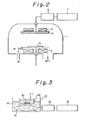
- sputtering is carried out by using the sputtering device shown in Fig. 2 (step 5).
- a target 4 and a substrate 5 are provided in a chamber 1, 2 and 3 denoting magnets and 6 and 7 denoting a matching box and rf power source respectively.
- Ar gas is supplied into the chamber 1.
- MgO or PSZ (partially stabilized zirconia) substrate 5 heated at a temperature of 500 to 700°C is used.
- the sputtering is carried out in an Ar(argon) atmosphere of 0.1 torr so that an approximately 5000 ⁇ thick Nd2CuO4 thin film is deposited on the substrate.
- the substrate 10 obtained is immersed in a Ce-containing solution 11 in a vessel 20.
- the vessel is floated on a body 12 of hot water in a constant temperature bath 13.
- the hot water is heated by a heater 14 connected to a thermocouple 15, and power source 16.
- Nd2CuO4 is saturated with Ce (step 6).
- cerium nitrate (Ce(NO3)3) was used as dissolved Ce compound in the Ce-containing solution.
- Ethyl alcohol (C2H5OH) was used as solvent.
- 0.4 g of cerium nitrate was added to 100 g of ethyl alcohol.
- the temperature of the constant temperature bath 13 was kept at 60°C.
- the Ce saturation procedure was carried out for 15 hours.
- the amount of Ce added to the Nd2CuO4 thin film can be controlled by controlling the concentration and the temperature of the Ce solution and the time saturation of Ce is allowed to continue for.
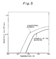
- the zero resistance temperature Tc is 5 to 15K, while on the other hand, the zero resistance temperature Tc of a Nd 2-X Ce X CuO 4-y superconductor thin film produced by the inventive process is 40K which is very much higher. Thus the superconductor property was improved.
- a mixed powder of 7 g of Bi2O3, 17 g of SrCO3, 25 g of CaCO3, 19 g of CuO and 4 g of PbO is milled using a ball mill (step 1). Subsequently, the mixed powder is calcined in air or an oxygen atmosphere at a temperature of 800 to 880°C for 10 to 30 hours (step 2).
- the calcined product is subjected to pressing (step 3) and to sintering at a temperature of 830 to 910°C for 10 to 30 hours in air or an oxygen atmosphere (step 4) so that a sintered target mass made of the product obtained is formed.
- sputtering is carried out by using the sputtering device shown in Fig. 2 (step 5).
- MgO or PSZ substrate 5 heated to a temperature of 500 to 700°C is used.
- the sputtering is carried out in an oxygen atmosphere of 0.1 torr so that an approximately 5000 ⁇ thick (Bi 2-X Pb X )Sr2Ca2Cu3O10 thin film is deposited on the substrate.
- the coated substrate obtained is immersed in a Sb-containing solution to saturate the coating with Sb as shown in Fig. 3.
- SbOCl antimonyl chloride
- 100 g of water added to 95 g (0.4 mol) of SbCl3 may be used.
- the temperature of the constant temperature bath was kept at 50°C.
- the Sb saturation procedure was carried out for 10 hours.
- a method for producing an oxide superconductor comprising the steps of forming on a substrate a layer of elements which is deficient in respect of one element for producing an oxide superconductor from said elements and immersing said substrate with layer formed thereon in a solution containing at leat one supplementary element required for producing said oxide superconductor.
Landscapes
- Engineering & Computer Science (AREA)
- Manufacturing & Machinery (AREA)
- Inorganic Compounds Of Heavy Metals (AREA)
- Superconductor Devices And Manufacturing Methods Thereof (AREA)
Applications Claiming Priority (4)
| Application Number | Priority Date | Filing Date | Title |
|---|---|---|---|
| JP241573/89 | 1989-09-18 | ||
| JP1241573A JPH03104872A (ja) | 1989-09-18 | 1989-09-18 | 酸化物超伝導体の製造方法 |
| JP2016212A JPH03223102A (ja) | 1990-01-29 | 1990-01-29 | 酸化物超伝導体の製造方法 |
| JP16212/90 | 1990-01-29 |
Publications (2)
| Publication Number | Publication Date |
|---|---|
| EP0419200A2 true EP0419200A2 (de) | 1991-03-27 |
| EP0419200A3 EP0419200A3 (en) | 1991-07-31 |
Family
ID=26352485
Family Applications (1)
| Application Number | Title | Priority Date | Filing Date |
|---|---|---|---|
| EP19900310180 Withdrawn EP0419200A3 (en) | 1989-09-18 | 1990-09-18 | Method for producing oxide superconductors |
Country Status (2)
| Country | Link |
|---|---|
| US (1) | US5110791A (de) |
| EP (1) | EP0419200A3 (de) |
Families Citing this family (1)
| Publication number | Priority date | Publication date | Assignee | Title |
|---|---|---|---|---|
| CA2074896C (en) * | 1992-07-29 | 2002-07-30 | Linh Ngo Phong | Process for making cuo superconductors |
Family Cites Families (4)
| Publication number | Priority date | Publication date | Assignee | Title |
|---|---|---|---|---|
| DE3850800T2 (de) * | 1987-04-13 | 1994-11-17 | Hitachi Ltd | Supraleitendes Material und Verfahren zu dessen Herstellung. |
| JPS63281321A (ja) * | 1987-05-14 | 1988-11-17 | Nippon Telegr & Teleph Corp <Ntt> | 酸化物超伝導材料の線材化方法 |
| DE3744145A1 (de) * | 1987-12-24 | 1989-07-06 | Asea Brown Boveri | Supraleiter und verfahren zu seiner herstellung |
| EP0362000B1 (de) * | 1988-08-30 | 1993-12-15 | Sumitomo Electric Industries, Ltd. | Verfahren zum Herstellen eines Oxid-Supraleiters vom Bismut-Typ |
-
1990
- 1990-09-18 EP EP19900310180 patent/EP0419200A3/en not_active Withdrawn
- 1990-09-18 US US07/584,345 patent/US5110791A/en not_active Expired - Fee Related
Non-Patent Citations (3)
| Title |
|---|
| APPLIED PHYSICS LETTERS, vol. 53, no. 4, 25th July 1988, pages 327-328, New York, US; A. MOGRO-CAMPERO et al.: "Superconducting thin films of Bi-Ca-Sr-Cu-O by sequential evaporation" * |
| NATURE, vol. 337, no. 6205, January 1989, pages 345-347, Basingstoke, GB; Y. TOKURA et al.: "A superconducting copper oxide compound with electrons as the charge carriers" * |
| PHYSICA C, vol. 158, no. 1-2, 1st April 1989, pages 97-101, Amsterdam, NL; S.X. DOU et al.: "Effect of Sb substitution on Tc in Bi-Pb-Sr-Ca-Cu-O systems" * |
Also Published As
| Publication number | Publication date |
|---|---|
| EP0419200A3 (en) | 1991-07-31 |
| US5110791A (en) | 1992-05-05 |
Similar Documents
| Publication | Publication Date | Title |
|---|---|---|
| JP2711253B2 (ja) | 超伝導膜及びその形成方法 | |
| EP0292958A2 (de) | Verfahren zur Herstellung einer dünnen Schicht aus supraleitendem Mischoxid | |
| EP0330214B2 (de) | Oxidischer Hochtemperatur-Supraleiter und Verfahren zu seiner Herstellung | |
| US4929595A (en) | Superconducting thin film fabrication | |
| EP0419200A2 (de) | Verfahren zum Herstellen von Oxyd-Supraleitern | |
| EP0358545B1 (de) | Prozess zur Herstellung thalliumartiger supraleitender Dünnfilme | |
| AU595142B2 (en) | Method of making a body, and article comprising the body | |
| US4929598A (en) | Oxygen plasma treatment of yttrium barium copper oxide | |
| EP0357500B1 (de) | Verfahren zum Herstellen einer supraleitenden Dünnschicht vom Wismut-Typ | |
| EP0347336A2 (de) | Verfahren zur Abscheidung einer dünnen Supraleiterschicht | |
| JP2817048B2 (ja) | スクリーン印刷によるBi−Sr−Ca−Cu−O系超伝導膜の製造方法 | |
| EP0344406B1 (de) | Tl-Kupferoxid-Supraleiter | |
| US5439878A (en) | Method for preparing copper oxide superconductor containing carbonate radicals | |
| US5104850A (en) | Preparation of high temperature superconducting coated wires by dipping and post annealing | |
| JP2832002B2 (ja) | Bi−Sr−Ca−Ci−O系超伝導薄膜の製造方法 | |
| JP3058515B2 (ja) | 超電導ジョセフソン素子およびその製法 | |
| KR0174382B1 (ko) | 고온 초전도 박막의 제조방법 | |
| EP0396478A2 (de) | Prozesse zur Bildung leitender Schichten und damit gebildete Artikel | |
| WO1988005604A1 (en) | Superconductors and method for manufacturing thereof | |
| JP2589087B2 (ja) | 超電導薄膜の製造方法 | |
| EP0334093A2 (de) | Halbzeug mit leitender Schicht und Verfahren zu seiner Herstellung | |
| JP2601892B2 (ja) | T▲l▼系超電導体配線パタ−ンの製造法 | |
| JPH01125878A (ja) | 薄膜多層超電導体 | |
| KR0157625B1 (ko) | Bi확산에 의한 고온 초전도 박막의 제조방법 | |
| EP0440411A2 (de) | Supraleitendes Oxid |
Legal Events
| Date | Code | Title | Description |
|---|---|---|---|
| PUAI | Public reference made under article 153(3) epc to a published international application that has entered the european phase |
Free format text: ORIGINAL CODE: 0009012 |
|
| AK | Designated contracting states |
Kind code of ref document: A2 Designated state(s): DE FR GB |
|
| PUAL | Search report despatched |
Free format text: ORIGINAL CODE: 0009013 |
|
| AK | Designated contracting states |
Kind code of ref document: A3 Designated state(s): DE FR GB |
|
| 17P | Request for examination filed |
Effective date: 19920122 |
|
| 17Q | First examination report despatched |
Effective date: 19931209 |
|
| STAA | Information on the status of an ep patent application or granted ep patent |
Free format text: STATUS: THE APPLICATION IS DEEMED TO BE WITHDRAWN |
|
| 18D | Application deemed to be withdrawn |
Effective date: 19940420 |