EP0419996B1 - Lötvorrichtung zum Auflöten von Bauelementen auf Leiterplatten - Google Patents
Lötvorrichtung zum Auflöten von Bauelementen auf Leiterplatten Download PDFInfo
- Publication number
- EP0419996B1 EP0419996B1 EP90117874A EP90117874A EP0419996B1 EP 0419996 B1 EP0419996 B1 EP 0419996B1 EP 90117874 A EP90117874 A EP 90117874A EP 90117874 A EP90117874 A EP 90117874A EP 0419996 B1 EP0419996 B1 EP 0419996B1
- Authority
- EP
- European Patent Office
- Prior art keywords
- soldering
- suction pipette
- components
- deformable material
- elastically deformable
- Prior art date
- Legal status (The legal status is an assumption and is not a legal conclusion. Google has not performed a legal analysis and makes no representation as to the accuracy of the status listed.)
- Expired - Lifetime
Links
Images
Classifications
-
- H—ELECTRICITY
- H05—ELECTRIC TECHNIQUES NOT OTHERWISE PROVIDED FOR
- H05K—PRINTED CIRCUITS; CASINGS OR CONSTRUCTIONAL DETAILS OF ELECTRIC APPARATUS; MANUFACTURE OF ASSEMBLAGES OF ELECTRICAL COMPONENTS
- H05K13/00—Apparatus or processes specially adapted for manufacturing or adjusting assemblages of electric components
- H05K13/04—Mounting of components, e.g. of leadless components
- H05K13/046—Surface mounting
- H05K13/0465—Surface mounting by soldering
-
- B—PERFORMING OPERATIONS; TRANSPORTING
- B23—MACHINE TOOLS; METAL-WORKING NOT OTHERWISE PROVIDED FOR
- B23K—SOLDERING OR UNSOLDERING; WELDING; CLADDING OR PLATING BY SOLDERING OR WELDING; CUTTING BY APPLYING HEAT LOCALLY, e.g. FLAME CUTTING; WORKING BY LASER BEAM
- B23K3/00—Tools, devices or special appurtenances for soldering, e.g. brazing, or unsoldering, not specially adapted for particular methods
- B23K3/04—Heating appliances
- B23K3/047—Heating appliances electric
- B23K3/0471—Heating appliances electric using resistance rod or bar, e.g. carbon silica
-
- H—ELECTRICITY
- H05—ELECTRIC TECHNIQUES NOT OTHERWISE PROVIDED FOR
- H05K—PRINTED CIRCUITS; CASINGS OR CONSTRUCTIONAL DETAILS OF ELECTRIC APPARATUS; MANUFACTURE OF ASSEMBLAGES OF ELECTRICAL COMPONENTS
- H05K3/00—Apparatus or processes for manufacturing printed circuits
- H05K3/30—Assembling printed circuits with electric components, e.g. with resistors
- H05K3/32—Assembling printed circuits with electric components, e.g. with resistors electrically connecting electric components or wires to printed circuits
- H05K3/34—Assembling printed circuits with electric components, e.g. with resistors electrically connecting electric components or wires to printed circuits by soldering
- H05K3/341—Surface mounted components
- H05K3/3421—Leaded components
-
- H—ELECTRICITY
- H05—ELECTRIC TECHNIQUES NOT OTHERWISE PROVIDED FOR
- H05K—PRINTED CIRCUITS; CASINGS OR CONSTRUCTIONAL DETAILS OF ELECTRIC APPARATUS; MANUFACTURE OF ASSEMBLAGES OF ELECTRICAL COMPONENTS
- H05K2203/00—Indexing scheme relating to apparatus or processes for manufacturing printed circuits covered by H05K3/00
- H05K2203/01—Tools for processing; Objects used during processing
- H05K2203/0195—Tool for a process not provided for in H05K3/00, e.g. tool for handling objects using suction, for deforming objects, for applying local pressure
-
- H—ELECTRICITY
- H05—ELECTRIC TECHNIQUES NOT OTHERWISE PROVIDED FOR
- H05K—PRINTED CIRCUITS; CASINGS OR CONSTRUCTIONAL DETAILS OF ELECTRIC APPARATUS; MANUFACTURE OF ASSEMBLAGES OF ELECTRICAL COMPONENTS
- H05K2203/00—Indexing scheme relating to apparatus or processes for manufacturing printed circuits covered by H05K3/00
- H05K2203/02—Details related to mechanical or acoustic processing, e.g. drilling, punching, cutting, using ultrasound
- H05K2203/0278—Flat pressure, e.g. for connecting terminals with anisotropic conductive adhesive
-
- H—ELECTRICITY
- H05—ELECTRIC TECHNIQUES NOT OTHERWISE PROVIDED FOR
- H05K—PRINTED CIRCUITS; CASINGS OR CONSTRUCTIONAL DETAILS OF ELECTRIC APPARATUS; MANUFACTURE OF ASSEMBLAGES OF ELECTRICAL COMPONENTS
- H05K2203/00—Indexing scheme relating to apparatus or processes for manufacturing printed circuits covered by H05K3/00
- H05K2203/08—Treatments involving gases
- H05K2203/082—Suction, e.g. for holding solder balls or components
-
- H—ELECTRICITY
- H05—ELECTRIC TECHNIQUES NOT OTHERWISE PROVIDED FOR
- H05K—PRINTED CIRCUITS; CASINGS OR CONSTRUCTIONAL DETAILS OF ELECTRIC APPARATUS; MANUFACTURE OF ASSEMBLAGES OF ELECTRICAL COMPONENTS
- H05K3/00—Apparatus or processes for manufacturing printed circuits
- H05K3/30—Assembling printed circuits with electric components, e.g. with resistors
- H05K3/303—Assembling printed circuits with electric components, e.g. with resistors with surface mounted components
-
- Y—GENERAL TAGGING OF NEW TECHNOLOGICAL DEVELOPMENTS; GENERAL TAGGING OF CROSS-SECTIONAL TECHNOLOGIES SPANNING OVER SEVERAL SECTIONS OF THE IPC; TECHNICAL SUBJECTS COVERED BY FORMER USPC CROSS-REFERENCE ART COLLECTIONS [XRACs] AND DIGESTS
- Y02—TECHNOLOGIES OR APPLICATIONS FOR MITIGATION OR ADAPTATION AGAINST CLIMATE CHANGE
- Y02P—CLIMATE CHANGE MITIGATION TECHNOLOGIES IN THE PRODUCTION OR PROCESSING OF GOODS
- Y02P70/00—Climate change mitigation technologies in the production process for final industrial or consumer products
- Y02P70/50—Manufacturing or production processes characterised by the final manufactured product
Definitions
- the invention relates to a soldering device for soldering components on printed circuit boards, with at least two clip electrodes that can be heated by electrical resistance heat and with a suction pipette arranged centrally between the clip electrodes for picking up, transporting and placing the components on the assigned solder points.
- Soldering devices with two clamp electrodes lying opposite one another in parallel or with four clamp electrodes lying opposite one another in pairs are used in particular for the soldering of multi-pole electronic components such as micropacks, flat packs and the like, the resistance heating of the clamp electrodes generally being carried out by means of current pulses.
- the connecting legs of the components and the conductor tracks or connecting pads of the printed circuit boards should be ensured both before the soldering process and during the entire duration of the soldering process.
- Automatic placement machines are used for the automatic assembly of circuit boards with surface-solderable components, which work according to the so-called pick & place principle.
- a placement head moves over the supply modules of the components and the printed circuit board arranged in the assembly area.
- This pick-up device picks up the components from the supply modules, centers them and, if necessary, rotates them into the correct installation position and places them on the printed circuit board in the intended placement position.
- the suction pipette can be used both before the soldering process and during the entire duration of the soldering process, the component with a limited force to press against the solder joint on the circuit board.
- a soldering device of the type mentioned at the beginning is known from ELECTRONIC PACKAGING AND PRODUCTION Vol. 28, No. 2, February 1988, Newton, Mass., USA, page 14 "Soldering machines take on quad flat pack".
- the suction pipette and the ironing electrodes With the suction pipette and the ironing electrodes, forces are exerted on the component independently of one another during the soldering process.
- the suction pipette holds the component in place with a force of 1.1 to 1.7 N, while the clamp electrodes bend the connecting legs of the component bent with a force of 2.8 N.
- GB-A-2 167 038 it is known to pick up components with a suction pipette and then to press them firmly into the adhesive applied to a printed circuit board via the suction pipette with a predetermined force.
- the suction pipette is provided with an elastic tip.
- Desoldering devices equipped with suction pipettes are known from EP-A-0 121 910 and GB-A-2 162 904. With these desoldering devices, the connections of electronic components are heated in such a way that the solder connecting the connections with a carrier plate melts and the components can be removed with the aid of the suction pipettes.
- the ends of the suction pipettes carry suction cups, which, thanks to their elastic design and bell-shaped enlargement, enable a high lifting force.
- the invention has for its object to provide a soldering device of the type mentioned, in which the suction pipette used for receiving, transporting and placing the components can also be used when the components are skewed on the circuit board to press the components onto the solder joint.
- the suction pipette consists of an elastically deformable material at least in its opening area facing the component.
- This resiliently deformable material then enables the suction pipette to be adapted to an inclined position of the component in a manner similar to a spherical bearing, this adaptation also leading to a certain compensation of the pressure exerted on the connecting legs. If the original skewed position of the component is then eliminated during the soldering process by the pressure exerted by the clip electrodes or by the melting of the connection pads, the elastically deformable material of the suction pipette can in this case adapt to the new position of the component.
- the elastically deformable material forms an annular circumferential lip in the opening area of the suction pipette facing the component.
- the rigid sleeve of the suction pipette carries a pipette insert made of the elastically deformable material.
- the elastic adaptation can be approximated even better to the effect of a corresponding spherical bearing.
- Hard rubber or plastic is preferably provided as the elastically deformable material.
- the choice of material must always be coordinated with the properties of the respective components.
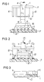
- Fig. 1 shows in a highly simplified schematic representation the basic principle of a soldering device according to the invention, wherein the parts such as power supply lines and the like which are not necessary for understanding the invention have been omitted.
- the soldering device shown has four U-shaped bracket electrodes attached to a soldering bracket holder LH, two bracket electrodes B1 and two bracket electrodes B2 being aligned parallel to one another in such a way that the working surfaces on the underside of the bracket electrodes B1 and B2 have a rectangular shape which is not closed in the end regions or form a square frame.
- the dimensions of this frame are matched to the shape and position of the connection legs A of a component BE to be soldered onto the connection pads AP of a printed circuit board LP.
- the components BE are removed from a magazine or from a feed module with the suction pipette S of a placement head (not shown in the drawing) and placed on the predetermined soldering point on the printed circuit board Lp.
- the structure and mode of operation of a placement head equipped with a suction pipette can be seen, for example, from US Pat. No. 4,135,630.
- the double-bent connection pins A should come into contact with the connection pads AP. Due to an angular misalignment of the circuit board Lp, by warping of the circuit board Lp, by different heights of the connection pads AP, by differently curved connection pins A or by similar causes, an inclined position of the component BE relative to the circuit board LP can be exaggerated in FIG. 1. If the suction pipette S is now used in such an inclined position to press the component BE against the printed circuit board LP before the soldering process and for the entire duration of the soldering process with a limited force F1 of, for example, 0.1 N to 0.5 N.
- a completely rigid design of the suction pipette S leads to an undesirable one-sided loading of the component BE and the terminal legs A seated prematurely on the assigned connection pads AP.
- a pipette insert PE made of an elastically deformable material such as hard rubber, silicone rubber or the like is accommodated in the lower end of the rigid, metallic sleeve H of the suction pipette S.
- this pipette insert PE adapts to the inclined position of the component BE in a manner similar to a spherical bearing and thus also brings about a certain compensation of the one-sided loading of Component BE and connection leg A.
- This elastic compensation is additionally reinforced by the annular lip L which can be seen in FIG. 3.
- the soldering bracket holder LH is moved downward, the working surfaces of the bracket electrodes B1 and B2 pressing the connection pins A with a force F2 of, for example, 40 N against the assigned connection pads AP .
- the force F1 exerted on the component BE via the suction pipette S is also maintained.
- the soldering of the solder of the connection pads AP is then carried out by a corresponding electrical resistance heating of the bracket electrodes B1 and B2, the original skew of the component BE being completely eliminated at the latest after this melting. It can be seen that the pipette insert PE also adapts to this new, now correct position of the component BE.
- the soldering bracket holder LH can be raised to form a defined solder layer between the connection pins A and the associated connection pads AP, and the component BE can be withdrawn upwards by a defined distance of, for example, 10 micrometers, by raising the suction pipette S.
- an articulated suspension of the soldering iron holder LH with a center of rotation and compensation located centrally in the plane between the working surfaces of the ironing electrodes B1 and B2 before the soldering process and for the entire duration of the soldering process ensures that there is always safe contact between the working surfaces, the connection leg A and the connection pads AP can be guaranteed.
- Such an articulated suspension of a soldering iron holder is shown and described, for example, in the earlier patent application P 39 005 20.8.
Landscapes
- Engineering & Computer Science (AREA)
- Manufacturing & Machinery (AREA)
- Microelectronics & Electronic Packaging (AREA)
- Mechanical Engineering (AREA)
- Electric Connection Of Electric Components To Printed Circuits (AREA)
- Manufacturing Of Electrical Connectors (AREA)
Description
- Die Erfindung betrifft eine Lötvorrichtung zum Auflöten von Bauelementen auf Leiterplatten, mit mindestens zwei durch elektrische Widerstandswärme erhitzbaren Bügelelektroden und mit einer mittig zwischen den Bügelelektroden angeordneten Saugpipette zum Aufnehmen, Transportieren und Aufsetzen der Bauelemente auf die zugeordneten Lötstellen.
- Lötvorrichtungen mit zwei parallel einander gegenüberliegenden Bügelelektroden oder mit vier paarweise einander gegenüberliegenden Bügelelektroden werden insbesondere für das Auflöten hochpoliger elektronischer Bauelemente wie Mikropacks, Flatpacks und dergleichen eingesetzt, wobei die Widerstandserwärmung der Bügelelektroden in der Regel durch Stromimpulse vorgenommen wird. Dabei sollte sowohl vor dem Lötvorgang als auch während der gesamten Dauer des Lötvorganges ein möglichst sicherer Kontakt zwischen den Arbeitsflächen der Bügelelektroden, den Anschlußbeinchen der Bauelemente und den Leiterbahnen, bzw. Anschlußpads der Leiterplatten gewährleistet sein.
- Für die automatische Bestückung von Leiterplatten mit oberflächenlötbaren Bauelementen werden Bestückautomaten eingesetzt, die nach dem sogenannten Pick & Place-Prinzip arbeiten. Dabei bewegt sich über den Zuführmodulen der Bauelemente und der im Bestückbereich angeordneten Leiterplatte ein Bestückkopf, welcher mit einer Saugpipette die Bauelemente aus den Zuführmodulen aufnimmt, ggfs. zentriert und in die richtige Einbaulage dreht und in der vorgesehenen Bestückposition auf der Leiterplatte absetzt. Wird für das anschließende Auflöten der Bauelemente ein kombinierter Bestück- und Lötkopf verwendet, so kann die Saugpipette sowohl vor dem Lötvorgang als auch während der gesamten Dauer des Lötvorganges zusätzlich dazu herangezogen werden, das Bauelement mit einer begrenzten Kraft gegen die Lötstelle auf der Leiterplatte zu drücken. Bei einer Schieflage des Bauelements auf der Leiterplatte würde das Andrücken über die Saugpipette jedoch zu einer unerwünschten einseitigen Belastung des Bauelements und insbesondere der die Lötstelle zuerst berührenden Anschlußbeinchen führen. Eine derartige Schieflage kann sich beispielsweise durch einen Winkelversatz der Leiterplatten, durch Verwölbungen der Leiterplatten, durch unterschiedliche Höhen der Anschlußpads auf den Leiterplatten oder durch unterschiedlich gebogene Anschlußbeinchen der Bauelemente ergeben.
- Aus ELECTRONIC PACKAGING AND PRODUCTION Vol. 28, Nr. 2, Februar 1988, Newton, Mass., USA, Seite 14 "Soldering machines take on quad flat pack" ist eine Lötvorrichtung der eingangs genannten Art bekannt. Mit der Saugpipette und den Bügeldektroden werden dabei während des Lötvorganges unabhängig voneinander Kräfte auf das Bauelement ausgeübt. Die Saugpipette hält das Bauelement mit einer Kraft von 1,1 bis 1,7 N an Ort und Stelle, während die Bügeldektroden mit einer Kraft von 2,8 N verbogene Anschlußbeinchen des Bauelements geradebiegen.
- Aus der GB-A-2 167 038 ist es bekannt, Bauelemente mit einer Saugpipette aufzunehmen und dann über die Saugpipette mit einer vorgegebenen Kraft fest in den auf eine Leiterplatte aufgebrachten Klebstoff zu drücken. Um eine Beschädigung der Bauelemente durch den für die Klebung erforderlichen relativ hohen Druck zu verhindern, ist die Saugpipette mit einer elastischen Spitze versehen.
- Aus der EP-A-0 121 910 und der GB-A-2 162 904 sind mit Saugpipetten ausgerüstete Entlötgeräte bekannt. Mit diesen Entlötgeräten werden die Anschlüsse elektronischer Bauelemente derart erwärmt, daß das die Anschlüsse mit einer Trägerplatte verbindende Lot schmilzt und die Bauelemente mit Hilfe der Saugpipetten entfernt werden können. Die Enden der Saugpipetten tragen Saugnäpfe, die durch ihre elastische Ausbildung und ihre glockenförmige Vergrößerung eine hohe Abhebekraft ermöglichen.
- Der Erfindung liegt die Aufgabe zugrunde, eine Lötvorrichtung der eingangs genannten Art zu schaffen, bei welcher die für das Aufnehmen, Transportieren und Aufsetzen der Bauelemente verwendete Saugpipette auch bei einer Schieflage der Bauelemente auf der Leiterplatte zum Andrücken der Bauelemente auf die Lötstelle verwendet werden kann.
- Diese Aufgabe wird erfindungsgemäß dadurch gelöst, daß die Saugpipette zumindest in ihrem dem Bauelement zugewandten Öffnungsbereich aus einem elastisch verformbaren Material besteht. Dieses elastisch verformbare Material ermöglicht dann in ähnlicher Weise wie ein sphärisches Lager eine Anpassung der Saugpipette an eine Schieflage des Bauelements, wobei diese Anpassung auch zu einem gewissen Ausgleich des auf die Anschlußbeinchen ausgeübten Druckes führt. Wird dann beim Lötvorgang durch den über die Bügelelektroden ausgeübten Druck bzw. durch das Aufschmelzen der Anschlußpads die ursprüngliche Schieflage des Bauelementes beseitigt, so kann das elastisch verformbare Material der Saugpipette in diesem Fall sich der neuen Lage des Bauelements anpassen.
- Gemäß einer bevorzugten Ausgestaltung der Erfindung bildet das elastisch verformbare Material in dem dem Bauelement zugewandten Öffnungsbereich der Saugpipette eine ringförmig umlaufende Lippe. Mit einer derartigen Lippe kann einerseits die Anpassung an eine eventuelle Schieflage eines Bauelements noch weiter verbessert werden und andererseits aber auch durch die Wahl des Materials und durch die Wahl der Abmessungen der Lippe eine optimale Anpassung an die Beschaffenheit der Bauelemente vorgenommen werden.
- Weiterhin hat es sich als vorteilhaft erwiesen, wenn die starre Hülse der Saugpipette einen Pipetten-Einsatz aus dem elastisch verformbaren Material trägt. Mit einem derartigen Pipetten-Einsatz kann die elastische Anpassung noch besser an die Wirkung eines entsprechenden sphärischen Lagers angenähert werden.
- Als elastisch verformbares Material ist vorzugsweise Hartgummi oder Kunststoff vorgesehen. Die Wahl des Materials ist jedoch immer auf die Beschaffenheit der jeweiligen Bauelemente abzustimmen.
- Ein Ausführungsbeispiel der Erfindung ist in der Zeichnung dargestellt und wird im folgenden näher beschrieben.
- Es zeigen
- Fig. 1 eine Lötvorrichtung mit elastischer Anpassung der Saugpipette an die Schieflage eines nachfolgend zu verlötenden Elements,
- Fig. 2 die Lötvorrichtung gemäß Fig. 1 nach dem Lötvorgang und
- Fig. 3 einen halbseitigen Längsschnitt durch die Saugpipette der in den Fig. 1 und 2 dargestellten Lötvorrichtung.
- Fig. 1 zeigt in stark vereinfachter schematischer Darstellung das Grundprinzip einer erfindungsgemäßen Lötvorrichtung, wobei die zum Verständnis der Erfindung nicht erforderlichen Teile wie Stromzuführungen und dergleichen weggelassen wurden. Die dargestellte Lötvorrichtung besitzt vier an einem Lötbügelhalter LH befestigte U-förmige Bügelelektroden, wobei jeweils zwei Bügelelektroden B1 und zwei Bügelelektroden B2 derart im Abstand zueinander parallel ausgerichtet sind, daß die Arbeitsflächen auf der Unterseite der Bügelelektroden B1 und B2 einen in den Endbereichen nicht geschlossenen rechteckförmigen oder quadratischen Rahmen bilden. Die Abmessungen dieses Rahmens sind dabei auf die Form und Lage der Anschlußbeinchen A eines auf die Anschlußpads AP einer Leiterplatte LP aufzulötenden Bauelements BE abgestimmt.
- Die Bauelemente BE werden mit der Saugpipette S eines in der Zeichnung nicht näher dargestellten Bestückkopfes aus einem Magazin oder aus einem Zuführmodul entnommen und auf die vorgegebene Lötstelle auf der Leiterplatte Lp abgesetzt. Aufbau und Wirkungsweise eines mit einer Saugpipette ausgerüsteten Bestückkopfes gehen beispielsweise aus der US-A-4 135 630 hervor.
- Beim Aufsetzen des Bauelements BE auf die vorgegebene Lötstelle auf der Leiterplatte LP sollen die zweifach abgebogenen Anschlußbeinchen A mit den Anschlußpads AP in Kontakt kommen. Aufgrund eines Winkelversatzes der Leiterplatte Lp, durch Verwölbungen der Leiterplatte Lp, durch unterschiedliche Höhen der Anschlußpads AP, durch unterschiedlich gebogene Anschlußbeinchen A oder durch ähnliche Ursachen kann es jedoch zu einer in Fig. 1 übertrieben dargestellten Schieflage des Bauelementes BE relativ zur Leiterplatte LP kommen. Wird nun bei einer derartigen Schieflage die Saugpipette S dazu benutzt, das Bauelement BE vor dem Lötvorgang und während der gesamten Dauer des Lötvorganges mit einer begrenzten Kraft F1 von beispielsweise 0,1 N bis 0,5 N gegen die Leiterplatte LP zu drücken, so würde es bei einer vollständig starren Ausbildung der Saugpipette S zu einer unerwünschten einseitigen Belastung des Bauelements BE und der vorzeitig auf den zugeordneten Anschlußpads AP aufsitzenden Anschlußbeinchen A kommen. Zur Lösung dieses Problems ist - wie es insbesondere auch aus Fig. 3 ersichtlich ist - im unteren Ende der starren, metallischen Hülse H der Saugpipette S ein Pipetten-Einsatz PE aus einem elastisch verformbaren Material wie z.B. Hartgummi, Silikonkautschuk oder dergleichen aufgenommen. Wie es aus Fig. 1 ersichtlich ist, passt sich dieser Pipetten-Einsatz PE in ähnlicher Weise wie ein sphärisches Lager an die Schieflage des Bauelements BE an und bewirkt damit auch einen gewissen Ausgleich der einseitigen Belastung von Bauelement BE und Anschlußbeinchen A. Dieser elastische Ausgleich wird zusätzlich noch durch die in Fig. 3 erkennbare ringförmig umlaufende Lippe L verstärkt.
- Gemäß Fig. 2 wird nach dem Positionieren des Bauelements BE auf der vorgegebenen Lötstelle der Leiterplatte LP der Lötbügelhalter LH nach unten gefahren, wobei die Arbeitsflächen der Bügelelektroden B1 und B2 die Anschlußbeinchen A mit einer Kraft F2 von beispielsweise 40 N gegen die zugeordneten Anschlußpads AP drücken. Gleichzeitig wird auch die über die Saugpipette S auf das Bauelement BE ausgeübte Kraft F1 aufrechterhalten. Das Aufschmelzen des Lotes der Anschlußpads AP erfolgt dann durch eine entsprechende elektrische Widerstandserwärmung der Bügelelektroden B1 und B2, wobei spätestens nach diesem Aufschmelzen die ursprüngliche Schieflage des Bauelements BE vollständig beseitigt wird. Es ist erkennbar, daß der Pipetten-Einsatz PE sich auch dieser neuen, nunmehr richtigen Lage des Bauelements BE anpasst.
- Nach dem Aufschmelzen des Lotes der Anschlußpads AP können zur Bildung einer definierten Lotschicht zwischen Anschlußbeinchen A und zugeordneten Anschlußpads AP der Lötbügelhalter LH angehoben und das Bauelement BE durch Hochfahren der Saugpipette S um einen definierten Weg von beispielsweise 10 Mikrometern nach oben zurückgezogen werden.
- Bei der vorstehend beschriebenen Lötvorrichtung kann durch eine gelenkige Aufhängung des Lötbügelhalters LH mit einem mittig in der Ebene zwischen den Arbeitsflächen der Bügelelektroden B1 und B2 liegenden Dreh- und Ausgleichszentrum vor dem Lötvorgang und während der gesamten Dauer des Lötvorganges ein stets sicherer Kontakt zwischen den Arbeitsflächen, dem Anschlußbeinchen A und dem Anschlußpads AP gewährleistet werden. Eine derartige gelenkige Aufhängung eines Lötbügelhalters ist beispielsweise in der älteren Patentanmeldung P 39 005 20.8 dargestellt und beschrieben.
Claims (4)
- Lötvorrichtung zum Auflöten von Bauelementen (BE) auf Leiterplatten (LP), mit mindestens zwei durch elektrische Widerstandswärme erhitzbaren Bügelelektroden (B1,B2) und mit einer mittig zwischen den Bügelelektroden (B1,B2) angeordneten Saugpipette (S) zum Aufnehmen, Transportieren und Aufsetzen der Bauelemente (BE) auf die zugeordneten Lötstellen,
dadurch gekennzeichnet,
daß die Saugpipette (S) zumindest in ihrem dem Bauelement (BE) zugewandten Öffnungsbereich aus einem elastisch verformbaren Material besteht. - Lötvorrichtung nach Anspruch 1,
dadurch gekennzeichnet,
daß das elastisch verformbare Material in dem dem Bauelement (BE) zugewandten Öffnungsbereich der Saugpipette (S) eine ringförmig umlaufende Lippe (L) bildet. - Lötvorrichtung nach Anspruch 1 oder 2,
dadurch gekennzeichnet,
daß die starre Hülse (H) der Saugpipette (S) einen Pipetten-Einsatz (PE) aus dem elastisch verformbaren Material trägt. - Lötvorrichtung nach einem der vorhergehenden Ansprüche,
dadurch gekennzeichnet,
daß als elastisch verformbares Material Hartgummi oder Kunststoff vorgesehen ist.
Applications Claiming Priority (2)
| Application Number | Priority Date | Filing Date | Title |
|---|---|---|---|
| DE3932612 | 1989-09-29 | ||
| DE3932612 | 1989-09-29 |
Publications (3)
| Publication Number | Publication Date |
|---|---|
| EP0419996A2 EP0419996A2 (de) | 1991-04-03 |
| EP0419996A3 EP0419996A3 (en) | 1991-04-24 |
| EP0419996B1 true EP0419996B1 (de) | 1995-04-05 |
Family
ID=6390527
Family Applications (1)
| Application Number | Title | Priority Date | Filing Date |
|---|---|---|---|
| EP90117874A Expired - Lifetime EP0419996B1 (de) | 1989-09-29 | 1990-09-17 | Lötvorrichtung zum Auflöten von Bauelementen auf Leiterplatten |
Country Status (4)
| Country | Link |
|---|---|
| EP (1) | EP0419996B1 (de) |
| JP (1) | JPH03124093A (de) |
| AT (1) | ATE120677T1 (de) |
| DE (1) | DE59008837D1 (de) |
Families Citing this family (4)
| Publication number | Priority date | Publication date | Assignee | Title |
|---|---|---|---|---|
| JP2885265B2 (ja) * | 1994-02-23 | 1999-04-19 | 日本電気株式会社 | 電源装置 |
| CN1321770C (zh) * | 2003-12-23 | 2007-06-20 | 番禺得意精密电子工业有限公司 | 接脚与焊料搭接方法及使用这种方法的电子元件 |
| DE102009060521A1 (de) * | 2009-12-23 | 2011-06-30 | ERNI Electronics GmbH, 73099 | Vorrichtung zur kontaktierenden Aufnahme einer Kabelader |
| CN104741490B (zh) * | 2013-12-27 | 2017-06-20 | 博世汽车部件(苏州)有限公司 | 一种焊接工具 |
Family Cites Families (3)
| Publication number | Priority date | Publication date | Assignee | Title |
|---|---|---|---|---|
| DE8310164U1 (de) * | 1983-04-07 | 1984-01-12 | Cooper Industries, Inc., 77210 Houston, Tex. | Entlötgerät |
| US4697729A (en) * | 1984-07-31 | 1987-10-06 | Pace Incorporated | Tip for removing components from a substrate |
| CA1246121A (en) * | 1984-11-15 | 1988-12-06 | Westinghouse Electric Corporation | Robotic end effector |
-
1990
- 1990-09-17 EP EP90117874A patent/EP0419996B1/de not_active Expired - Lifetime
- 1990-09-17 AT AT90117874T patent/ATE120677T1/de active
- 1990-09-17 DE DE59008837T patent/DE59008837D1/de not_active Expired - Fee Related
- 1990-09-27 JP JP2258784A patent/JPH03124093A/ja active Pending
Also Published As
| Publication number | Publication date |
|---|---|
| JPH03124093A (ja) | 1991-05-27 |
| DE59008837D1 (de) | 1995-05-11 |
| EP0419996A2 (de) | 1991-04-03 |
| ATE120677T1 (de) | 1995-04-15 |
| EP0419996A3 (en) | 1991-04-24 |
Similar Documents
| Publication | Publication Date | Title |
|---|---|---|
| DE2321828C2 (de) | Anschlußklemmenanordnung | |
| DE3780025T2 (de) | Doppelloetverfahren zur verbindung der anschlusskontakte von elektrischen bauelementen mit den leitern von gedruckten schaltungen. | |
| DE2852753C3 (de) | Verfahren zum Befestigen von Bauelementen mit flächigen Anschlußkontakten auf einer Leiterplatte und Schablone zur Durchführung des Verfahrens | |
| EP0420050B1 (de) | Verfahren zum Auflöten von Bauelementen auf Leiterplatten | |
| DE3010876C2 (de) | Verfahren zum Herstellen und Bestücken einer Leiterplatteneinheit mit Bauteilen | |
| EP1393604B1 (de) | Leiterplatte mit einer darauf aufgebrachten kontakthülse | |
| DE69833242T2 (de) | Konstruktion zur Montage eines elektronischen Bauelementes auf einem flexiblen Substrat | |
| EP0377874B1 (de) | Lötvorrichtung mit mindestens einer Bügelelektrode und zwei einander gegenüberliegenden Lötstegen oder vier paarweise einander gegenüberliegenden Lötstegen | |
| DE2444699A1 (de) | Anschlussteil fuer eine in dickfilmtechnik ausgefuehrte kleinstbaueinheit | |
| EP0419996A2 (de) | Lötvorrichtung zum Auflöten von Bauelementen auf Leiterplatten | |
| DE19903957B4 (de) | Verfahren und Vorrichtung zum Entfernen von Lot | |
| EP0419995B1 (de) | Lötvorrichtung zum Auflöten von Bauelementen auf Leiterplatten | |
| DE19651862A1 (de) | Verfahren zum Reflowlöten von mit SMD-Bauelementen bestückten Leiterplatten | |
| EP0378113B1 (de) | Lötvorrichtung mit mindestens einer Bügelelektrode | |
| WO2005083748A1 (de) | Vorrichtung zum singulieren und bonden von halbleiterchips und verfahren zum singulieren und bonden | |
| DE3813566A1 (de) | Elektrische verbindung zwischen einer hybridbaugruppe und einer leiterplatte sowie verfahren zur deren herstellung | |
| DE112006001849T5 (de) | Verfahren zum Montieren von elektronischen Bauelementen | |
| DE19741557C1 (de) | Verfahren zum Aufbringen von Lötmittel auf vornehmlich elektrofeinmechanische Bauteile aus elektrisch leitenden Materialien | |
| EP0121910A1 (de) | Entlötgerät | |
| DE4204882C2 (de) | Vorrichtung und Verfahren zum Bestücken von oberflächenmontierbaren Bauelementen mit kleinen Kontaktabständen | |
| EP0305696B1 (de) | Verfahren zum Auslöten von aufgeklebten SMD-Bauteilen | |
| EP1069810B1 (de) | Leiterplatte mit mindestens einem elektronischen Bauteil und Verfahren zur Herstellung einer Verbindung zwischen Leiterplatte und Bauteil | |
| JPS63150994A (ja) | 表面実装用部品の押え機構 | |
| DE3123241C2 (de) | Verfahren zum Herstellen eines plattenförmigen Schaltmoduls | |
| DE4232600A1 (de) | Verfahren zum Anlöten eines thermisch empfindlichen Bauteils, wie eines Displays, an einer Leiterplatte |
Legal Events
| Date | Code | Title | Description |
|---|---|---|---|
| PUAI | Public reference made under article 153(3) epc to a published international application that has entered the european phase |
Free format text: ORIGINAL CODE: 0009012 |
|
| PUAL | Search report despatched |
Free format text: ORIGINAL CODE: 0009013 |
|
| 17P | Request for examination filed |
Effective date: 19901205 |
|
| AK | Designated contracting states |
Kind code of ref document: A2 Designated state(s): AT BE CH DE FR GB IT LI NL |
|
| AK | Designated contracting states |
Kind code of ref document: A3 Designated state(s): AT BE CH DE FR GB IT LI NL |
|
| RAP1 | Party data changed (applicant data changed or rights of an application transferred) |
Owner name: SIEMENS NIXDORF INFORMATIONSSYSTEME AG |
|
| 17Q | First examination report despatched |
Effective date: 19921112 |
|
| RAP3 | Party data changed (applicant data changed or rights of an application transferred) |
Owner name: SIEMENS NIXDORF INFORMATIONSSYSTEME AG |
|
| GRAA | (expected) grant |
Free format text: ORIGINAL CODE: 0009210 |
|
| AK | Designated contracting states |
Kind code of ref document: B1 Designated state(s): AT BE CH DE FR GB IT LI NL |
|
| REF | Corresponds to: |
Ref document number: 120677 Country of ref document: AT Date of ref document: 19950415 Kind code of ref document: T |
|
| REF | Corresponds to: |
Ref document number: 59008837 Country of ref document: DE Date of ref document: 19950511 |
|
| ET | Fr: translation filed | ||
| ITF | It: translation for a ep patent filed | ||
| GBT | Gb: translation of ep patent filed (gb section 77(6)(a)/1977) |
Effective date: 19950615 |
|
| PLBE | No opposition filed within time limit |
Free format text: ORIGINAL CODE: 0009261 |
|
| STAA | Information on the status of an ep patent application or granted ep patent |
Free format text: STATUS: NO OPPOSITION FILED WITHIN TIME LIMIT |
|
| 26N | No opposition filed | ||
| PGFP | Annual fee paid to national office [announced via postgrant information from national office to epo] |
Ref country code: GB Payment date: 19960821 Year of fee payment: 7 |
|
| PGFP | Annual fee paid to national office [announced via postgrant information from national office to epo] |
Ref country code: AT Payment date: 19960904 Year of fee payment: 7 |
|
| PGFP | Annual fee paid to national office [announced via postgrant information from national office to epo] |
Ref country code: BE Payment date: 19960911 Year of fee payment: 7 |
|
| PGFP | Annual fee paid to national office [announced via postgrant information from national office to epo] |
Ref country code: NL Payment date: 19960916 Year of fee payment: 7 |
|
| PGFP | Annual fee paid to national office [announced via postgrant information from national office to epo] |
Ref country code: FR Payment date: 19960926 Year of fee payment: 7 |
|
| PGFP | Annual fee paid to national office [announced via postgrant information from national office to epo] |
Ref country code: DE Payment date: 19961118 Year of fee payment: 7 |
|
| PGFP | Annual fee paid to national office [announced via postgrant information from national office to epo] |
Ref country code: CH Payment date: 19961216 Year of fee payment: 7 |
|
| PG25 | Lapsed in a contracting state [announced via postgrant information from national office to epo] |
Ref country code: GB Free format text: LAPSE BECAUSE OF NON-PAYMENT OF DUE FEES Effective date: 19970917 Ref country code: AT Free format text: LAPSE BECAUSE OF NON-PAYMENT OF DUE FEES Effective date: 19970917 |
|
| PG25 | Lapsed in a contracting state [announced via postgrant information from national office to epo] |
Ref country code: LI Free format text: LAPSE BECAUSE OF NON-PAYMENT OF DUE FEES Effective date: 19970930 Ref country code: FR Free format text: THE PATENT HAS BEEN ANNULLED BY A DECISION OF A NATIONAL AUTHORITY Effective date: 19970930 Ref country code: CH Free format text: LAPSE BECAUSE OF NON-PAYMENT OF DUE FEES Effective date: 19970930 Ref country code: BE Free format text: LAPSE BECAUSE OF NON-PAYMENT OF DUE FEES Effective date: 19970930 |
|
| BERE | Be: lapsed |
Owner name: SIEMENS NIXDORF INFORMATIONSSYSTEME A.G. Effective date: 19970930 |
|
| PG25 | Lapsed in a contracting state [announced via postgrant information from national office to epo] |
Ref country code: NL Free format text: LAPSE BECAUSE OF NON-PAYMENT OF DUE FEES Effective date: 19980401 |
|
| GBPC | Gb: european patent ceased through non-payment of renewal fee |
Effective date: 19970917 |
|
| REG | Reference to a national code |
Ref country code: CH Ref legal event code: PL |
|
| NLV4 | Nl: lapsed or anulled due to non-payment of the annual fee |
Effective date: 19980401 |
|
| PG25 | Lapsed in a contracting state [announced via postgrant information from national office to epo] |
Ref country code: DE Free format text: LAPSE BECAUSE OF NON-PAYMENT OF DUE FEES Effective date: 19980603 |
|
| REG | Reference to a national code |
Ref country code: FR Ref legal event code: ST |
|
| PG25 | Lapsed in a contracting state [announced via postgrant information from national office to epo] |
Ref country code: IT Free format text: LAPSE BECAUSE OF NON-PAYMENT OF DUE FEES;WARNING: LAPSES OF ITALIAN PATENTS WITH EFFECTIVE DATE BEFORE 2007 MAY HAVE OCCURRED AT ANY TIME BEFORE 2007. THE CORRECT EFFECTIVE DATE MAY BE DIFFERENT FROM THE ONE RECORDED. Effective date: 20050917 |