EP0420030A2 - Code à barres ainsi que procédé et dispositif de lecture d'un tel code - Google Patents
Code à barres ainsi que procédé et dispositif de lecture d'un tel code Download PDFInfo
- Publication number
- EP0420030A2 EP0420030A2 EP90118067A EP90118067A EP0420030A2 EP 0420030 A2 EP0420030 A2 EP 0420030A2 EP 90118067 A EP90118067 A EP 90118067A EP 90118067 A EP90118067 A EP 90118067A EP 0420030 A2 EP0420030 A2 EP 0420030A2
- Authority
- EP
- European Patent Office
- Prior art keywords
- code
- sensor
- strips
- strip
- coil
- Prior art date
- Legal status (The legal status is an assumption and is not a legal conclusion. Google has not performed a legal analysis and makes no representation as to the accuracy of the status listed.)
- Granted
Links
Images




Classifications
-
- G—PHYSICS
- G06—COMPUTING OR CALCULATING; COUNTING
- G06K—GRAPHICAL DATA READING; PRESENTATION OF DATA; RECORD CARRIERS; HANDLING RECORD CARRIERS
- G06K19/00—Record carriers for use with machines and with at least a part designed to carry digital markings
- G06K19/06—Record carriers for use with machines and with at least a part designed to carry digital markings characterised by the kind of the digital marking, e.g. shape, nature, code
- G06K19/06187—Record carriers for use with machines and with at least a part designed to carry digital markings characterised by the kind of the digital marking, e.g. shape, nature, code with magnetically detectable marking
-
- G—PHYSICS
- G06—COMPUTING OR CALCULATING; COUNTING
- G06K—GRAPHICAL DATA READING; PRESENTATION OF DATA; RECORD CARRIERS; HANDLING RECORD CARRIERS
- G06K7/00—Methods or arrangements for sensing record carriers, e.g. for reading patterns
- G06K7/08—Methods or arrangements for sensing record carriers, e.g. for reading patterns by means detecting the change of an electrostatic or magnetic field, e.g. by detecting change of capacitance between electrodes
- G06K7/082—Methods or arrangements for sensing record carriers, e.g. for reading patterns by means detecting the change of an electrostatic or magnetic field, e.g. by detecting change of capacitance between electrodes using inductive or magnetic sensors
- G06K7/087—Methods or arrangements for sensing record carriers, e.g. for reading patterns by means detecting the change of an electrostatic or magnetic field, e.g. by detecting change of capacitance between electrodes using inductive or magnetic sensors flux-sensitive, e.g. magnetic, detectors
Definitions
- the invention relates to a method for reading strip or bar codes, the strip code being placed under a reading head and the code being read by means of the reading head, and a device for reading a strip or bar code with changing electromagnetic properties and a strip code.
- Optical stripe or bar codes are known. They consist of a number of narrow and wide lines and gaps, which are arranged in parallel next to each other. As a rule, the coding of information in such strips and gaps is based on the binary principle.
- the invention has for its object to provide new strip code materials and to create a new method and a new device for reading such, which also under Conditions can be used in which optical bar codes cannot be used.
- the stated object is achieved by a method of the type mentioned at the outset, which is characterized in that an electromagnetic alternating field is generated via a strip code formed by strips and gaps between them with different electromagnetic properties, and a measuring field which can be changed by the strip code is detected.
- a device for reading a bar code of changing electromagnetic properties is characterized by at least one sensor with a sensor core, an excitation coil that is acted on it with a high frequency, and in each case at least one sensor coil that is closely adjacent to the excitation coil.
- a strip code according to the invention provides strips of electrically conductive material arranged on a carrier with spaces.
- a method and system for the inductive recognition of bar codes is thus created, which consist of an electrically conductive, preferably metallic material.
- the gaps or spaces between the strips of electrically conductive material are retained as gaps in the preferably non-conductive dielectric carrier material or can be poured out by means of such material, which is also used as a cover layer.
- the cover layer does not have to be made of transparent material, but can be opaque.
- the strips consist of para- or diamagnetic, conductive material, preferably copper or other highly conductive material, eddy currents which weaken the magnetic field are generated in this material when an alternating field is introduced via the sensor head.
- conductive material preferably copper or other highly conductive material
- ferromagnetic carrier and covering material can also be provided, for example stainless steel, in particular in corrosive environments; if necessary, the actual carrier and the covering material must be separated from the strips by insulating layers.
- the strips can also basically consist of ferromagnetic material.
- the carrier and cover material is also preferably made of dielectric material such as plastic or the like; in principle, however, non-ferromagnetic, that is to say para- or diamagnetic, carrier and covering material can also be used.
- a preferred embodiment provides that a reference field is measured by means of a reference coil to compensate for the measuring coil current.
- the reference field is usually a field area that is practically not influenced by the code strips and is measured accordingly with a reference coil, which is further from the code strips than the measuring coil, so that the signal emitted by it is not influenced.
- the reference coil is used (in the absence of the strips to be measured) to compensate for the measuring field or for zero adjustment.
- the compensation or the adjustment can also be done in combination with electrical measures or purely electronically; in the former case, different amplifiers can be arranged in one of the two branches or amplification factors can act; phase shifters can be provided.
- the reference and measurement signals are fed to a differential amplifier whose output signal (in the absence of bar codes) is tuned to zero.
- the further electronic elements of the processing device provide that devices for filtering out disturbing DC and harmonic components (bandpass), a synchronous demodulator or a sample-hold circuit for rectifying the differential voltages and a low-pass filter or an equivalent means for filtering out the carrier frequency are provided are.
- the rectified, pure emergency signal obtained is preferably used by means of a peak value detection, as is known from DE-OS 36 01 083 and to which express reference is made and whose disclosure content is made the subject of the present disclosure.
- the resulting TTL signal which exactly represents the bar code, can then be analyzed in a suitable manner and the information contained in the bar code can accordingly be recovered.
- the code stripe structure for example with effective Cu stripes, can be produced by placing corresponding stripes on a carrier.
- an entire coherent bar code can be cut out of a corresponding wall material in one process.
- the corresponding structure can be sprayed onto a carrier in the metal spraying process, the areas to be left exposed being covered by a mask the.
- cold-welded Cu structures in the base material can be produced by pressing and explosive forming.
- the effective (Cu) structure can be used without a cover. It can be enclosed by a plastic. Furthermore, it can be covered with V2A sheet metal. A carrier can also be V2A sheet, so that the effective (Cu) structure can be introduced between two V2A sheets. Finally, the Cu structure can be overmolded or overmolded using V2A using a metal spraying process.
- the application or connection of the active structure can be non-positive, e.g. by clamping. It can be carried out in a form-fitting manner by inserting the strips into corresponding grooves in a carrier, e.g. Steel.
- a carrier e.g. Steel.
- Other detachable or non-detachable holders such as by means of a screwed or riveted cover, can also be used.
- the cover can be glued to the carrier.
- the materials can be connected with or without filler material, for example by soldering, welding, such as, in particular, plasma welding, by roller seam, laser or electron beam.
- While a single bar code can be applied to form a code card on a carrier, in order to increase the information content of a code card, it can be provided with a plurality of code tracks arranged next to one another, each taking up a corresponding part of the height of the carrier, the total number being the maximum possible width or height of the carrier and the minimum permissible width of the code track or height of the individual strips thereof is determined.
- the code tracks arranged side by side can be read out one after the other (serial). All or part of the traces of a code card can also be stored in parallel several sensors, in particular also read in using the multiplex method, and then further processed electronically.
- the code carrier can be circularly symmetrical, the individual strips being formed by circular sectors.
- the sensors are also preferably adapted to the code card structure and are therefore designed as circular sectors.
- the circular code cards can be held and centered centrally, for example by means of a central punch. The sensors are guided over a circular path.
- the strips 3, 4 consist of conductive material, either of highly conductive di- or paramagnetic material, such as copper or the like, or of ferromagnetic material.
- the carrier 1 and the cover 8 are usually made of non-conductive, ie dielectric material, such as plastic in particular, which does not have to be transparent.
- strips 3, 4 made of ferromagnetic material can have a carrier and cover made of materials other than dielectric, para- and dlamagnetic, for example copper.
- stainless steel can also be used as the material for the carrier 1 and the cover 8.
- a card made of a support plate 1.8 made of stainless steel, strips or code bars 3.4 made of copper and between these stainless steel strips (not shown) inserted in between spaces can exist as "code gaps", copper being held in stainless steel strips by a steel frame (not shown) .
- code gaps copper being held in stainless steel strips by a steel frame (not shown) .
- Such an arrangement can be firmly connected by welding or crimping, so that such a card meets the highest mechanical, chemical and thermal requirements.
- the resolution or reading accuracy is determined by the geometric sizes.
- the layer thickness of the code lines is preferably selected in the range from 20 to 100 micrometers.
- the width of the strips 3, 4 and the spaces 6, 7 is preferably in the range from 0.5 to 1 mm, but can also be up to 4 mm or more.
- the carrier material can largely be of any thickness, the cover 8 on the side on which the sensor head is placed should be in the range from 0.1 to 2 mm; in the case of a card-like strip arrangement, the carrier material in this strength will also be chosen.
- the length of the strips 3, 4 is largely uncritical; practically it is chosen in the range of 1 to 4 cm.
- the bar code can be produced in any suitable manner.
- the strips can be punched out or cut out of the appropriate material and then melted into plastic, for example. Etching, as is customary in the production of printed circuit boards, can be used for the production. Furthermore, other suitable thick or thin layer processes or also adhesive processes can be used depending on the materials used.
- FIG. 2 shows a basic illustration of a sensor 11 according to the invention.
- the sensor 11 has a sensor core 12 made of ferromagnetic material.
- the sensor core 12 carries 3 coils 13, 14, 16.
- the core 12 is H-shaped.
- the H-core sensor can be "sharpened” on one (or on both) end face (s) by fitting it with a (saddle) roof and a corresponding one (Saddle) edge 15 is provided, as shown in Fig.2.
- the coil 13 is wound as an excitation coil on the H-bridge.
- a high-frequency AC voltage is applied to the excitation coil 13.
- two separate magnetic circuits are built up, which are each closed over the end faces of adjacent legs of the H-core 12.
- One of the coils 14, 16 is wound on each of the two adjacent legs of the H-core, one of the coils (here 14) being the measuring coil, while the coil 16 is a reference coil.
- a voltage is in turn induced in the coils 14, 16 by the magnetic alternating field generated in the coil 13 via the high-frequency alternating voltage. which is adjusted to zero when the coils 14, 16 are connected to one another.
- One improvement is to carry out the rough adjustment via the number of turns and the coil position and to carry out a fine adjustment by adding up a correction signal that can be adjusted in amplitude and phase position.
- FIG. 3 shows an H-core 12a which basically has the shape of an upside-down A's, but the side legs of the A's do not touch each other in the region of the tapering tip, but form a gap 17.
- the legs 18, 19 are also approximately semicircular in cross-section, so that the tip region at 21 results in a total of approximately a circular area with a diameter a.
- Figures 4a and 4b show a further "H" -shaped embodiment of a sensor.
- the legs are also directed towards one another in that their ends are angled.
- their end faces are “tapered” in accordance with the configuration in FIG. 2 and form an edge 15. In this configuration, stray field losses between the legs are minimized.
- H-shaped sensor cores 23, 24 can be seen in FIGS. 5 and 6.
- the free ends the legs are guided towards each other, this time in an arc shape, so that a narrow air slot is formed between the free ends of the legs.
- FIG. 7 Another embodiment of a sensor core 26 is shown in FIG. 7. This core is not H-shaped, but E-shaped, the sensor core 26 being used in such a way that it stands on the free ends of its E-legs.
- the excitation coil 13 is wound around the middle E-leg 27, while one coil is wound around each side E-leg 28, 28a as a measuring or reference coil 14, 16.
- This E core 26 is guided over the stripe pattern in such a way that the middle leg 27 is just passed over the front edges of the stripe pattern and the leg 28 carrying the measuring coil 14 is guided along the stripe, while the leg 28a carrying the reference coil 16 is next to the Strip is passed.
- the core part 32 carrying the excitation coil 13 is designed as a rod which is surrounded in its end regions by toroidal cores 33, 33a, which each carry the measuring and reference coils 14, 16.
- FIG. 9 shows an embodiment in which stripe patterns and thus the carrier carrying them as well as a sensor arrangement 36 are kept stationary or stationary relative to one another during the measurement or reading of the stripe code.
- the sensor arrangement 36 consists of a large number of individual sensors 37, which are preferred in accordance with one of the aforementioned sensors are configured in accordance with one of the sensors of FIGS. 2 to 7.
- the dimensions of the H-shaped individual sensors 37 perpendicular to the plane representing the corresponding letter image and the distance between the sensors in the same direction corresponds to the minimum stripe and space dimensions (the stripes 3, 4 or gaps 7,6), whereby preferably, but not necessarily, the code strips and code gaps or gaps are an odd multiple of the corresponding strips or gaps with the smallest transverse dimensions, so that the individual sensors on both sides of a single sensor that over a wide gap is arranged, each come to lie over code strips.
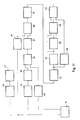
- the electronics (FIG. 11) initially have an oscillator 41 and a sine converter 42 associated therewith, with which the oscillator signal is converted into a sine wave.
- the components mentioned can be implemented using a NE 5521 module from Valvo or a corresponding module.
- an LC oscillator in particular according to Franklin, can be provided as the oscillator, which is modified such that the primary coil of the sensor 11 is connected in parallel with the capacitor of the LC oscillator and forms the inductance of the oscillator.
- a high frequency is used, which means frequencies in the range from 5 to 100 kHz. In the specific exemplary embodiment, a frequency of 58.8 KHz was used.
- the amplitude level depends on the operating voltage used and is, for example, approximately 6 V S at an operating voltage of + 10 volts.
- An increase in sensitivity can be achieved by operating the coils 13, 14, 16 in resonance by connecting suitable capacitors in parallel.
- the secondary voltages (measurement and reference voltage) induced in the secondary coils 14, 16 (FIGS. 2, 7, 8) of the sensor 11 are fed separately to an adder 45 via separate amplifiers 43, 44, one of the voltages via a phase shifter 46, if appropriate in the form of an all-pass, to zero the difference between the two voltages in the absence of the stripe pattern in question.
- the amplitude of the amplitude values is initially compared by changing gain factors in the different branches. Additionally or alternatively, the number of turns can be selected in a suitable manner. In the case of a symmetrical H-core, the turns of the secondary coils 14, 16 will be substantially the same, while in the case of an asymmetrical configuration (FIG. 3) the number of turns for zero adjustment will be chosen differently.
- phase correction must be carried out by the phase shifter 44.
- a zero adjustment could also be carried out instead of by means of a reference signal by means of a signal which simulates it completely electronically, or by compensating the measuring signal of the measuring coil 14 purely electronically or on the basis of the signal applied to the primary coil 13. In this case, the reference coil 16 could be omitted.
- the output signal of the adder 45 is then fed to a bandpass filter 47 for filtering out disturbing DC and harmonic components.
- the inductance of the exciters first coil are chosen so that the constant voltage source 41.42 supplying the sinusoidal voltage is not overloaded, which can be achieved by 150 to 200 turns of a copper enamelled wire with a diameter of 0.05 mm. If the load is not so great, the excitation resonant circuit and thus the capacitance connected in parallel with the excitation coil 13 can be dispensed with. As a result, a low-drift, stable input signal is achieved.
- the two coils can be connected in series to make a difference, i.e. against each other.
- a common capacitance for generating an oscillating circuit is connected in parallel to both.
- the detection circuit ie when the magnetic circuit is disturbed by code strips, operates the secondary circuit with the measuring and resonance coil 14, 16 into the resonance, which results in the drift behavior compared to the above-mentioned circuit, when detection occurs in the differential voltage is generated in a circle from the resonance, is reduced.
- the adjusted signal is fed - if necessary after further amplification - to a synchronous demodulator 48 (multiplier) for rectifying the secondary differential voltage by means of the primary signal.
- a synchronous demodulator 48 multiplier
- the measuring circuit 14 of the sensor 11 experiences, there is a different phase relationship between the primary and differential voltage. Since the prerequisite for synchronous rectification is phase equality or phase difference of 180 degrees between primary and differential voltage, a further phase correction between primary and differential voltage must be carried out, for which purpose a phase shifter 49 is provided in the circuit of the primary signal supplied by sine converter 42 in the embodiment shown.
- the phase shifter is preferably formed by an all-pass.
- the carrier frequency is finally filtered out by means of a low-pass filter 51.
- a low-pass filter 51 This is followed by an inverting, preferably voltage-dependent, amplifier 52.
- the further processing of the output signal of the amplifier 52 takes place via a differentiator 53, a voltage-dependent phase shifter 54 and, in a first embodiment, a comparator 56, which is not shifted and which is compared with the signal shifted by the phase shifter 54, and which is followed by an AND gate 57 which does this Comparator signal depending on the switching state of a gate circuit 58 switched by the undifferentiated signal (output of 52).
- the outlet signal of the AND gate is the desired TTL signal corresponding to strip 3, 4, which can be passed on for further evaluation and detection of the signal sequence, for example to a computer.
- FIG. 12a schematically shows an arrangement of the electrically conductive strips of a strip code, the hatched bars corresponding to the copper tracks.
- this code results in a high-frequency or carrier voltage which corresponds to the code strip and is modulated by the influence of its conductivity, which is rectified by the synchronous demodulator 48 and whose high-frequency component is filtered out by the low-pass filter, so that behind the low-pass filter 51 results in the (low frequency) signal shown in FIG. 12b.
- the narrower copper tracks achieve a significantly weaker eddy current spread compared to the wider ones and can therefore only be seen in the signal according to FIG. 12b as small, narrow positive peaks.
- a voltage-dependent amplification takes place via the inverting amplifier 52 in such a way that the narrow peaks of lower height are amplified more, i.e. are raised more than the broad ones Peaks without the latter (after inversion) going into the negative limit.
- the addition of an additional offset voltage supports the desired effect in that a very high amplification takes place in the positive range, while in the negative range it decreases logarithmically to almost 1 up to the maximum output voltage (from minus 3.3 volts).
- the voltage-dependent inverting amplifier 52 thus delivers the signal of FIG. 12c.
- FIG. OP denotes an operational amplifier, for example one with the designation TL 084, D1 is a silicon diode (for example 1 N 41 48) and D2 is a tens diode (for example ZPD 3.3).
- the input 60 coming from the synchronous modulator or the downstream low-pass filter 49 is open the negative input of the operational amplifier, while the positive input is at a fixed value (inversion).
- the voltage-dependent amplification takes place via D1, D2, while the offset voltage can be adjusted by means of the potentiometer P arranged on the left.
- the signal differentiated by the differentiator 53 is shown as signal 61 in FIG. 12d.
- the output signal of the voltage-dependent phase shifter is shown as phase-shifted signal 62.
- FIG. 14 A preferred construction of a voltage-dependent phase shifter in the circuit of FIG. 11 can be seen in FIG. 14, in which, in addition to the phase shifter 54, the downstream comparator 56 is shown.
- the phase shifter 54 consists of two antiparallel diodes D3, D4, which are connected to a capacitor C to form an RC combination.
- the voltage amount of the input signal is greater than a predetermined value (for example 0.7 volts), one of the two diodes is conductive. There is a low forward resistance. The RC combination formed results in a slight phase shift with respect to the input signal 61 (FIG. 12c). If, on the other hand, the voltage amount of the input signal is less than the aforementioned voltage value, both diodes block. There is a high blocking resistance, so that the RC combination causes a large phase shift to the input signal 61. As a result, the differentiated signals are also sufficiently far apart in the saddle area, where they run almost parallel, so that they do not cross and the comparator 56 does not perform any switching operations in this area, while the phase shift is small in the peak areas of the differentiated signal. The shifted and the undisplaced signal cross near their maxima. The comparator switches at this crossing point. Due to the small shift generated in this area, the switching point of the Kompa rators 56 a flank in the output stripe pattern very accurately again.
- a predetermined value
- the voltage-dependent phase shifter 54 can be changed by the selection and number of the anti-parallel diodes with regard to the voltage range at which a change in the phase shift occurs, while the phase shift can be varied in both areas by connecting resistors to the diodes in series.
- the comparator signal is shown in Fig.12e.
- the gate circuit 58 shown in FIG. 11 can be provided, by means of which the voltage-dependent amplified and inverted analog signal according to FIG. 12c is compared with a fixed, predeterminable threshold 64, the comparator only opening if the (inverted) analog value is below the threshold , while it closes when an inverted and offset "zero value" of the signal, as explained above, lies above the threshold, so that it does not emit an output signal and therefore the AND gate does not close any measurement in this case.
- the TTL output signal emitted by the AND gate 57 is shown in FIG. 12g. As mentioned, this can be processed further, for example in a computer.
- An alternative circuit to prevent the clocking of the comparator provides that an adder is arranged instead of the gate circuit between the voltage-dependent phase shifter and the comparator, which superimposes a negative offset voltage on the voltage-dependent phase-shifted differential signal 62, so that the "zero values" of the undisplaced and the phase-shifted signal in their values (in terms of intensity) "pulled apart".
- the voltage-dependent phase shifter is terminated by an impedance converter, the output of which supplies the input signal of the adder (not shown in detail).
- the TTL output signal of the comparator 56 can then be used directly for further processing.
- the further processing of the signal of FIG. 12c after an amplifier 52 can in principle also be carried out by peak value detection, as is explained in DE-OS 37 23 348 for an optical barcode reading system, to which express reference is made.
- the resulting desired TTL signal corresponding to strips 3, 4 is passed on for further evaluation and recognition of the signal sequence, for example to a computer.
- the logic circuit 38 of DE-OS 37 23 348 was provided to suppress the influence of the individual matrix printer dots read there and the problems associated therewith do not occur here, so that this element is not required.
- the synchronous demodulator 48 and the low-pass filter 51 of FIG. 11 can be seen in FIG. 15 by a square-wave converter 71, a subsequent retriggerable monoflop 72 in the excitation circuit and a sample-and-hold circuit 73 which is clocked by the clock of the monoflop 72 will be replaced.
- the output signal of the sample and hold circuit 73 corresponds to that of FIG. 12d.
- Another alternative is to maintain the synchronous demodulation of FIG. 11, but to replace the low-pass filter by the fact that the excitation signal is corrected relative to the measurement or difference signal via a further phase shifter 81, a square-wave converter 82 in the excitation circuit and this one subsequently Circuit for frequency doubling with oppositely arranged monoflops 83, 84 and a subsequent OR gate 85 for generating the clock for a sample-and-hold circuit 86 in the measurement signal circuit (FIG. 16).
- the individual sensors are queried successively for their respective status by means of a multiplex circuit (FIG. 17).
- the sine converter 42 is followed by a demultiplexer 91 in the excitation circuit, which sequentially assigns the excitation signal to the individual sensor cores 92, while in a corresponding sequence the measuring and possibly reference coils 14, 16 of the individual sensors 92 are queried by the multiplexer 93.
- the sequence control is carried out by a microprocessor 94.
- the further processing of the signals takes place via the amplifier 47, the synchronous demodulator 48 and the low-pass filter 51 or one of the corresponding equivalent circuits of these elements explained above.
- the differentiated voltage is represented in the manner described above (circuit blocks 66.95).
- the corresponding digital states of the individual sensors are stored in a memory 96 (RAM). From here they can be processed further via a parallel or serial interface 97,98.
- the excitation winding is, as mentioned, on the middle leg.
- the secondary windings on the two outer legs must be treated symmetrically, so that their circuit parts 66.95 are arranged in parallel on corresponding surfaces 66a, 95a. It is essential that the positioning accuracy is maintained relative to the bar code, that is, one of the two outer legs together with the middle leg above the strip, but the other is arranged outside the same.
Landscapes
- Engineering & Computer Science (AREA)
- Physics & Mathematics (AREA)
- General Physics & Mathematics (AREA)
- Theoretical Computer Science (AREA)
- Artificial Intelligence (AREA)
- Computer Vision & Pattern Recognition (AREA)
- Investigating Or Analyzing Materials By The Use Of Magnetic Means (AREA)
- Control Of Vending Devices And Auxiliary Devices For Vending Devices (AREA)
- Credit Cards Or The Like (AREA)
- Input From Keyboards Or The Like (AREA)
- Geophysics And Detection Of Objects (AREA)
- Forklifts And Lifting Vehicles (AREA)
- Pinball Game Machines (AREA)
Applications Claiming Priority (2)
| Application Number | Priority Date | Filing Date | Title |
|---|---|---|---|
| DE3931828A DE3931828A1 (de) | 1989-09-23 | 1989-09-23 | Streifencode sowie verfahren und vorrichtung zum lesen eines solchen |
| DE3931828 | 1989-09-23 |
Publications (3)
| Publication Number | Publication Date |
|---|---|
| EP0420030A2 true EP0420030A2 (fr) | 1991-04-03 |
| EP0420030A3 EP0420030A3 (en) | 1991-05-02 |
| EP0420030B1 EP0420030B1 (fr) | 1997-07-30 |
Family
ID=6390060
Family Applications (1)
| Application Number | Title | Priority Date | Filing Date |
|---|---|---|---|
| EP90118067A Expired - Lifetime EP0420030B1 (fr) | 1989-09-23 | 1990-09-20 | Code à barres ainsi que procédé et dispositif de lecture d'un tel code |
Country Status (5)
| Country | Link |
|---|---|
| US (1) | US5430278A (fr) |
| EP (1) | EP0420030B1 (fr) |
| JP (1) | JPH03208189A (fr) |
| AT (1) | ATE156283T1 (fr) |
| DE (2) | DE3931828A1 (fr) |
Cited By (6)
| Publication number | Priority date | Publication date | Assignee | Title |
|---|---|---|---|---|
| US5293031A (en) * | 1991-03-18 | 1994-03-08 | Atsutoshi Goto | Magnetic bar code reading system employing phase-shift type sensor having plural sensing sections |
| EP0565988A3 (fr) * | 1992-04-11 | 1994-04-13 | Basf Ag | |
| GB2312595A (en) * | 1996-04-23 | 1997-10-29 | Flying Null Ltd | Magnetically coded tag or marker |
| US5708545A (en) * | 1992-07-23 | 1998-01-13 | Deutsche Thomson-Brandt Gmbh | Recording device with electrical contacts |
| WO2001056787A1 (fr) * | 2000-02-02 | 2001-08-09 | Friedrich Von Rohrscheidt | Pelliculeuse a cartouche |
| GB2417857A (en) * | 2004-07-26 | 2006-03-08 | Confirm Technologies Ltd | A Magnetic Tag and System for Reading a Magnetic Tag |
Families Citing this family (31)
| Publication number | Priority date | Publication date | Assignee | Title |
|---|---|---|---|---|
| DE4208772A1 (de) * | 1992-03-19 | 1993-09-23 | Krieg Gunther | Induktiver bar-code-traeger |
| DE4224371A1 (de) * | 1992-07-23 | 1994-01-27 | Thomson Brandt Gmbh | Strich- oder Barcode-Einheit |
| US5978701A (en) * | 1995-06-02 | 1999-11-02 | Alza Corporation | Electrotransport device with separable controller and drug unit and method of setting controller output |
| US6009400A (en) * | 1996-03-05 | 1999-12-28 | Blackman; Seymour | Method and arrangement for alerting customers from purchasing perished items using bar codes with changeable properties when subjected to factors causing perishability |
| US6086572A (en) * | 1996-05-31 | 2000-07-11 | Alza Corporation | Electrotransport device and method of setting output |
| US6064315A (en) * | 1998-12-29 | 2000-05-16 | Harmon Industries, Inc. | Zero speed transducer |
| US6202929B1 (en) * | 1999-03-10 | 2001-03-20 | Micro-Epsilon Mess Technik | Capacitive method and apparatus for accessing information encoded by a differentially conductive pattern |
| DE19955464A1 (de) * | 1999-11-08 | 2001-07-19 | Heinz Brych | Vorrichtung zur Detektion und Identifikation von Gegenständen |
| FR2806483B1 (fr) * | 2000-03-14 | 2004-01-09 | Electronique Angelidis Et Sarr | Procede de detection et d'identification d'un objet parmi une pluralite d'objets, et dispositif pour sa mise en oeuvre |
| AU2001279600A1 (en) * | 2000-08-10 | 2002-02-18 | Novo-Nordisk A/S | A support for a cartridge for transferring an electronically readable information to an electronic circuit, and use of composite material in a support |
| US6547140B2 (en) * | 2000-11-29 | 2003-04-15 | Xerox Corporation | Microwave barcode reader using dipole antenna |
| US6892949B2 (en) * | 2000-12-29 | 2005-05-17 | Siemens Logistics And Assembly Systems Inc. | Low visual impact labeling method and system |
| CN1233543C (zh) * | 2001-05-31 | 2005-12-28 | 因温特奥股份公司 | 利用代码载体测定被导轨导向的电梯轿厢位置的装置 |
| JP4582564B2 (ja) * | 2001-06-25 | 2010-11-17 | ソニーマニュファクチュアリングシステムズ株式会社 | 磁束測定装置 |
| JP4762131B2 (ja) * | 2003-03-24 | 2011-08-31 | ノボ・ノルデイスク・エー/エス | 薬用カートリッジの透明な電子マーキング |
| US7284704B2 (en) * | 2004-06-28 | 2007-10-23 | International Barcode Corporation | Combined electromagnetic and optical communication system |
| JP4629393B2 (ja) * | 2004-09-10 | 2011-02-09 | 三菱電機株式会社 | ワイヤ放電加工装置 |
| DE102005008967A1 (de) * | 2005-02-28 | 2006-08-31 | Giesecke & Devrient Gmbh | Verfahren und Vorrichtung zum Messen magnetischer Eigenschaften von Dokumenten |
| FI119084B (fi) * | 2005-04-15 | 2008-07-15 | M Real Oyj | Uudet tuotteet ja menetelmä niiden valmistamiseksi |
| DE602006019712D1 (fr) * | 2005-05-10 | 2011-03-03 | Novo Nordisk As | |
| RU2432549C2 (ru) * | 2005-09-22 | 2011-10-27 | Ново Нордиск А/С | Способ и прибор для бесконтактного определения абсолютного положения и устройство, снабженное данным прибором |
| CN101405749B (zh) * | 2006-03-20 | 2012-05-30 | 诺沃—诺迪斯克有限公司 | 套筒及在套筒插入到其中时的药物输送装置 |
| EP2011223B1 (fr) | 2006-04-12 | 2018-06-13 | Novo Nordisk A/S | Détermination de la position absolue d'un membre monté de manière mobile dans un dispositif pour administrer un médicament |
| BRPI0710915A2 (pt) | 2006-04-26 | 2011-09-27 | Novo Nordisk As | dispositivo de distribuição de medicação e método para determinar posições absolutas de um primeiro membro em relação a um segundo membro de um dispositivo de distribuição de medicação |
| US8348904B2 (en) * | 2007-03-21 | 2013-01-08 | Novo Nordisk A/S | Medical delivery system having container recognition and container for use with the medical delivery system |
| CN101681421A (zh) * | 2007-06-09 | 2010-03-24 | 诺沃-诺迪斯克有限公司 | 贮存器识别码的无接触读取 |
| EP2192529A4 (fr) * | 2007-09-14 | 2011-05-04 | Tokyo Mechatronics Co Ltd | Corps de données capacitives et lecteur de données pour lecture de données capacitives |
| JP5562969B2 (ja) | 2008-11-06 | 2014-07-30 | ノボ・ノルデイスク・エー/エス | 電子的に支援された薬剤送達装置 |
| EP2396059B1 (fr) | 2009-02-13 | 2014-01-08 | Novo Nordisk A/S | Dispositif médical et cartouche |
| JP5658592B2 (ja) * | 2011-02-21 | 2015-01-28 | 国立大学法人埼玉大学 | 移動体用非接触給電装置 |
| CN102830740B (zh) * | 2012-08-23 | 2014-04-30 | 矽力杰半导体技术(杭州)有限公司 | 一种高效率的偏置电压产生电路 |
Family Cites Families (15)
| Publication number | Priority date | Publication date | Assignee | Title |
|---|---|---|---|---|
| US3188616A (en) * | 1961-08-17 | 1965-06-08 | Sperry Rand Corp | Transistor compensating circuit for magnetic recording head |
| US3358124A (en) * | 1963-07-26 | 1967-12-12 | Datamatics International Inc | Data card translating device |
| US3860796A (en) * | 1969-09-05 | 1975-01-14 | Synergistics Inc | Magnetically sensible record and process of producing same |
| US3613101A (en) * | 1970-01-21 | 1971-10-12 | Digitronics Corp | Magnetic recording utilizing a selective magnetic shielding structure |
| US3710362A (en) * | 1971-09-13 | 1973-01-09 | A Kronfeld | Hand held transducer insensitive to angular orientation |
| CH611440A5 (fr) * | 1975-12-29 | 1979-05-31 | Juergen Machate | |
| CH601863A5 (fr) * | 1976-04-28 | 1978-07-14 | Sodeco Compteurs De Geneve | |
| US4130242A (en) * | 1977-09-08 | 1978-12-19 | Continental Instrument Corporation | Data storage and retrieval system employing balanced magnetic circuits |
| DE2832719A1 (de) * | 1978-07-26 | 1980-02-07 | Basf Ag | Anordnung zur kompensation von ungleichen schreibfeldern in magnetischen datenspeichereinrichtungen, insbesondere in magnetplattenspeichern |
| US4218612A (en) * | 1978-10-05 | 1980-08-19 | Docutronix, Inc. | Magnetic signal detector |
| US4314289A (en) * | 1979-12-07 | 1982-02-02 | International Business Machines Corporation | Biased pulsed recording systems and methods |
| US4281242A (en) * | 1980-02-11 | 1981-07-28 | Continental Instruments Corporation | Balancing apparatus for magnetic circuits employed in data storage and retrieval systems |
| DE3521095C2 (de) * | 1985-06-12 | 1987-04-09 | Nixdorf Computer Ag, 4790 Paderborn | Einrichtung zum Erkennen und Prüfen von Magnetschichtmedien |
| FR2617628A1 (fr) * | 1987-02-23 | 1989-01-06 | Lehry Jean | Carte a induction et lecteur associe |
| JPH0739063Y2 (ja) * | 1987-03-13 | 1995-09-06 | グローリー工業株式会社 | 磁気及び光センサ |
-
1989
- 1989-09-23 DE DE3931828A patent/DE3931828A1/de not_active Withdrawn
-
1990
- 1990-09-20 EP EP90118067A patent/EP0420030B1/fr not_active Expired - Lifetime
- 1990-09-20 AT AT90118067T patent/ATE156283T1/de active
- 1990-09-20 DE DE59010741T patent/DE59010741D1/de not_active Expired - Fee Related
- 1990-09-25 JP JP2252041A patent/JPH03208189A/ja active Pending
-
1992
- 1992-11-16 US US07/977,254 patent/US5430278A/en not_active Expired - Fee Related
Cited By (7)
| Publication number | Priority date | Publication date | Assignee | Title |
|---|---|---|---|---|
| US5293031A (en) * | 1991-03-18 | 1994-03-08 | Atsutoshi Goto | Magnetic bar code reading system employing phase-shift type sensor having plural sensing sections |
| EP0565988A3 (fr) * | 1992-04-11 | 1994-04-13 | Basf Ag | |
| US5708545A (en) * | 1992-07-23 | 1998-01-13 | Deutsche Thomson-Brandt Gmbh | Recording device with electrical contacts |
| GB2312595A (en) * | 1996-04-23 | 1997-10-29 | Flying Null Ltd | Magnetically coded tag or marker |
| GB2312595B (en) * | 1996-04-23 | 1999-02-24 | Flying Null Ltd | Improved methods for coding magnetic tags |
| WO2001056787A1 (fr) * | 2000-02-02 | 2001-08-09 | Friedrich Von Rohrscheidt | Pelliculeuse a cartouche |
| GB2417857A (en) * | 2004-07-26 | 2006-03-08 | Confirm Technologies Ltd | A Magnetic Tag and System for Reading a Magnetic Tag |
Also Published As
| Publication number | Publication date |
|---|---|
| DE3931828A1 (de) | 1991-04-04 |
| JPH03208189A (ja) | 1991-09-11 |
| DE59010741D1 (de) | 1997-09-04 |
| US5430278A (en) | 1995-07-04 |
| EP0420030A3 (en) | 1991-05-02 |
| EP0420030B1 (fr) | 1997-07-30 |
| ATE156283T1 (de) | 1997-08-15 |
Similar Documents
| Publication | Publication Date | Title |
|---|---|---|
| EP0420030B1 (fr) | Code à barres ainsi que procédé et dispositif de lecture d'un tel code | |
| EP0170723B1 (fr) | Procédé et dispositif pour augmenter la sensibilité des capteurs de déplacement à distance | |
| DE60130700T2 (de) | Induktiver Positionsgeber | |
| DE3913861A1 (de) | Verlagerungs-detektor | |
| DE10350733A1 (de) | Induktiver Näherungsschalter mit Differenzspulenanordnung | |
| EP0473808A1 (fr) | Dispositif de mesure pour la détermination d'un trajet ou d'une position | |
| DE102004033083A1 (de) | Wirbelstromsensor zur kontinuierlichen Weg- oder Winkelmessung | |
| DE2916289C2 (de) | Messung der Magnetflußänderung und der LuftspaltgröBe eines Luftspaltes zwischen einem Elektromagneten und einem ferromagnetischen Material | |
| WO2010069285A2 (fr) | Ensemble capteur et procédé pour déterminer la position et/ou le changement de position d'un objet de mesure | |
| EP3824323B1 (fr) | Détecteur servant à détecter du matériau électriquement conducteur | |
| DE2636586B2 (de) | Einrichtung zur Messung einer im wesentlichen linearen Verschiebung eines Körpers mit einer festen Spule | |
| DE4425903A1 (de) | Vorrichtung mit einem Meßtransformator zur Erfassung der Position eines linear beweglichen Objektes | |
| WO2013149949A1 (fr) | Procédé et ensemble et capteur permettant de déterminer la position d'un élément | |
| DE3100486A1 (de) | Vorrichtung zur bestimmung der position eines schweissgeraetes zum selbsttaetigen lichtbogenschweissen | |
| EP0945381A2 (fr) | Appareil de mesure de la position d'une tÔle métallique au moyen inductif | |
| DE3715789C2 (fr) | ||
| AT510240A2 (de) | Positionsmesseinrichtung mit randkompensation | |
| DE102007011952B4 (de) | Bewegungsmessvorrichtung, insbesondere Drehwinkelgeber | |
| DE10248954A1 (de) | Sicherheitselement für Ausweis- und Wertdokumente | |
| DE2722544C2 (de) | Meßvorrichtung zur induktiven Umformung von Lageänderungen eines Gegenstandes | |
| DE20120658U1 (de) | Induktive Positionserkennungsvorrichtung | |
| DE102023201023A1 (de) | Induktive Positionsmesseinrichtung | |
| EP2428773B1 (fr) | Capteur de trajectoire analogique à phases | |
| DE102023102164B4 (de) | Sekundärspulenanordnung für einen induktiven Encoder | |
| DE3409448C2 (fr) |
Legal Events
| Date | Code | Title | Description |
|---|---|---|---|
| PUAI | Public reference made under article 153(3) epc to a published international application that has entered the european phase |
Free format text: ORIGINAL CODE: 0009012 |
|
| PUAL | Search report despatched |
Free format text: ORIGINAL CODE: 0009013 |
|
| AK | Designated contracting states |
Kind code of ref document: A2 Designated state(s): AT BE CH DE DK ES FR GB IT LI NL SE |
|
| AK | Designated contracting states |
Kind code of ref document: A3 Designated state(s): AT BE CH DE DK ES FR GB IT LI NL SE |
|
| 17P | Request for examination filed |
Effective date: 19911102 |
|
| 17Q | First examination report despatched |
Effective date: 19941130 |
|
| GRAG | Despatch of communication of intention to grant |
Free format text: ORIGINAL CODE: EPIDOS AGRA |
|
| GRAH | Despatch of communication of intention to grant a patent |
Free format text: ORIGINAL CODE: EPIDOS IGRA |
|
| GRAH | Despatch of communication of intention to grant a patent |
Free format text: ORIGINAL CODE: EPIDOS IGRA |
|
| GRAA | (expected) grant |
Free format text: ORIGINAL CODE: 0009210 |
|
| AK | Designated contracting states |
Kind code of ref document: B1 Designated state(s): AT BE CH DE DK ES FR GB IT LI NL SE |
|
| PG25 | Lapsed in a contracting state [announced via postgrant information from national office to epo] |
Ref country code: IT Free format text: LAPSE BECAUSE OF FAILURE TO SUBMIT A TRANSLATION OF THE DESCRIPTION OR TO PAY THE FEE WITHIN THE PRE;WARNING: LAPSES OF ITALIAN PATENTS WITH EFFECTIVE DATE BEFORE 2007 MAY HAVE OCCURRED AT ANY TIME BEFORE 2007. THE CORRECT EFFECTIVE DATE MAY BE DIFFERENT FROM THE ONE RECORDED.SCRIBED TIME-LIMIT Effective date: 19970730 Ref country code: ES Free format text: THE PATENT HAS BEEN ANNULLED BY A DECISION OF A NATIONAL AUTHORITY Effective date: 19970730 Ref country code: DK Effective date: 19970730 Ref country code: NL Free format text: LAPSE BECAUSE OF FAILURE TO SUBMIT A TRANSLATION OF THE DESCRIPTION OR TO PAY THE FEE WITHIN THE PRESCRIBED TIME-LIMIT Effective date: 19970730 Ref country code: GB Free format text: LAPSE BECAUSE OF FAILURE TO SUBMIT A TRANSLATION OF THE DESCRIPTION OR TO PAY THE FEE WITHIN THE PRESCRIBED TIME-LIMIT Effective date: 19970730 Ref country code: FR Effective date: 19970730 |
|
| REF | Corresponds to: |
Ref document number: 156283 Country of ref document: AT Date of ref document: 19970815 Kind code of ref document: T |
|
| REG | Reference to a national code |
Ref country code: CH Ref legal event code: EP |
|
| REF | Corresponds to: |
Ref document number: 59010741 Country of ref document: DE Date of ref document: 19970904 |
|
| PG25 | Lapsed in a contracting state [announced via postgrant information from national office to epo] |
Ref country code: BE Free format text: LAPSE BECAUSE OF NON-PAYMENT OF DUE FEES Effective date: 19970930 |
|
| PG25 | Lapsed in a contracting state [announced via postgrant information from national office to epo] |
Ref country code: SE Effective date: 19971030 |
|
| PGFP | Annual fee paid to national office [announced via postgrant information from national office to epo] |
Ref country code: AT Payment date: 19971114 Year of fee payment: 8 |
|
| PGFP | Annual fee paid to national office [announced via postgrant information from national office to epo] |
Ref country code: DE Payment date: 19971127 Year of fee payment: 8 |
|
| EN | Fr: translation not filed | ||
| PGFP | Annual fee paid to national office [announced via postgrant information from national office to epo] |
Ref country code: CH Payment date: 19971229 Year of fee payment: 8 |
|
| NLV1 | Nl: lapsed or annulled due to failure to fulfill the requirements of art. 29p and 29m of the patents act | ||
| GBV | Gb: ep patent (uk) treated as always having been void in accordance with gb section 77(7)/1977 [no translation filed] |
Effective date: 19970730 |
|
| REG | Reference to a national code |
Ref country code: CH Ref legal event code: NV Representative=s name: TROESCH SCHEIDEGGER WERNER AG |
|
| BERE | Be: lapsed |
Owner name: KRIEG GUNTHER Effective date: 19970930 |
|
| PLBE | No opposition filed within time limit |
Free format text: ORIGINAL CODE: 0009261 |
|
| STAA | Information on the status of an ep patent application or granted ep patent |
Free format text: STATUS: NO OPPOSITION FILED WITHIN TIME LIMIT |
|
| 26N | No opposition filed | ||
| PG25 | Lapsed in a contracting state [announced via postgrant information from national office to epo] |
Ref country code: AT Free format text: LAPSE BECAUSE OF NON-PAYMENT OF DUE FEES Effective date: 19980920 |
|
| PG25 | Lapsed in a contracting state [announced via postgrant information from national office to epo] |
Ref country code: LI Free format text: LAPSE BECAUSE OF NON-PAYMENT OF DUE FEES Effective date: 19980930 Ref country code: CH Free format text: LAPSE BECAUSE OF NON-PAYMENT OF DUE FEES Effective date: 19980930 |
|
| REG | Reference to a national code |
Ref country code: CH Ref legal event code: PL |
|
| PG25 | Lapsed in a contracting state [announced via postgrant information from national office to epo] |
Ref country code: DE Free format text: LAPSE BECAUSE OF NON-PAYMENT OF DUE FEES Effective date: 19990701 |