EP0420161A2 - Condensateur électrique - Google Patents
Condensateur électrique Download PDFInfo
- Publication number
- EP0420161A2 EP0420161A2 EP90118413A EP90118413A EP0420161A2 EP 0420161 A2 EP0420161 A2 EP 0420161A2 EP 90118413 A EP90118413 A EP 90118413A EP 90118413 A EP90118413 A EP 90118413A EP 0420161 A2 EP0420161 A2 EP 0420161A2
- Authority
- EP
- European Patent Office
- Prior art keywords
- tear
- wire
- capacitor
- soldered
- point
- Prior art date
- Legal status (The legal status is an assumption and is not a legal conclusion. Google has not performed a legal analysis and makes no representation as to the accuracy of the status listed.)
- Withdrawn
Links
Images
Classifications
-
- H—ELECTRICITY
- H01—ELECTRIC ELEMENTS
- H01G—CAPACITORS; CAPACITORS, RECTIFIERS, DETECTORS, SWITCHING DEVICES, LIGHT-SENSITIVE OR TEMPERATURE-SENSITIVE DEVICES OF THE ELECTROLYTIC TYPE
- H01G2/00—Details of capacitors not covered by a single one of groups H01G4/00-H01G11/00
- H01G2/14—Protection against electric or thermal overload
Definitions
- the invention relates to an electrical capacitor, in particular a power capacitor, which is installed in a housing in which an overpressure tear-off safety device is arranged, which consists of a wire with a predetermined tear-off point, which is passed through the housing cover in an insulated manner and is soldered.
- Tear-off devices respond to overpressure in a capacitor. This is done by tearing off the electrical lines at a defined break point.
- the line is usually attached between a "fixed” clamping point (e.g. on the Schoop layer of the capacitor winding) and a part that moves when pressure builds up (usually the top or bottom of the capacitor housing).
- the line When fastening in the cover, the line is insulated through the cover (metallized ceramic) and soldered in a solderable metal part.
- the object of the invention is the condensates mentioned sator to develop such that the difficulties outlined above can be prevented in a simple manner.
- This object is achieved in that a clamping part is arranged on the tear-off wire.
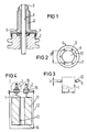
- FIG. 1 shows a tear-off wire 1 which is provided with a nominal tear-off point (not shown in the FIG.) And one end of which is fixed, for example, to the Schoop layer of the capacitor winding.
- An insulated ceramic bushing 2 is arranged in the cover of the capacitor housing, to which a metallic connection element 3 is contacted by the solder 4. Connection 3 and bushing 2 have bores through which the tear-off wire 1 is guided and is fixed to the solder 5 at the upper end of the metallic connection 3. Before the solder connections 4, 5 are attached, a clamping part 6 is pushed over the wire 1 from above.
- FIG. 2 shows a plan view of the clamping part 6, which consists of a metallic disc 7, into which a hole 8 with the diameter d 1 and slots 9 are punched.
- the diameter d 1 of the hole 8 is chosen such that it is smaller than the diameter d of the tear-off wire, so that the sections 10, which are arranged between the slots 7, "slide up" the tear-off wire when pushed on, and thus fix the tear-off wire.
- FIG 3 shows a section through the clamping part 6, the the tear-off wire 1 with the diameter d is pushed on.
- the sections 10 are bent upwards by the amount H, so that the tear-off wire 1 is clamped.
- a passage of liquid solder when the soldering point overheats is prevented by the sections 10 which abut the tear-off wire 1.
- a subsequent squeezing of the tear-off wire 1 is also not necessary, so that damage to the target tear-off point is avoided.
- FIG. 4 shows an embodiment in which a capacitor winding 11 is installed in a housing 12.
- the tear-off wire 1 has a predetermined tear-off point 13 and is fastened to the lower end contact layer 14 of the capacitor winding 11, e.g. welded on.
- Ceramic bushings 2 are arranged in the cover of the housing 15, onto which metal connection elements 3 are soldered.
- the connection elements 3 are connected to the electrical supply lines 16 of the capacitor, in which one is formed by the tear-off wire 1.
Landscapes
- Engineering & Computer Science (AREA)
- Power Engineering (AREA)
- Microelectronics & Electronic Packaging (AREA)
- Fixed Capacitors And Capacitor Manufacturing Machines (AREA)
Applications Claiming Priority (2)
| Application Number | Priority Date | Filing Date | Title |
|---|---|---|---|
| DE3932252 | 1989-09-27 | ||
| DE3932252 | 1989-09-27 |
Publications (2)
| Publication Number | Publication Date |
|---|---|
| EP0420161A2 true EP0420161A2 (fr) | 1991-04-03 |
| EP0420161A3 EP0420161A3 (en) | 1991-09-18 |
Family
ID=6390305
Family Applications (1)
| Application Number | Title | Priority Date | Filing Date |
|---|---|---|---|
| EP19900118413 Withdrawn EP0420161A3 (en) | 1989-09-27 | 1990-09-25 | Electric capacitor |
Country Status (1)
| Country | Link |
|---|---|
| EP (1) | EP0420161A3 (fr) |
Cited By (1)
| Publication number | Priority date | Publication date | Assignee | Title |
|---|---|---|---|---|
| EP0693758A1 (fr) * | 1994-07-20 | 1996-01-24 | ALPES TECHNOLOGIES (société anonyme) | Condensateur avec protection contre la surpression |
Family Cites Families (3)
| Publication number | Priority date | Publication date | Assignee | Title |
|---|---|---|---|---|
| DE2418579B2 (de) * | 1974-04-17 | 1976-08-19 | Standard Elektrik Lorenz Ag, 7000 Stuttgart | Elektrischer wickelkondensator |
| DE3320703A1 (de) * | 1983-06-08 | 1984-12-13 | Siemens AG, 1000 Berlin und 8000 München | Schraubanschluss fuer elektrische kondensatoren |
| EP0284927B1 (fr) * | 1987-03-19 | 1992-07-15 | Siemens Aktiengesellschaft | Condensateur électrique |
-
1990
- 1990-09-25 EP EP19900118413 patent/EP0420161A3/de not_active Withdrawn
Cited By (2)
| Publication number | Priority date | Publication date | Assignee | Title |
|---|---|---|---|---|
| EP0693758A1 (fr) * | 1994-07-20 | 1996-01-24 | ALPES TECHNOLOGIES (société anonyme) | Condensateur avec protection contre la surpression |
| FR2722911A1 (fr) * | 1994-07-20 | 1996-01-26 | Alpes Technologies | Condensateur autoprotege par sectionnement |
Also Published As
| Publication number | Publication date |
|---|---|
| EP0420161A3 (en) | 1991-09-18 |
Similar Documents
| Publication | Publication Date | Title |
|---|---|---|
| EP0374648B1 (fr) | Dispositif de connexion d'un câble électrique | |
| DE2107218C3 (de) | Verwendung einer Kastenklemme und Kastenklemme hierfür | |
| DE69834160T2 (de) | Verbindungsverfahren und Verbindungsstruktur eines elektronischen Bauteils an einem elektromagnetischen Relais | |
| DE3626151A1 (de) | Spannungszufuehrung fuer eine integrierte halbleiterschaltung | |
| EP0420161A2 (fr) | Condensateur électrique | |
| WO1997017711A2 (fr) | Dispositif de connexion | |
| DE102004049575A1 (de) | Elektrisches Anschlusselement und Verfahren zum Anschließen eines Leiterkabels | |
| DE10124117C2 (de) | Leiterplatine mit kontaktiertem SMD-Baustein sowie zugehöriger SMD-Baustein | |
| DE3028570A1 (de) | Verfahren zum kontaktieren von halbleiterbauelementen | |
| EP0418555B1 (fr) | Procédé de fabrication d'un condensateur à électrolyte solide sous forme de chip | |
| DE2117844A1 (de) | Kontaktierungsanordnung fur inte gnerte Schaltkreisbausteine (IC Bau steine) | |
| DE20019171U1 (de) | Crimpkontakt für Leiterplatten | |
| DE3936110C2 (de) | Lötstift mit Anwickelscheren für Hochtemperaturlackdrähte | |
| DE2301676C3 (de) | Unterbrecherkontakt | |
| EP0075220B1 (fr) | Filtre anti-parasitage | |
| EP0418562A2 (fr) | Procédé de fabrication d'un condensateur à électrolyte solide sous forme de chip avec élément de sécurité | |
| DE19528315C2 (de) | Verfahren zum Löten eines isolierten Drahtes | |
| DE20104407U1 (de) | Leitungsverbinder | |
| DE3927690C2 (de) | Oberflächenmontierbarer Widerstand | |
| DE102017117179A1 (de) | Geräteanordnung | |
| EP0709864B1 (fr) | Transformateur encapsulé en résine coulée | |
| DE19654384A1 (de) | Anschlußklemmen für elektrische Geräte | |
| AT230460B (de) | Anordnung von Bauelementen, insbesondere von Baugruppen in gedruckten Schaltungen od. dgl. | |
| EP0529146A1 (fr) | Enroulement pour la commande électromagnétique d'un appareil interrupteur | |
| DE102004021654A1 (de) | Anordnung von Leiterplatten |
Legal Events
| Date | Code | Title | Description |
|---|---|---|---|
| PUAI | Public reference made under article 153(3) epc to a published international application that has entered the european phase |
Free format text: ORIGINAL CODE: 0009012 |
|
| 17P | Request for examination filed |
Effective date: 19901220 |
|
| AK | Designated contracting states |
Kind code of ref document: A2 Designated state(s): CH DE FR GB IT LI |
|
| PUAL | Search report despatched |
Free format text: ORIGINAL CODE: 0009013 |
|
| AK | Designated contracting states |
Kind code of ref document: A3 Designated state(s): CH DE FR GB IT LI |
|
| STAA | Information on the status of an ep patent application or granted ep patent |
Free format text: STATUS: THE APPLICATION IS DEEMED TO BE WITHDRAWN |
|
| 18D | Application deemed to be withdrawn |
Effective date: 19940401 |