EP0420182A2 - Nonvolatile memory cell and its manufacturing method - Google Patents
Nonvolatile memory cell and its manufacturing method Download PDFInfo
- Publication number
- EP0420182A2 EP0420182A2 EP90118464A EP90118464A EP0420182A2 EP 0420182 A2 EP0420182 A2 EP 0420182A2 EP 90118464 A EP90118464 A EP 90118464A EP 90118464 A EP90118464 A EP 90118464A EP 0420182 A2 EP0420182 A2 EP 0420182A2
- Authority
- EP
- European Patent Office
- Prior art keywords
- insulation film
- mosfet
- memory cell
- gate
- impurity region
- Prior art date
- Legal status (The legal status is an assumption and is not a legal conclusion. Google has not performed a legal analysis and makes no representation as to the accuracy of the status listed.)
- Granted
Links
Images


Classifications
-
- G—PHYSICS
- G11—INFORMATION STORAGE
- G11C—STATIC STORES
- G11C16/00—Erasable programmable read-only memories
- G11C16/02—Erasable programmable read-only memories electrically programmable
- G11C16/04—Erasable programmable read-only memories electrically programmable using variable threshold transistors, e.g. FAMOS
- G11C16/0466—Erasable programmable read-only memories electrically programmable using variable threshold transistors, e.g. FAMOS comprising cells with charge storage in an insulating layer, e.g. metal-nitride-oxide-silicon [MNOS], silicon-oxide-nitride-oxide-silicon [SONOS]
-
- G—PHYSICS
- G11—INFORMATION STORAGE
- G11C—STATIC STORES
- G11C16/00—Erasable programmable read-only memories
- G11C16/02—Erasable programmable read-only memories electrically programmable
- G11C16/06—Auxiliary circuits, e.g. for writing into memory
- G11C16/34—Determination of programming status, e.g. threshold voltage, overprogramming or underprogramming, retention
-
- H—ELECTRICITY
- H10—SEMICONDUCTOR DEVICES; ELECTRIC SOLID-STATE DEVICES NOT OTHERWISE PROVIDED FOR
- H10B—ELECTRONIC MEMORY DEVICES
- H10B69/00—Erasable-and-programmable ROM [EPROM] devices not provided for in groups H10B41/00 - H10B63/00, e.g. ultraviolet erasable-and-programmable ROM [UVEPROM] devices
-
- H—ELECTRICITY
- H10—SEMICONDUCTOR DEVICES; ELECTRIC SOLID-STATE DEVICES NOT OTHERWISE PROVIDED FOR
- H10D—INORGANIC ELECTRIC SEMICONDUCTOR DEVICES
- H10D8/00—Diodes
- H10D8/812—Charge-trapping diodes
Definitions
- the present invention relates to a nonvolatile memory cell that is capable of being electrically written, read and erased depending on carriers captured by or released from carrier traps formed in a gate insulation film of the memory cell. It also relates to a method of manufacturing the nonvolatile memory cell.
- a known nonvolatile memory device capable of being electrically written, read and erased is an EEPROM.
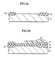
- Figures 1a and 1b show a memory cell comprising a transistor having a floating gate, of the EEPROM.
- a bias voltage of about, for example, 20 V is applied to a control gate 4 and a bias voltage of about 0 V to a drain region 2 formed on a semiconductor substrate 1, thereby injecting electrons from the drain region 2 into a floating gate 3.
- a bias voltage of about 0 V is applied to the control gate 4 and a bias voltage of about 20 V to the drain region 2, thereby releasing electrons from the floating gate 3 toward the drain region 2.
- Figure 2 shows a memory device comprising a matrixed array of memory cells each including only the above-mentioned transistor.
- a bias voltage of about 0 V is applied to a word line WL1 and a bias voltage of about 20 V to a bit line BL1, thereby establishing a write state of the cell 1.
- a cell 3 Due to the bias voltage of about 20 V on the bit line BL1, a cell 3 will be written if a bias voltage of about 0 V is applied to a word line WL2. To avoid this, a bias voltage of about 20 V is applied to the word line WL2. Also, due to the bias voltage of about 0 V on the word line WL1, a cell 2 will be written if a bias voltage of about 20 V is applied to a bit line BL2. To avoid this, a bias voltage of about 0 V is applied to the bit line BL2.
- a cell 4 With the word line WL1 being provided with 0 V, word line WL2 with 20 V, bit line BL1 with 20 V and bit line BL2 with 0 V, a cell 4 receives the bias voltage of about 0 V through its drain region and the bias voltage of about 20 V through its control gate, as shown in Fig. 1a. As a result, the cell 4 will be erased to lose information stored therein.
- each memory cell includes only the transistor of Fig. 1, the memory cells may interact with one another. It is then impossible to select only one of the memory cells to write or erase the one.
- each memory cell comprises a transistor 6 with a floating gate, and a transfer transistor 5.
- the transistors 5 and 6 are connected in series between a bit line and a ground. By controlling the transfer transistors 5, it is possible to select only one memory cell to write or erase the one.
- Fig. 3 The structure of Fig. 3, however, needs two transistors for each memory cell.
- the electrically writable and erasable nonvolatile memory cells each composed of a single transistor having a floating gate interact with one another, so that it is impossible to select and write or erase each of the cells.
- the arrangement with the transfer transistors requires two elements for each memory cell, thereby increasing an area of each cell to hinder high integration.
- the nonvolatile memory cell having the floating gate requires complicated manufacturing processes compared with a normal MOSFET, due to the floating gate. This increases manufacturing costs.
- an object of the present invention is to provide a novel nonvolatile memory cell that is capable of being electrically written, read and erased according to carriers captured by or released from carrier traps formed in a gate insulation film of the memory cell, and a method of manufacturing this sort of nonvolatile memory cell.
- Another object of the present invention is to provide an array of nonvolatile memory cells capable of being selectively written, read and erased, occupying a small area for the sake of high integration, and being simple to manufacture.
- the present invention provides a nonvolatile memory cell comprising a semiconductor substrate of first conduction type, a high-concentration impurity region of second conduction type formed on the semiconductor substrate and connected to a bit line, an insulation film in which carrier traps are formed, and a gate electrode that is opposite the high-concentration impurity region across the insulation film and connected to a word line.
- Carriers are captured by and released from the carrier traps formed in the insulation film, in response to bias voltages applied to the word and bit lines.
- Information stored in the memory cell depends on whether or not the carrier traps are holding carriers, and the information is read out of the memory cell as the difference of a tunneling current flowing between the semiconductor substrate and the high-concentration impurity region.
- an amount of the tunneling current flowing between the semiconductor substrate and the high-concentration impurity region in an area where the gate electrode faces the high-concentration impurity region is controlled according to the strength of a vertical electric field that changes depending on carriers captured by or released from the carrier traps formed in the area. Namely, an information storage function of the memory cell is realized by the tunneling current that drastically changes depending on whether or not the carrier traps are holding the carriers.
- the amount of the tunneling current controlled by the magnitude of the vertical electric field is influenced by the side of a band gap of the high-concentration impurity region that is facing the gate electrode.
- the present invention also provides a memory cell comprising a first MOSFET acting as a select transistor and a second MOSFET for storing information.
- the first and second MOSFETs are connected in series.
- an effective channel length of the second MOSFET is reduced. This increases a short channel effect, decreases a threshold voltage, and drastically changes current-voltage characteristics of the second MOSFET, thereby storing the information in the second MOSFET.
- a gate insulation film of the second MOSFET includes carrier traps, and depending on whether or not the carrier traps are holding carriers, the current-voltage characteristics of the second MOSFET change drastically.
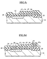
- Figure 4 is a sectional view showing a nonvolatile memory cell according to the embodiment of the present invention. This embodiment involves a PN junction formed on a semiconductor substrate, and a gate electrode formed at the PN junction to realize a nonvolatile storage function.
- a silicon semiconductor substrate 11 is of, for example, P type.
- N-type impurities such as arsenic impurities of 5x1018 cm ⁇ 3 or over are implanted to the surface of the substrate 11 to form a high-concentration impurity region (a drain region) 12.
- the drain region 12 and substrate 11 form the PN junction.
- a gate insulation film 14 such as a silicon oxide film is formed on the substrate 11.
- Carrier traps (hole traps) 13 of about 5x1012 cm ⁇ 2 are formed in the gate insulation film 14.
- a gate electrode 15 of polycrystalline silicon is formed on the gate insulation film 14. The gate electrode 15 partly faces the drain region 12 across the gate insulation film 14.
- An insulation film 16 is formed over the drain region 12 and gate electrode 15. Contact holes 17a and 17b are formed through the insulation film 16, and a drain wire 18 and a gate electrode wire 19 are connected to the drain region 12 and gate electrode 15 through the contact holes 17a and 17b, respectively.
- the above arrangement forms one memory cell which is separated from adjacent memory cells by an element separation region 20.
- a P-type silicon substrate 11 having impurities of, for example, 1x1016 cm ⁇ 3 is selectively oxidized to form an element separation region 20 around an area where a memory cell is to be formed.
- the surface of the substrate 11 is thermally oxidized at a temperature of about 900 degrees centigrade to form a gate insulation film 14, i.e., a silicon oxide film of about 250 angstroms in thickness.
- a polycrystalline silicon layer 21 is deposited to a thickness of about 3000 angstroms by, for example, a CVD method.
- the layer 21 will be a gate electrode 15.
- Phosphorus impurities are implanted and diffused to the polycrystalline silicon layer 21 to about 1x1020 cm ⁇ 3 in concentration.
- the layer 21 is then coated with resist.
- the resist is patterned to a resist pattern 22 of Fig. 5b on a part of the layer 21 where the gate electrode 15 is formed.
- the resist pattern 22 is used an a mask, and the polycrystalline silicon layer 21 is partly etched and removed by, for example, an RIE method, thereby forming the gate electrode 15.
- the material is then annealed for about 60 minutes in a nitrogen atmosphere at about 1000 degrees centigrade. This forms carrier traps (hole traps) 13 of about 5x1012 cm ⁇ 2 in the gate insulation film 14.
- Impurities such as arsenic of about 1x1015 cm ⁇ 2 are ion-implanted to the substrate 11 at energy of about 160 keV, thereby forming, in a self-aligning manner, a high-concentration impurity region (a drain region) 12 on the surface of the substrate 11.
- thermal diffusion is carried out on the material for about 30 minutes at about 900 degrees centigrade. This activates the impurities in the high-concentration impurity region 12, cures damages caused by the ion implantation, and horizontally diffuses the impurities, thereby completing the high-concentration drain region 12. A part of the drain region 12 faces the gate electrode 15 across the gate insulation film 14. An insulation film 16 is then deposited over the material by, for example, the CVD method to a thickness of about 3000 angstroms, as shown in Fig. 5c.
- Contact holes 17a and 17b are opened through the insulation film 16 to reach the gate electrode 15 and drain region 12, respectively.
- a drain wire 18 and a gate electrode wire 19 both made of, for example, aluminum are arranged through the contact holes 17a and 17b, respectively, thereby completing the memory cell shown in Fig. 5d.
- This memory cell corresponds to the one shown in Fig. 4.
- a current flowing between the substrate 11 and the drain region 12 changes depending on applied bias voltages.
- the changes in the current are related to binary information, thereby realizing a storage function of the memory cell.
- the current flowing between the substrate 11 and the drain region 12 mainly passes an area where the drain region 12 faces the gate electrode 15 with the gate insulation film 14 being between them.
- This current is a tunneling current generated by electrons that tunnel an interface between the drain region 12 and the gate insulation film 14 from a valence band to a conduction band (inter-band tunneling).
- This inter-band tunneling current occurs in an overlap area of the high-concentration drain region and gate, and is described in, for example, "IEEE Electron Device Letters" Vol. EDL-8, No. 11, November 1987, pp. 515 to 517.
- Id A x Ex x exp (-B/Es)
- Es the vertical electric field at the interface between the silicon substrate and the gate insulation film.
- the tunneling current Id drastically changes depending on changes in the vertical electric field Es.
- the carrier traps 13 formed in the gate insulation film 14 in the area where the tunneling current occurs and where the drain region 12 faces the gate electrode 15 capture carriers, which then change the vertical electric field.
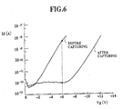
- Figure 6 is a graph showing relations of an inter-band tunneling current and a gate voltage of the memory cell formed on the P-type substrate 11, before and after the carrier traps 13 capture carriers.
- the number of the carrier traps is about 5x1012 cm ⁇ 2.
- a bias voltage of about 0 V is applied to the substrate 11 and a bias voltage of about 2 V to the drain region 12
- no carrier is captured by the carrier traps.
- a bias voltage of about -8 V is applied to the substrate 11 and a bias voltage of about -20 V to the gate electrode 15
- carriers are captured by the carrier traps 13 in the gate insulation film 14.
- Measured values of the gate voltage Vg and tunneling current Id of the carrier-not-captured state and carrier-captured state are shown in Fig. 6.
- the inter-band tunneling phenomenon produces electron-hole pairs.
- the holes run on the interface between the substrate 11 and the gate insulation film 14 and some of them surmount an energy barrier between the silicon substrate 11 and the gate insulation film (silicon oxide film) 14, because the holes receive sufficient energy from an electric field produced by the bias voltages. And the holes are captured as captured carriers by the carrier traps 13 in the film 14.
- a value of the gate voltage Vg at which the tunneling current starts to increase shifts by about 6 V before and after the carrier capturing.
- a value of the tunneling current Id with the gate voltage being about -6 V changes by about 104 times before and after the carrier capturing.
- the tunneling current drastically changes in response to the carrier capturing/releasing, i.e., the strength of the vertical electric field in the area where the tunneling current occurs.
- These changes of the current are related to binary information, thereby realizing the information storing function of the memory cell.
- a bias voltage of about -20 V is applied to the gate electrode 15 and a bias voltage of about -8 V to the substrate 11, so that the carrier traps 13 capture carriers. At this time, if the bias voltage is applied to only one of the gate electrode 15 and substrate 11, the carrier traps 13 do not capture the carriers. This means that any memory cell can uniquely be selected to write.
- the carriers captured by the carrier traps 13 are released to reestablish the carrier-not-captured state.
- a positive voltage of about 20 V, for example, is applied to the gate electrode 15.
- FIG. 7 shows another embodiment of the present invention.
- a nonvolatile memory cell comprises a high-concentration region formed in a semiconductor substrate, a PN junction formed between the high-concentration region and the substrate, and a gate electrode.
- this embodiment embeds a material to a part of the high-concentration region where the inter-band tunneling occurs to provide the part with a different band gap.
- the memory cell of Fig. 7 comprises, for example, a P-type silicon semiconductor substrate 31.
- N-type impurities such as phosphorus of 5x1018 cm ⁇ 3 or over are implanted to the surface of the substrate 31 to form a high-concentration impurity region (a drain region) 32a.
- the drain region 32a and a well region 31 form a PN junction.
- a gate insulation film 34 made of, for example, a silicon oxide film is formed on the substrate 31.
- Carrier traps 33 of about 5x1012 cm ⁇ 2 are formed in the gate insulation film 94.
- a gate electrode 35 made of, for example, aluminum is formed on the gate insulation film 34.
- the drain region 32a and gate electrode 35 partly face each other across the gate insulation film 34.
- Material such as mixed crystals of germanium and silicon that provides a different band gap is embedded to an area 36 of the drain region 32a where the inter-band tunneling occurs.
- An insulation film 37 is entirely deposited.
- Contact holes 38 reaching the drain region 32a and gate electrode 35, respectively, are formed through the insulation film 37, and a drain wire 39 and a gate electrode wire 40 are connected to the drain region 32a and gate electrode 35, respectively, through the contact holes 38.
- the above arrangement forms one memory cell, which is separated by an element separation region 41 from adjacent memory cells.
- Figure 8a is a sectional view showing the structure of Fig. 7, and Figs. 8b and 8c show bands on a path of the tunneling current
- the gate electrode 35 applies a strong bias to greatly bend a valence band and a conduction band, and electrons tunnel from the valence band to the conduction band.
- the electrons cause a tunneling current flowing between the substrate 31 and the drain region 32a.
- the tunneling current Id depends on the height and width of the potential barrier against the tunneling electrons. As the band gap of semiconductor at the tunneling part becomes smaller, the height of the barrier becomes lower and the width thereof narrower. Accordingly, if the tunneling part is made of material that can reduce the integration of the exponential part of the equation (1), the inter-band tunneling current can be increased. If there is an unignorable interface level, it generates a tunneling current in addition to the one expressed by the equation (1), thereby further increasing the tunneling current. If these conditions are optimized, a sufficient tunneling current is obtainable.
- a P-type silicon substrate with impurity concentration of about 1x1016 cm ⁇ 3 is prepared.
- a usual selective oxidizing method is used to form an element separation region 41 made of a nitride film around a region where a memory cell is to be formed. (Fig. 9a)
- the nitride film on an area where a drain region 32a is to be formed is removed.
- the remaining nitride film is used as a mask, and, for example, phosphorus of about 1x1015 cm ⁇ 2 is ion-implanted to the substrate and thermally diffused for about 30 minutes at 900 degrees centigrade, thereby activating the implanted phosphorus.
- the nitride film is then removed.
- Hydrogen diluted SiCl2H2, GeH4 and PH3 are used to epitaxially grow, for example, an N-type Si 0.69 Ge 0.31 mixed crystal layer of, for example, 50 angstroms in thickness under a pressure of 6 torrs at 640 degrees centigrade.
- an N-type Si layer of, for example, 50 angstroms in thickness is grown at 850 degrees centigrade.
- An RIE method is employed to remove the epitaxial layers that the epitaxial layers remain partly on the drain region 32a, thereby forming the drain region 32a having an area 36 that has a different band gap.
- a plasma enhanced CVD is employed to form a gate oxide film (a gate insulation film) 34 having carrier traps 33 at 550 degrees centigrade.
- Aluminum for example, is deposited by a CVD method, and etched by the RIE method to form a gate electrode 35 that partly faces the drain region 32a.
- An insulation film 37 is entirely deposited by, for example, the CVD method to a thickness of about 3000 angstroms.
- Contact holes 38 reaching the gate electrode 39 and drain region 32a, respectively, are formed through the insulation film 37, and a gate electrode wire 39 and a drain wire 40 made of, for example, aluminum are formed through the contact holes 38, thereby completing the memory cell of Fig. 9c.
- the memory cells of Fig. 4 or Fig. 7 are arranged in a matrix similar to a usual semiconductor memory, and a word line decoder, sense amplifier, bit line decoder, etc., are arranged to form a memory such as one shown in Fig. 10a.
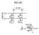
- Figure 10b is a view showing four memory cells of the array of Fig. 10a.
- a bias voltage of about -20 V is applied to a word line WL1 connected to the cell 1 and a bias voltage of about +8 V to a bit line BL1 connected to the cell 1.
- the carrier traps 13 in the gate insulation film 14 of the cell 1 capture carriers to establish a written state.
- a bias voltage of about 0 V is applied to a word line WL2 and a bit line BL2, so that no writing or erasing voltage may be applied to other cells 2, 3 and 4. Namely, the cells 2, 3 and 4 are not written or erased, while the cell 1 is uniquely selected among the cells 1 to 4 and written.
- a bias voltage of about -6 V is applied to the word line WL1 and a bias voltage of about +2 V to the bit line BL1. Since the cell 1 is holding the carriers, a tunneling current (Id) flowing between the substrate 11 and drain region 12 of the cell 1 will be about 10 ⁇ 12 A with respect to a gate voltage (Vg) of about -6 V, as shown in Fig. 6. This current is read through the bit line BL1. If the cell 1 is holding no carriers, the tunneling current Id will be about 5x10 ⁇ 9 A with respect to the gate voltage Vg of about -6 V. This current is read through the bit line BL1. Bv detecting the difference of the current, information stored in the call 1 is known.
- a bias voltage of about 0 V is applied to the word line WL2 and bit line BL2, so that only the cell 1 is read.
- a bias voltage of about 20 V is applied to the word lines WL1 and WL2 to release carriers captured by the carrier traps 13 in the gate insulation films 14 of the cells 1 to 4.
- each memory cell according to the embodiment comprises only one high-concentration impurity region and only one gate electrode on a semiconductor substrate. This can provide a very small nonvolatile memory cell capable of being electrically written, read and erased, smaller than a usual MOSFET.
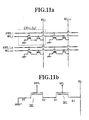
- FIGS 11a and 11b show an array of nonvolatile memory cells arranged in a matrix according to the embodiment.
- a memory cell (i, j) comprises a first MOSFET M1 and a second MOSFET M2 connected in series between a bit line BLj and a reference voltage (a ground voltage in this embodiment).
- a gate electrode of the first MOSFET is connected to a word line WLi
- a gate electrode of the second MOSFET is connected to a second word line SWLi.
- the first MOSFET M1 is a select gate transistor
- the second MOSFET M2 is an information storage element.
- the second MOSFET M2 of fig. 11b must be a transistor whose threshold voltage can be decreased by changing its effective channel length.
- This transistor can be realized by controlling basic parameters that determine a structure of the MOSFET.
- the parameters include a gate oxide film thickness Tox, a substrate concentration Nsub, a junction depth xj of source and drain diffusion layer, etc.
- the threshold voltage of the transistor is constant when the channel length is equal to or greater than 0.5 ⁇ m.
- the threshold voltage rapidly decreases.
- the threshold voltage changes before and after capturing carriers. From these facts, the channel length is set to 0.4 ⁇ m or smaller for the above parameters. If the channel length is too short, carriers captured in the oxide film do not sufficiently act on the characteristics of the element.
- the channel length is, therefore, preferable to be about 0.4 ⁇ m in this embodiment to provide a sufficient short channel effect.
- the second MOSFET is formed based on parameters expressed with the following equation.
- a channel length of the second MOSFET is set to the above Lmin.
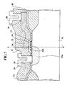
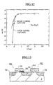
- Figure 13 is a sectional view of the first MOSFET M1 and second MOSFET M2 of Fig. 11.
- a film thickness of the gate oxide film of the transistor is, for example, 25 nm, a concentration of the substrate 4x1016 cm ⁇ 3, and a channel length 0.4 ⁇ m.
- a source S1 of the first MOSFET is common with a drain D2 of the second MOSFET to realize a compact memory cell.
- a gate G1 of the first MOSFET M1 i.e., the select transistor of a selected memory cell is turned ON to establish a conductive state.
- a voltage of 5V is applied to the drain D2, thereby generating an inter-band tunneling current in an overlap region of the gate and drain. This generates carriers 130, which are captured in the oxide film. Whether or not the carriers are captured in the oxide film corresponds to information "1" or "0.”
- the MOSFET incorporating a large number of the carrier traps, for example, about 5x1012 cm ⁇ 2 is formed as follows:
- a gate oxide film is formed, and a substrate is annealed in a nitrogen atmosphere. For example, the annealing is carried out for 60 minutes at 1000 degrees centigrade in the nitrogen atmosphere. Thereafter, the usual manufacturing processes are employed to form the MOSFET. Through the annealing process carried out after the formation of the gate oxide film, the carrier traps of about 5x1012 cm ⁇ 2 are formed in the gate oxide film.
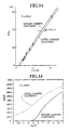
- a memory device formed with the above-mentioned MOSFETs can store information with no floating gates. Due to this, manufacturing processes can be simplified. Figures 12, 14 and 15 show changes in characteristics of the MOSFET that is produced through the above processes and captures carriers in its oxide film.
- Figure 12 shows the dependency of a threshold voltage on a channel length of the MOSFET in a triode region with the gate insulation film holding carriers.
- the carriers captured in the gate insulation film cause the short channel effect.
- Figure 14 shows an inverse of a maximum value of transconductance Gm ( ⁇ Id/ ⁇ Vg) in the triode region of the MOSFET with the gate insulation film holding or not holding carriers. It is understood that an effective channel length is reduced by 0.1 ⁇ m due to the captured carriers.
- Figure 15 shows changes in current-voltage characteristics before and after the oxide film capturing carriers.
- the captured carriers shorten the effective channel length and decrease a threshold of the MOSFET, thereby increasing a drain current for the same gate voltage.
- a current driving force differs depending on whether or not the oxide film is capturing carriers. Based on the difference of the current driving force, information of "1" or "0" can be discriminated.
- a positive bias for example, 20 V is applied to the gate G2 of Fig. 13, thereby discharging the carriers 130 captured by the carrier traps in the oxide film.
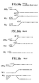
- Figures 16a to 16c are views showing control signals that are used for writing, erasing and reading data to and from the memory cell of Fig. 11.
- Figure 16a corresponds to a writing operation.
- the potential of a corresponding second word line SWLi is changed, for example, from 0 V to 15 V.
- the potential of a word line WLi of the gate of the first MOSFET is changed, for example, from 0 to 8 V to turn ON the select gate of the first MOSFET M1.
- the potential of a bit line BLj is changed, for example, from 0 to 5 V.
- the second MOSFET M2 whose gate voltage on the second word line SWLi is -15 V and drain voltage on the bit line 5 V causes an apparent inter-band tunneling current in a gate-drain overlap region.
- a zero bias voltage is commonly applied to the source, drain and substrate, and a positive bias voltage of, for example, 20 V is applied to the gate.
- a potential of the word line WLi is changed, for example, from 0 to 8 V to turn ON the select gate transistor M1.
- a potential of the second word line SWLi is changed from 0 to 20 V. According to this operation, data of memory cells connected to the second word line SWLi can simultaneously be erased.
- a data reading operation wilL be explained with reference to Fig. 16c.
- the bit line BLj is precharged to, for example, 5 V.
- a potential of the second word line SWLi is changed, for example, from 0 to a threshold voltage Vth that is of a transistor not holding carriers.
- a potential of the word line WLi is changed, for example, from 0 to 8 V, As a result, when the oxide film of the second MOSFET of the cell (i, j) is holding carriers, the potential of the bit line is reduced by a large current.
- the potential of the bit line is decreased a little by a smaller current. Namely, depending on whether or not the gate oxide film of the second MOSFET is holding the carriers, a change in the potential of the bit line greatly differs. After a certain period of time, the change in the potential of the bit line is amplified by a sense amplifier to discriminate the contents ("1" or "0") of the memory cell. During this reading operation, the carriers captured in the gate oxide film of the second MOSFET are not released from the carrier traps, so that data can be read non-destructively.
- this embodiment employs only MOSFETS produced through usual MOSFET manufacturing processes, so that the embodiment can provide, at a low cost, a nonvolatile memory cell that is capable of being electrically written, read and erased.
Landscapes
- Engineering & Computer Science (AREA)
- Microelectronics & Electronic Packaging (AREA)
- Non-Volatile Memory (AREA)
- Semiconductor Memories (AREA)
Abstract
Description
- The present invention relates to a nonvolatile memory cell that is capable of being electrically written, read and erased depending on carriers captured by or released from carrier traps formed in a gate insulation film of the memory cell. It also relates to a method of manufacturing the nonvolatile memory cell.
- A known nonvolatile memory device capable of being electrically written, read and erased is an EEPROM.
- Figures 1a and 1b show a memory cell comprising a transistor having a floating gate, of the EEPROM. To erase the contents of the memory cell in Fig. 1a, a bias voltage of about, for example, 20 V is applied to a
control gate 4 and a bias voltage of about 0 V to adrain region 2 formed on asemiconductor substrate 1, thereby injecting electrons from thedrain region 2 into afloating gate 3. - To write the memory cell in Fig. 1b, a bias voltage of about 0 V is applied to the
control gate 4 and a bias voltage of about 20 V to thedrain region 2, thereby releasing electrons from thefloating gate 3 toward thedrain region 2. - Figure 2 shows a memory device comprising a matrixed array of memory cells each including only the above-mentioned transistor.
- To write a
cell 1 in Fig. 2, a bias voltage of about 0 V is applied to a word line WL1 and a bias voltage of about 20 V to a bit line BL1, thereby establishing a write state of thecell 1. - Due to the bias voltage of about 20 V on the bit line BL1, a
cell 3 will be written if a bias voltage of about 0 V is applied to a word line WL2. To avoid this, a bias voltage of about 20 V is applied to the word line WL2. Also, due to the bias voltage of about 0 V on the word line WL1, acell 2 will be written if a bias voltage of about 20 V is applied to a bit line BL2. To avoid this, a bias voltage of about 0 V is applied to the bit line BL2. - With the word line WL1 being provided with 0 V, word line WL2 with 20 V, bit line BL1 with 20 V and bit line BL2 with 0 V, a
cell 4 receives the bias voltage of about 0 V through its drain region and the bias voltage of about 20 V through its control gate, as shown in Fig. 1a. As a result, thecell 4 will be erased to lose information stored therein. - In this way, if each memory cell includes only the transistor of Fig. 1, the memory cells may interact with one another. It is then impossible to select only one of the memory cells to write or erase the one.
- To prevent such interactions of memory cells, "Proc of the 4th on Solid State Devices, Tokyo, 1972" (p. 158) by Iizuka et al. discloses a structure of Fig. 3. According to this, each memory cell comprises a
transistor 6 with a floating gate, and atransfer transistor 5. Thetransistors transfer transistors 5, it is possible to select only one memory cell to write or erase the one. - The structure of Fig. 3, however, needs two transistors for each memory cell.
- As explained above, the electrically writable and erasable nonvolatile memory cells each composed of a single transistor having a floating gate interact with one another, so that it is impossible to select and write or erase each of the cells.
- On the other hand, the arrangement with the transfer transistors requires two elements for each memory cell, thereby increasing an area of each cell to hinder high integration.
- In addition, the nonvolatile memory cell having the floating gate requires complicated manufacturing processes compared with a normal MOSFET, due to the floating gate. This increases manufacturing costs.
- To solve the problems, an object of the present invention is to provide a novel nonvolatile memory cell that is capable of being electrically written, read and erased according to carriers captured by or released from carrier traps formed in a gate insulation film of the memory cell, and a method of manufacturing this sort of nonvolatile memory cell.
- Another object of the present invention is to provide an array of nonvolatile memory cells capable of being selectively written, read and erased, occupying a small area for the sake of high integration, and being simple to manufacture.
- In order to accomplish the objects, the present invention provides a nonvolatile memory cell comprising a semiconductor substrate of first conduction type, a high-concentration impurity region of second conduction type formed on the semiconductor substrate and connected to a bit line, an insulation film in which carrier traps are formed, and a gate electrode that is opposite the high-concentration impurity region across the insulation film and connected to a word line. Carriers are captured by and released from the carrier traps formed in the insulation film, in response to bias voltages applied to the word and bit lines. Information stored in the memory cell depends on whether or not the carrier traps are holding carriers, and the information is read out of the memory cell as the difference of a tunneling current flowing between the semiconductor substrate and the high-concentration impurity region.
- According to this arrangement, an amount of the tunneling current flowing between the semiconductor substrate and the high-concentration impurity region in an area where the gate electrode faces the high-concentration impurity region is controlled according to the strength of a vertical electric field that changes depending on carriers captured by or released from the carrier traps formed in the area. Namely, an information storage function of the memory cell is realized by the tunneling current that drastically changes depending on whether or not the carrier traps are holding the carriers.
- In the above arrangement, the amount of the tunneling current controlled by the magnitude of the vertical electric field is influenced by the side of a band gap of the high-concentration impurity region that is facing the gate electrode. To secure a sufficient amount of the tunneling current, it is possible to embed a material to the high-concentration impurity region to form a region that has a different band gap, and flow the tunneling current through the region.
- The present invention also provides a memory cell comprising a first MOSFET acting as a select transistor and a second MOSFET for storing information. The first and second MOSFETs are connected in series. To store information, an effective channel length of the second MOSFET is reduced. This increases a short channel effect, decreases a threshold voltage, and drastically changes current-voltage characteristics of the second MOSFET, thereby storing the information in the second MOSFET. A gate insulation film of the second MOSFET includes carrier traps, and depending on whether or not the carrier traps are holding carriers, the current-voltage characteristics of the second MOSFET change drastically.
- These and other objects, features and advantages of the present invention will be more apparent from the following detailed description of preferred embodiments in conjunction with the accompanying drawings.
-
- Figs. 1a and 1b are explanatory views showing an operation of a conventional EEPROM;
- Fig. 2 is a view showing an arrangement of memory cells of the conventional EEPROM;
- Fig. 3 is a view showing a memory cell of another conventional EEPROM;
- Fig. 4 is a sectional view showing a nonvolatile memory cell according to an embodiment of the present invention;
- Figs. 5a to 5d are sectional views showing manufacturing processes of the memory cell of Fig 4;
- Fig. 6 is a voltage-current characteristic diagram showing the memory cell of Fig. 4;
- Fig. 7 is a sectional view showing a nonvolatile memory cell involving a material, which has a different band gap from the peripheral area, at a part where a tunneling current flows, according to another embodiment of the present invention;
- Fig. 8a is a sectional view showing a nonvolatile memory cell, Figs. 8b and 8c are views showing a band structure along a line A-A′ of Fig. 7;
- Figs. 9a to 9c are sectional views showing manufacturing processes of the memory cell of Fig. 7;
- Fig. 10a is a view showing an array of memory cells each of Fig. 4 or 8;
- Fig. 10b is a view showing four cells among the array of Fig. 10a;
- Figs. 11a and 11b are circuit diagrams showing a nonvolatile memory cell according to still another embodiment of the present invention;
- Fig. 12 is a graph showing the dependency of a threshold on a channel length of a MOSFET with a gate oxide film of the MOSFET capturing or not capturing positive holes;
- Fig. 13 is a sectional view showing the MOSFETS of the memory cell of Fig. 11b;
- Fig. 14 is a graph showing an inverse of a measured maximum value of transconductance Gm (δId/δVg) at a triode region of a MOSFET and a channel length of the MOSFET with carrier traps of a gate oxide film of the MOSFET capturing or not capturing positive holes;
- Fig. 15 is a view showing the characteristics of drain current and gate voltage at a triode region of the second MOSFET (M2) of the memory cell of Fig. 11b with a gate oxide film of the MOSFET capturing or not capturing positive holes; and
- Figs. 16a to 16c are views showing waveforms of writing, erasing and reading operations of the memory cell of Fig. 11b.
- Figure 4 is a sectional view showing a nonvolatile memory cell according to the embodiment of the present invention. This embodiment involves a PN junction formed on a semiconductor substrate, and a gate electrode formed at the PN junction to realize a nonvolatile storage function.
- In Fig. 4, a
silicon semiconductor substrate 11 is of, for example, P type. N-type impurities such as arsenic impurities of 5x10¹⁸ cm⁻³ or over are implanted to the surface of thesubstrate 11 to form a high-concentration impurity region (a drain region) 12. Thedrain region 12 andsubstrate 11 form the PN junction. - A
gate insulation film 14 such as a silicon oxide film is formed on thesubstrate 11. Carrier traps (hole traps) 13 of about 5x10¹² cm⁻² are formed in thegate insulation film 14. Agate electrode 15 of polycrystalline silicon is formed on thegate insulation film 14. Thegate electrode 15 partly faces thedrain region 12 across thegate insulation film 14. - An
insulation film 16 is formed over thedrain region 12 andgate electrode 15. Contact holes 17a and 17b are formed through theinsulation film 16, and adrain wire 18 and agate electrode wire 19 are connected to thedrain region 12 andgate electrode 15 through thecontact holes - The above arrangement forms one memory cell which is separated from adjacent memory cells by an
element separation region 20. - A method of manufacturing the memory cell of Fig. 4 will be explained with reference to Figs. 5a to 5d.
- In Fig. 5a, a P-
type silicon substrate 11 having impurities of, for example, 1x10¹⁶ cm⁻³ is selectively oxidized to form anelement separation region 20 around an area where a memory cell is to be formed. - The surface of the
substrate 11 is thermally oxidized at a temperature of about 900 degrees centigrade to form agate insulation film 14, i.e., a silicon oxide film of about 250 angstroms in thickness. On thegate insulation film 14, apolycrystalline silicon layer 21 is deposited to a thickness of about 3000 angstroms by, for example, a CVD method. Thelayer 21 will be agate electrode 15. Phosphorus impurities are implanted and diffused to thepolycrystalline silicon layer 21 to about 1x10²⁰ cm⁻³ in concentration. Thelayer 21 is then coated with resist. The resist is patterned to a resistpattern 22 of Fig. 5b on a part of thelayer 21 where thegate electrode 15 is formed. - The resist
pattern 22 is used an a mask, and thepolycrystalline silicon layer 21 is partly etched and removed by, for example, an RIE method, thereby forming thegate electrode 15. The material is then annealed for about 60 minutes in a nitrogen atmosphere at about 1000 degrees centigrade. This forms carrier traps (hole traps) 13 of about 5x10¹² cm⁻² in thegate insulation film 14. Impurities such as arsenic of about 1x10¹⁵ cm⁻² are ion-implanted to thesubstrate 11 at energy of about 160 keV, thereby forming, in a self-aligning manner, a high-concentration impurity region (a drain region) 12 on the surface of thesubstrate 11. Thereafter, thermal diffusion is carried out on the material for about 30 minutes at about 900 degrees centigrade. This activates the impurities in the high-concentration impurity region 12, cures damages caused by the ion implantation, and horizontally diffuses the impurities, thereby completing the high-concentration drain region 12. A part of thedrain region 12 faces thegate electrode 15 across thegate insulation film 14. Aninsulation film 16 is then deposited over the material by, for example, the CVD method to a thickness of about 3000 angstroms, as shown in Fig. 5c. - Contact holes 17a and 17b are opened through the
insulation film 16 to reach thegate electrode 15 and drainregion 12, respectively. Adrain wire 18 and agate electrode wire 19 both made of, for example, aluminum are arranged through thecontact holes - An operation of the memory cell will be explained.
- A current flowing between the
substrate 11 and thedrain region 12 changes depending on applied bias voltages. The changes in the current are related to binary information, thereby realizing a storage function of the memory cell. - The current flowing between the
substrate 11 and thedrain region 12 mainly passes an area where thedrain region 12 faces thegate electrode 15 with thegate insulation film 14 being between them. This current is a tunneling current generated by electrons that tunnel an interface between thedrain region 12 and thegate insulation film 14 from a valence band to a conduction band (inter-band tunneling). This inter-band tunneling current occurs in an overlap area of the high-concentration drain region and gate, and is described in, for example, "IEEE Electron Device Letters" Vol. EDL-8, No. 11, November 1987, pp. 515 to 517. - The tunneling current is expressed as follows with respect to a vertical electric field produced at the interface between the silicon substrate and the gate insulation film:
Id = A x Ex x exp (-B/Es)
where Id is the tunneling current, A and B constants, and Es the vertical electric field at the interface between the silicon substrate and the gate insulation film. As is apparent from the above equation, the tunneling current Id drastically changes depending on changes in the vertical electric field Es. According to the present invention, the carrier traps 13 formed in thegate insulation film 14 in the area where the tunneling current occurs and where thedrain region 12 faces thegate electrode 15 capture carriers, which then change the vertical electric field. - Figure 6 is a graph showing relations of an inter-band tunneling current and a gate voltage of the memory cell formed on the P-
type substrate 11, before and after the carrier traps 13 capture carriers. - In Fig. 6, the number of the carrier traps is about 5x10¹² cm⁻². When a bias voltage of about 0 V is applied to the
substrate 11 and a bias voltage of about 2 V to thedrain region 12, no carrier is captured by the carrier traps. When a bias voltage of about -8 V is applied to thesubstrate 11 and a bias voltage of about -20 V to thegate electrode 15, carriers are captured by the carrier traps 13 in thegate insulation film 14. Measured values of the gate voltage Vg and tunneling current Id of the carrier-not-captured state and carrier-captured state are shown in Fig. 6. - In the area where the
drain region 12 faces thegate electrode 15 across thegate insulation film 14, the inter-band tunneling phenomenon produces electron-hole pairs. Among the pairs, the holes run on the interface between thesubstrate 11 and thegate insulation film 14 and some of them surmount an energy barrier between thesilicon substrate 11 and the gate insulation film (silicon oxide film) 14, because the holes receive sufficient energy from an electric field produced by the bias voltages. And the holes are captured as captured carriers by the carrier traps 13 in thefilm 14. - As is apparent from Fig. 6, a value of the gate voltage Vg at which the tunneling current starts to increase shifts by about 6 V before and after the carrier capturing. A value of the tunneling current Id with the gate voltage being about -6 V changes by about 10⁴ times before and after the carrier capturing.
- In this way, the tunneling current drastically changes in response to the carrier capturing/releasing, i.e., the strength of the vertical electric field in the area where the tunneling current occurs. These changes of the current are related to binary information, thereby realizing the information storing function of the memory cell.
- To write the memory cell, a bias voltage of about -20 V is applied to the
gate electrode 15 and a bias voltage of about -8 V to thesubstrate 11, so that the carrier traps 13 capture carriers. At this time, if the bias voltage is applied to only one of thegate electrode 15 andsubstrate 11, the carrier traps 13 do not capture the carriers. This means that any memory cell can uniquely be selected to write. - To erase the memory call, the carriers captured by the carrier traps 13 are released to reestablish the carrier-not-captured state. To do so, a positive voltage of about 20 V, for example, is applied to the
gate electrode 15. - Figure 7 shows another embodiment of the present invention.
- In Fig. 7, a nonvolatile memory cell comprises a high-concentration region formed in a semiconductor substrate, a PN junction formed between the high-concentration region and the substrate, and a gate electrode. To increase the tunneling current, this embodiment embeds a material to a part of the high-concentration region where the inter-band tunneling occurs to provide the part with a different band gap.
- Similar to the embodiment of Fig. 4, the memory cell of Fig. 7 comprises, for example, a P-type
silicon semiconductor substrate 31. N-type impurities such as phosphorus of 5x10¹⁸ cm⁻³ or over are implanted to the surface of thesubstrate 31 to form a high-concentration impurity region (a drain region) 32a. Thedrain region 32a and awell region 31 form a PN junction. Agate insulation film 34 made of, for example, a silicon oxide film is formed on thesubstrate 31. Carrier traps 33 of about 5x10¹² cm⁻² are formed in the gate insulation film 94. Agate electrode 35 made of, for example, aluminum is formed on thegate insulation film 34. Thedrain region 32a andgate electrode 35 partly face each other across thegate insulation film 34. - Material such as mixed crystals of germanium and silicon that provides a different band gap is embedded to an
area 36 of thedrain region 32a where the inter-band tunneling occurs. Aninsulation film 37 is entirely deposited. Contact holes 38 reaching thedrain region 32a andgate electrode 35, respectively, are formed through theinsulation film 37, and adrain wire 39 and agate electrode wire 40 are connected to thedrain region 32a andgate electrode 35, respectively, through the contact holes 38. - The above arrangement forms one memory cell, which is separated by an
element separation region 41 from adjacent memory cells. - An affect of the
area 36 having the different band gap in the structure of Fig. 7 on the tunneling current will be explained with reference to Figs. 8a to 8c. Figure 8a is a sectional view showing the structure of Fig. 7, and Figs. 8b and 8c show bands on a path of the tunneling current - In an area where the
drain region 32a faces thegate electrode 35 across thegate insulation film 34, thegate electrode 35 applies a strong bias to greatly bend a valence band and a conduction band, and electrons tunnel from the valence band to the conduction band. The electrons cause a tunneling current flowing between thesubstrate 31 and thedrain region 32a. Supposing an interface level at a heterojunction is ignorable, the tunneling current can be evaluated as follows:
Id = AXexp(-B V(x)-k²) (1)
where Id is the tunneling current, A and B constants, V(x) a potential barrier against electrons in a tunnel path, x0 and x1 ends of the potential barrier, and k a constant determined by the energy of the tunneling electrons. - In the equation (1), the tunneling current Id depends on the height and width of the potential barrier against the tunneling electrons. As the band gap of semiconductor at the tunneling part becomes smaller, the height of the barrier becomes lower and the width thereof narrower. Accordingly, if the tunneling part is made of material that can reduce the integration of the exponential part of the equation (1), the inter-band tunneling current can be increased. If there is an unignorable interface level, it generates a tunneling current in addition to the one expressed by the equation (1), thereby further increasing the tunneling current. If these conditions are optimized, a sufficient tunneling current is obtainable.
- Manufacturing processes of the structure of Fig. 7 will be explained with reference to Figs. 9a to 9c.
- A P-type silicon substrate with impurity concentration of about 1x10¹⁶ cm⁻³ is prepared. A usual selective oxidizing method is used to form an
element separation region 41 made of a nitride film around a region where a memory cell is to be formed. (Fig. 9a) - The nitride film on an area where a
drain region 32a is to be formed is removed. The remaining nitride film is used as a mask, and, for example, phosphorus of about 1x10¹⁵ cm⁻² is ion-implanted to the substrate and thermally diffused for about 30 minutes at 900 degrees centigrade, thereby activating the implanted phosphorus. The nitride film is then removed. Hydrogen diluted SiCl₂H₂, GeH₄ and PH₃ are used to epitaxially grow, for example, an N-type Si0.69Ge0.31 mixed crystal layer of, for example, 50 angstroms in thickness under a pressure of 6 torrs at 640 degrees centigrade. Thereafter, an N-type Si layer of, for example, 50 angstroms in thickness is grown at 850 degrees centigrade. An RIE method is employed to remove the epitaxial layers that the epitaxial layers remain partly on thedrain region 32a, thereby forming thedrain region 32a having anarea 36 that has a different band gap. (Fig. 9b) - A plasma enhanced CVD is employed to form a gate oxide film (a gate insulation film) 34 having carrier traps 33 at 550 degrees centigrade. Aluminum, for example, is deposited by a CVD method, and etched by the RIE method to form a
gate electrode 35 that partly faces thedrain region 32a. Aninsulation film 37 is entirely deposited by, for example, the CVD method to a thickness of about 3000 angstroms. Contact holes 38 reaching thegate electrode 39 and drainregion 32a, respectively, are formed through theinsulation film 37, and agate electrode wire 39 and adrain wire 40 made of, for example, aluminum are formed through the contact holes 38, thereby completing the memory cell of Fig. 9c. - The memory cells of Fig. 4 or Fig. 7 are arranged in a matrix similar to a usual semiconductor memory, and a word line decoder, sense amplifier, bit line decoder, etc., are arranged to form a memory such as one shown in Fig. 10a.
- Figure 10b is a view showing four memory cells of the array of Fig. 10a.
- To write a
cell 1 of Fig. 10b, a bias voltage of about -20 V is applied to a word line WL1 connected to thecell 1 and a bias voltage of about +8 V to a bit line BL1 connected to thecell 1. As a result, the carrier traps 13 in thegate insulation film 14 of thecell 1 capture carriers to establish a written state. - Meantime, a bias voltage of about 0 V is applied to a word line WL2 and a bit line BL2, so that no writing or erasing voltage may be applied to
other cells cells cell 1 is uniquely selected among thecells 1 to 4 and written. - To read the
cell 1, a bias voltage of about -6 V is applied to the word line WL1 and a bias voltage of about +2 V to the bit line BL1. Since thecell 1 is holding the carriers, a tunneling current (Id) flowing between thesubstrate 11 and drainregion 12 of thecell 1 will be about 10⁻¹² A with respect to a gate voltage (Vg) of about -6 V, as shown in Fig. 6. This current is read through the bit line BL1. If thecell 1 is holding no carriers, the tunneling current Id will be about 5x10⁻⁹ A with respect to the gate voltage Vg of about -6 V. This current is read through the bit line BL1. Bv detecting the difference of the current, information stored in thecall 1 is known. - During the reading operation of the
cell 1, a bias voltage of about 0 V is applied to the word line WL2 and bit line BL2, so that only thecell 1 is read. - To erase the
cells 1 to 4, a bias voltage of about 20 V is applied to the word lines WL1 and WL2 to release carriers captured by the carrier traps 13 in thegate insulation films 14 of thecells 1 to 4. - As explained above, each memory cell according to the embodiment comprises only one high-concentration impurity region and only one gate electrode on a semiconductor substrate. This can provide a very small nonvolatile memory cell capable of being electrically written, read and erased, smaller than a usual MOSFET.
- Still another embodiment of the present invention will be explained.
- Figures 11a and 11b show an array of nonvolatile memory cells arranged in a matrix according to the embodiment. A memory cell (i, j) comprises a first MOSFET M1 and a second MOSFET M2 connected in series between a bit line BLj and a reference voltage (a ground voltage in this embodiment). A gate electrode of the first MOSFET is connected to a word line WLi, and a gate electrode of the second MOSFET is connected to a second word line SWLi. The first MOSFET M1 is a select gate transistor, and the second MOSFET M2 is an information storage element.
- The second MOSFET M2 of fig. 11b must be a transistor whose threshold voltage can be decreased by changing its effective channel length. This transistor can be realized by controlling basic parameters that determine a structure of the MOSFET. The parameters include a gate oxide film thickness Tox, a substrate concentration Nsub, a junction depth xj of source and drain diffusion layer, etc.
- Figure 12 is a graph showing the dependency of a threshold voltage on a channel length L of a MOSFET of Tox=25nm, Nsub=4x10¹⁶ cm⁻³ and xj=0.2µm. In the graph, the threshold voltage of the transistor is constant when the channel length is equal to or greater than 0.5 µm. When the channel length is equal to or smaller than 0.4 µm, the threshold voltage rapidly decreases. In addition, the threshold voltage changes before and after capturing carriers. From these facts, the channel length is set to 0.4 µm or smaller for the above parameters. If the channel length is too short, carriers captured in the oxide film do not sufficiently act on the characteristics of the element. The channel length is, therefore, preferable to be about 0.4 µm in this embodiment to provide a sufficient short channel effect.
- The second MOSFET is formed based on parameters expressed with the following equation. A miminum channel length Lmin at which the short channel effect is apparent is described in IEEE Electron Device Lett. EDL-1, p. 2 (1980) by J.R. Brews, in. Fiochtener, E.H. Nicollian, and S.Mx Sze, as follows:
Lmin = 0.4ν1/3
where ν = xj.Tox.2ε₂(2Vbi+Vd)/q.NA
and Vbi is a built-in potential between source/drain and substrate. A channel length of the second MOSFET is set to the above Lmin. - A method of writing (storing) information to the memory cell of Fig. 11 will be explained. Figure 13 is a sectional view of the first MOSFET M1 and second MOSFET M2 of Fig. 11. Here, a film thickness of the gate oxide film of the transistor is, for example, 25 nm, a concentration of the substrate 4x10¹⁶ cm⁻³, and a channel length 0.4 µm. A source S1 of the first MOSFET is common with a drain D2 of the second MOSFET to realize a compact memory cell. To write information to the memory cell, a gate G1 of the first MOSFET M1, i.e., the select transistor of a selected memory cell is turned ON to establish a conductive state. A source 52 oF the second MOSFET is grounded, and a negative bias Vg=-15 V is applied to a gate G2. At the same time, a voltage of 5V is applied to the drain D2, thereby generating an inter-band tunneling current in an overlap region of the gate and drain. This generates carriers 130, which are captured in the oxide film. Whether or not the carriers are captured in the oxide film corresponds to information "1" or "0."
- The MOSFET incorporating a large number of the carrier traps, for example, about 5x10¹² cm⁻² is formed as follows:
- In usual MOSFET manufacturing processes, a gate oxide film is formed, and a substrate is annealed in a nitrogen atmosphere. For example, the annealing is carried out for 60 minutes at 1000 degrees centigrade in the nitrogen atmosphere. Thereafter, the usual manufacturing processes are employed to form the MOSFET. Through the annealing process carried out after the formation of the gate oxide film, the carrier traps of about 5x10¹² cm⁻² are formed in the gate oxide film.
- A memory device formed with the above-mentioned MOSFETs can store information with no floating gates. Due to this, manufacturing processes can be simplified. Figures 12, 14 and 15 show changes in characteristics of the MOSFET that is produced through the above processes and captures carriers in its oxide film.
- Figure 12 shows the dependency of a threshold voltage on a channel length of the MOSFET in a triode region with the gate insulation film holding carriers. The carriers captured in the gate insulation film cause the short channel effect.
- Figure 14 shows an inverse of a maximum value of transconductance Gm (δId/δVg) in the triode region of the MOSFET with the gate insulation film holding or not holding carriers. It is understood that an effective channel length is reduced by 0.1 µm due to the captured carriers.
- Figure 15 shows changes in current-voltage characteristics before and after the oxide film capturing carriers. The captured carriers shorten the effective channel length and decrease a threshold of the MOSFET, thereby increasing a drain current for the same gate voltage. A current driving force differs depending on whether or not the oxide film is capturing carriers. Based on the difference of the current driving force, information of "1" or "0" can be discriminated.
- To erase the information stored in MOSFET, a positive bias, for example, 20 V is applied to the gate G2 of Fig. 13, thereby discharging the carriers 130 captured by the carrier traps in the oxide film.
- Figures 16a to 16c are views showing control signals that are used for writing, erasing and reading data to and from the memory cell of Fig. 11.
- Figure 16a corresponds to a writing operation. When the cell (i, j) of Fig. 11 is to be written, the potential of a corresponding second word line SWLi is changed, for example, from 0 V to 15 V. At substantially the same timing, the potential of a word line WLi of the gate of the first MOSFET is changed, for example, from 0 to 8 V to turn ON the select gate of the first MOSFET M1. Thereafter, the potential of a bit line BLj is changed, for example, from 0 to 5 V. At this time, the second MOSFET M2 whose gate voltage on the second word line SWLi is -15 V and drain voltage on the bit line 5 V causes an apparent inter-band tunneling current in a gate-drain overlap region. As a result, carriers are injected into the oxide film and captured by the carrier traps. If the select gate of the first MOSFET is in an OFF state, the corresponding memory cell is in an unselected state Accordingly, only the second MOSFET M2 of the cell (i, j) can capture carriers in its gate oxide film.
- An erasing operation will be explained with reference to Fig. 16b. To discharge the carriers captured in the oxide film of the second MOSFET M2, a zero bias voltage is commonly applied to the source, drain and substrate, and a positive bias voltage of, for example, 20 V is applied to the gate. As shown in Fig. 16b, a potential of the word line WLi is changed, for example, from 0 to 8 V to turn ON the select gate transistor M1. Thereafter, a potential of the second word line SWLi is changed from 0 to 20 V. According to this operation, data of memory cells connected to the second word line SWLi can simultaneously be erased.
- A data reading operation wilL be explained with reference to Fig. 16c. To read data from the cell (i, j), the bit line BLj is precharged to, for example, 5 V. Thereafter, a potential of the second word line SWLi is changed, for example, from 0 to a threshold voltage Vth that is of a transistor not holding carriers. A potential of the word line WLi is changed, for example, from 0 to 8 V, As a result, when the oxide film of the second MOSFET of the cell (i, j) is holding carriers, the potential of the bit line is reduced by a large current. On the other hand, if the second MOSFET of the cell (i, j) is not holding the carriers, the potential of the bit line is decreased a little by a smaller current. Namely, depending on whether or not the gate oxide film of the second MOSFET is holding the carriers, a change in the potential of the bit line greatly differs. After a certain period of time, the change in the potential of the bit line is amplified by a sense amplifier to discriminate the contents ("1" or "0") of the memory cell. During this reading operation, the carriers captured in the gate oxide film of the second MOSFET are not released from the carrier traps, so that data can be read non-destructively.
- As described above, this embodiment employs only MOSFETS produced through usual MOSFET manufacturing processes, so that the embodiment can provide, at a low cost, a nonvolatile memory cell that is capable of being electrically written, read and erased.
- Various modifications will become possible for those skilled in the art after receiving the teachings of the present disclosure without departing from the scope thereof.
Claims (15)
Applications Claiming Priority (2)
| Application Number | Priority Date | Filing Date | Title |
|---|---|---|---|
| JP1249311A JPH03112167A (en) | 1989-09-27 | 1989-09-27 | Nonvolatile memory cell |
| JP249311/89 | 1989-09-27 |
Publications (3)
| Publication Number | Publication Date |
|---|---|
| EP0420182A2 true EP0420182A2 (en) | 1991-04-03 |
| EP0420182A3 EP0420182A3 (en) | 1993-01-07 |
| EP0420182B1 EP0420182B1 (en) | 1996-07-03 |
Family
ID=17191104
Family Applications (1)
| Application Number | Title | Priority Date | Filing Date |
|---|---|---|---|
| EP90118464A Expired - Lifetime EP0420182B1 (en) | 1989-09-27 | 1990-09-26 | Nonvolatile memory cell and its manufacturing method |
Country Status (3)
| Country | Link |
|---|---|
| EP (1) | EP0420182B1 (en) |
| JP (1) | JPH03112167A (en) |
| DE (1) | DE69027641T2 (en) |
Cited By (1)
| Publication number | Priority date | Publication date | Assignee | Title |
|---|---|---|---|---|
| CN105513984A (en) * | 2014-09-24 | 2016-04-20 | 北大方正集团有限公司 | Test method and device for practical channel length of MOS tubes |
Families Citing this family (1)
| Publication number | Priority date | Publication date | Assignee | Title |
|---|---|---|---|---|
| JP2965415B2 (en) * | 1991-08-27 | 1999-10-18 | 松下電器産業株式会社 | Semiconductor storage device |
Family Cites Families (5)
| Publication number | Priority date | Publication date | Assignee | Title |
|---|---|---|---|---|
| US3878549A (en) * | 1970-10-27 | 1975-04-15 | Shumpei Yamazaki | Semiconductor memories |
| DE2151508A1 (en) * | 1971-04-06 | 1972-10-12 | Robotron Veb K | Integrated semiconductor memory |
| US4037243A (en) * | 1974-07-01 | 1977-07-19 | Motorola, Inc. | Semi conductor memory cell utilizing sensing of variations in PN junction current conrolled by stored data |
| US3992701A (en) * | 1975-04-10 | 1976-11-16 | International Business Machines Corporation | Non-volatile memory cell and array using substrate current |
| FR2437046A2 (en) * | 1976-10-20 | 1980-04-18 | Texas Instruments France | FLOATING GRID MEMORY CELL |
-
1989
- 1989-09-27 JP JP1249311A patent/JPH03112167A/en active Pending
-
1990
- 1990-09-26 DE DE69027641T patent/DE69027641T2/en not_active Expired - Fee Related
- 1990-09-26 EP EP90118464A patent/EP0420182B1/en not_active Expired - Lifetime
Cited By (2)
| Publication number | Priority date | Publication date | Assignee | Title |
|---|---|---|---|---|
| CN105513984A (en) * | 2014-09-24 | 2016-04-20 | 北大方正集团有限公司 | Test method and device for practical channel length of MOS tubes |
| CN105513984B (en) * | 2014-09-24 | 2018-06-26 | 北大方正集团有限公司 | The test method and device of the actual channel length of metal-oxide-semiconductor |
Also Published As
| Publication number | Publication date |
|---|---|
| DE69027641D1 (en) | 1996-08-08 |
| JPH03112167A (en) | 1991-05-13 |
| EP0420182A3 (en) | 1993-01-07 |
| EP0420182B1 (en) | 1996-07-03 |
| DE69027641T2 (en) | 1996-12-05 |
Similar Documents
| Publication | Publication Date | Title |
|---|---|---|
| US5162880A (en) | Nonvolatile memory cell having gate insulation film with carrier traps therein | |
| US6552387B1 (en) | Non-volatile electrically erasable and programmable semiconductor memory cell utilizing asymmetrical charge trapping | |
| US6768165B1 (en) | Two bit non-volatile electrically erasable and programmable semiconductor memory cell utilizing asymmetrical charge trapping | |
| US5429965A (en) | Method for manufacturing a semiconductor memory | |
| US5402374A (en) | Non-volatile semiconductor memory device and memory circuit using the same | |
| US5768192A (en) | Non-volatile semiconductor memory cell utilizing asymmetrical charge trapping | |
| US6172905B1 (en) | Method of operating a semiconductor device | |
| EP0573170B1 (en) | Method of manufacture of high density EEPROM cell array | |
| US7485527B2 (en) | Nonvolatile semiconductor storage device and its manufacturing method | |
| US5361225A (en) | Nonvolatile memory device utilizing field effect transistor having ferroelectric gate film | |
| EP0915479A2 (en) | Nonvolatile semiconductor memory device and method of reading data therefrom | |
| US6768160B1 (en) | Non-volatile memory cell and method of programming for improved data retention | |
| US5477068A (en) | Nonvolatile semiconductor memory device | |
| JP4697993B2 (en) | Control method for nonvolatile semiconductor memory device | |
| US5589700A (en) | Semiconductor nonvolatile memory | |
| US6335549B1 (en) | EEPROM with high channel hot carrier injection efficiency | |
| TW200302569A (en) | Transistor and semiconductor memory using the same | |
| EP0420182A2 (en) | Nonvolatile memory cell and its manufacturing method | |
| JP3426643B2 (en) | Driving method of nonvolatile storage device | |
| JP3426641B2 (en) | Nonvolatile storage element, nonvolatile storage device using the same, and method of driving this storage device | |
| JP3469606B2 (en) | Nonvolatile storage element, nonvolatile storage device using the same, method of driving this storage device, and method of manufacturing this storage element | |
| JPH05110037A (en) | Semiconductor device | |
| JPH06314798A (en) | NONVOLATILE MEMORY ELEMENT, NONVOLATILE MEMORY DEVICE USING THE SAME, METHOD FOR DRIVING THE MEMORY DEVICE, AND METHOD FOR MANUFACTURING THIS MEMORY ELEMENT |
Legal Events
| Date | Code | Title | Description |
|---|---|---|---|
| PUAI | Public reference made under article 153(3) epc to a published international application that has entered the european phase |
Free format text: ORIGINAL CODE: 0009012 |
|
| 17P | Request for examination filed |
Effective date: 19900926 |
|
| AK | Designated contracting states |
Kind code of ref document: A2 Designated state(s): DE FR |
|
| PUAL | Search report despatched |
Free format text: ORIGINAL CODE: 0009013 |
|
| AK | Designated contracting states |
Kind code of ref document: A3 Designated state(s): DE FR |
|
| 17Q | First examination report despatched |
Effective date: 19940830 |
|
| GRAH | Despatch of communication of intention to grant a patent |
Free format text: ORIGINAL CODE: EPIDOS IGRA |
|
| GRAA | (expected) grant |
Free format text: ORIGINAL CODE: 0009210 |
|
| AK | Designated contracting states |
Kind code of ref document: B1 Designated state(s): DE FR |
|
| PG25 | Lapsed in a contracting state [announced via postgrant information from national office to epo] |
Ref country code: FR Free format text: THE PATENT HAS BEEN ANNULLED BY A DECISION OF A NATIONAL AUTHORITY Effective date: 19960703 |
|
| REF | Corresponds to: |
Ref document number: 69027641 Country of ref document: DE Date of ref document: 19960808 |
|
| GRAH | Despatch of communication of intention to grant a patent |
Free format text: ORIGINAL CODE: EPIDOS IGRA |
|
| EN | Fr: translation not filed | ||
| PLBE | No opposition filed within time limit |
Free format text: ORIGINAL CODE: 0009261 |
|
| STAA | Information on the status of an ep patent application or granted ep patent |
Free format text: STATUS: NO OPPOSITION FILED WITHIN TIME LIMIT |
|
| 26N | No opposition filed | ||
| PGFP | Annual fee paid to national office [announced via postgrant information from national office to epo] |
Ref country code: DE Payment date: 20070920 Year of fee payment: 18 |
|
| PG25 | Lapsed in a contracting state [announced via postgrant information from national office to epo] |
Ref country code: DE Free format text: LAPSE BECAUSE OF NON-PAYMENT OF DUE FEES Effective date: 20090401 |