EP0420267A2 - Appareil pour la production de dispositifs semiconducteurs - Google Patents
Appareil pour la production de dispositifs semiconducteurs Download PDFInfo
- Publication number
- EP0420267A2 EP0420267A2 EP90118679A EP90118679A EP0420267A2 EP 0420267 A2 EP0420267 A2 EP 0420267A2 EP 90118679 A EP90118679 A EP 90118679A EP 90118679 A EP90118679 A EP 90118679A EP 0420267 A2 EP0420267 A2 EP 0420267A2
- Authority
- EP
- European Patent Office
- Prior art keywords
- beds
- lead frame
- semiconductor devices
- bed
- injection
- Prior art date
- Legal status (The legal status is an assumption and is not a legal conclusion. Google has not performed a legal analysis and makes no representation as to the accuracy of the status listed.)
- Granted
Links
Images

Classifications
-
- H—ELECTRICITY
- H10—SEMICONDUCTOR DEVICES; ELECTRIC SOLID-STATE DEVICES NOT OTHERWISE PROVIDED FOR
- H10W—GENERIC PACKAGES, INTERCONNECTIONS, CONNECTORS OR OTHER CONSTRUCTIONAL DETAILS OF DEVICES COVERED BY CLASS H10
- H10W90/00—Package configurations
- H10W90/811—Multiple chips on leadframes
-
- H—ELECTRICITY
- H10—SEMICONDUCTOR DEVICES; ELECTRIC SOLID-STATE DEVICES NOT OTHERWISE PROVIDED FOR
- H10W—GENERIC PACKAGES, INTERCONNECTIONS, CONNECTORS OR OTHER CONSTRUCTIONAL DETAILS OF DEVICES COVERED BY CLASS H10
- H10W74/00—Encapsulations, e.g. protective coatings
- H10W74/01—Manufacture or treatment
- H10W74/016—Manufacture or treatment using moulds
Definitions
- the present invention relates generally to an apparatus for producing a plurality of resin molded semiconductor devices by an injection molding process. More particularly, the present invention relates to an improvement of the apparatus for producing a plurality of resin molded semiconductor devices wherein molten resin is injected into a plurality of die cavities on a lower die half while a plurality of semiconductor devices such as power hybrid integral circuits or the like each having different kinds of semiconductor elements, e.g., power transistors, diodes, integral circuits or the like mounted on plural kinds of beds each having a different area in a lead frame are placed in the die cavities on the lower die half.
- power hybrid integral circuits or the like each having different kinds of semiconductor elements, e.g., power transistors, diodes, integral circuits or the like mounted on plural kinds of beds each having a different area in a lead frame are placed in the die cavities on the lower die half.
- a transistor array of the type which is constructed such that a plurality of beds are arranged on a single lead frame, semiconductor elements are mounted on the beds while the lead frame is placed in the corresponding die cavity on a lower die half and molten resin is then injected into each of a plurality of die cavities has been heretofore known as a resin sealed type semiconductor device.
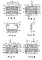
- This kind of transistor array is typically shown in Fig. 8.
- a lead frame 1 including a single kind of beds 3 each having a same area is used for the transistor array.
- the lead frame 1 is composed of a plurality of leads 2, a plurality of beds 3 each having same dimensions and an outer frame 4.
- a plurality of semiconductor elements each having same dimensions are mounted on the beds 3 and electrodes of the semiconductor elements are connected to inner leads 2a of the leads 2 via a number of fine metallic wires. Thereafter, while heat sinks 5 are placed in each die cavity as required, molten resin is injected into a plurality of die cavities on a lower die half to provide a plurality of resin sealed type semiconductor devices having outer leads 2b of the leads 2 exposed to the outside.
- resin sealing is accomplished using molten resin in such a manner that the lead frame 1 having a plurality of semiconductor elements mounted on the beds is placed in the corresponding die cavity together with heat sinks 5 and others as required and molten resin is then injected into the die cavity.
- a lower die half is formed with a plurality of injection gates 6.
- each injection gate 6 is located at a position offset leftward or rightward of the central part of the lower die half in order to assure that each die cavity is gradually filled with molten resin in the diagonal direction.
- the semiconductor device in a case where a semiconductor device includes heat sinks, once voids remain in the above-described manner, the semiconductor device has a degraded property of electrical resistance between the beds and the heat sinks. Although a property of electrical insulation represented by AC 1500 V X one minute is normally required for the semiconductor device, it is degraded within the range of AC 300 V to 400 V X one minute when the semiconductor device is incorrectly molded in the above-described manner. As a result, the incorrectly molded semiconductor device should be rejected.
- An object of the present invention is to provide an apparatus for producing a plurality of resin molded semiconductor devices each having a lead frame arranged for plural kinds of beds each having different dimensions wherein molten resin is completely filled in each die cavity on a lower die half with minimized formation of voids particularly beneath the bed having a large area and thereby a property of electrical insulation is improved substantially.
- the present invention provides an apparatus for producing a plurality of resin molded semiconductor devices by an injection molding process wherein different kinds of semiconductor elements are mounted on a plurality of beds each having different dimensions in a lead frame, electrodes of the semiconductor element are connected to inner leads in the lead frame via a plurality of fine metallic wires to constitute a single semiconductor device to be placed in the corresponding die cavity on a lower molding die half and an injection molding operation is then performed by injecting molten resin in a plurality of die cavities while a plurality of semiconductor devices are placed in the plurality of die cavities, wherein each of injection gates on the molding die half is located at the position in the vicinity of the bed having a larger area among the plurality of beds.
- the apparatus As constructed in the above-described manner, when molten resin is injected into a plurality of die cavities to provide a plurality of resin sealed semiconductor devices while a lead frame having different kinds of semiconductor elements mounted on the corresponding beds each having different dimensions is placed in each die cavity, the molten resin is first filled in a region of the die cavity beneath the bed having a larger area. This reliably prevents voids from remaining beneath the bed having a large area after completion of the injection molding operation.
- a rate of production of unacceptable resin molded semiconductor devices represented by a property of electrical insulation e.g., lower than AC 1500 V X one minute can remarkably be reduced merely by changing the position to be assumed by each injection gate without modification of a configuration and dimensions of the injection gate.
- a required property of electrical resistance can be obtained with a lead frame having a plurality of beds each having a different area combined therewith, whereby the scope of application of the resin molded semiconductor devices can be widened substantially.
- Fig. 1 and Fig. 2 show an apparatus for producing a plurality of resin molded semiconductor devices in accordance with an embodiment of the present invention, respectively.
- reference numeral 7 designates a lower die half employable for the apparatus.
- the lower die half 7 is formed with four molding cavities 9 on opposite sides of a runner 8.
- Each molding cavity 9 receives a heat sink 5 and a lead frame 10 therein.
- the lead frame 10 includes a plurality of leads 12, three kinds of symmetrically arranged beds 13a, 13b and 13c each having different dimensions and an outer frame 14.
- the inner bed 13a located at the central part of the frame 10 and having a largest area is intended to mount a semiconductor element 19a, e.g., a large transistor
- the intermediate bed 13b having a smallest area and located adjacent to the bed 13a is intended to mount a semiconductor element 19b, e.g., an integral circuit
- the outer bed 13c having an intermediate area is intended to mount a semiconductor 19c, e.g., a small transistor thereon.
- the beds 13a, 13b and 13c are formed to have dimensions corresponding to those of the semiconductor elements 19a, 19b and 19c to be mounted thereon.
- the lead frame 10 is patterned in consideration of a combination of the semiconductor elements 19a, 19b and 19c to be mounted on the corresponding beds 13a, 13b and 13c.
- the lead frame 10 is fabricated by an etching process or a press work.
- plural kinds of semiconductor elements 19a, 19b and 19c are mounted on the corresponding beds 13a, 13b and 13c, and a number of fine lead wires made of metallic material extend between electrodes of the respective semiconductor elements 19a, 19b and 19c as well as between the semiconductor elements 19a, 19b and 19c and inner leads 12a of leads 12 to establish electrical connection therebetween.
- the heat sink 5 is first received in the die cavity 9 and the lead frame 10 for which a wiring operation has been performed is then received in the die cavity 9 on the lower die half 7.
- an injection gate 22 for feeding molten resin to be molded such as an epoxy resin or the like is engraved on the die cavity 9 at an intermediate position in the vicinity of the beds 13a.
- molten resin which has been fed via a feeding port 23 is injected into the interior of the die cavity 9 via the runner 8 and the injection gate 22.
- the injection gate 22 is typically dimensioned to have a width of 3.0 to 4.0 mm and a depth of 0.3 to 0.5 mm.
- the injection gate 22 Since the injection gate 22 is located in the vicinity of the beds 13a each having a largest area, the fed molten resin is fully filled in the die cavity 9 without undesirable formation of voids below each bed 13a.
- the fed molten resin downwardly expands toward opposite ends of the die cavity 9 in rightward/leftward directions, i.e., flows in opposite directions.
- the die cavity is reliably filled with the fed molten resin without voids remaining below the respective beds.
- the fine metallic wires generally have a diameter larger than that of each lead wire usually employed for an integral circuit, there is no possibility that they flow away during the injection molding operation.
- Fig. 7 shows a lead frame which is used for an apparatus for producing a plurality of resin molded semiconductor devices in accordance with another embodiment of the present invention.
- a lead frame 10 includes a plurality of leads 32 comprising inner leads 32a and outer leads 32b, plural kinds of beds 33a, 33b, 33c, 33d, 33e, 33f and 33g each having a different area corresponding to the kind and the size of a semiconductor element, e.g., a transistor, an integral circuit, a diode or the like to be mounted thereon and an outer frame 34.
- a semiconductor element e.g., a transistor, an integral circuit, a diode or the like to be mounted thereon and an outer frame 34.
- an injection gate 22 is engraved on the lower die half 7 at the position in the vicinity of the beds 33a and 33b.
Landscapes
- Encapsulation Of And Coatings For Semiconductor Or Solid State Devices (AREA)
- Moulds For Moulding Plastics Or The Like (AREA)
Applications Claiming Priority (2)
| Application Number | Priority Date | Filing Date | Title |
|---|---|---|---|
| JP1254663A JP2588283B2 (ja) | 1989-09-29 | 1989-09-29 | 樹脂封止型半導体装置 |
| JP254663/89 | 1989-09-29 |
Publications (3)
| Publication Number | Publication Date |
|---|---|
| EP0420267A2 true EP0420267A2 (fr) | 1991-04-03 |
| EP0420267A3 EP0420267A3 (en) | 1991-06-12 |
| EP0420267B1 EP0420267B1 (fr) | 1994-11-09 |
Family
ID=17268138
Family Applications (1)
| Application Number | Title | Priority Date | Filing Date |
|---|---|---|---|
| EP90118679A Expired - Lifetime EP0420267B1 (fr) | 1989-09-29 | 1990-09-28 | Appareil pour la production de dispositifs semiconducteurs |
Country Status (4)
| Country | Link |
|---|---|
| EP (1) | EP0420267B1 (fr) |
| JP (1) | JP2588283B2 (fr) |
| KR (1) | KR930004254B1 (fr) |
| DE (1) | DE69014059T2 (fr) |
Cited By (1)
| Publication number | Priority date | Publication date | Assignee | Title |
|---|---|---|---|---|
| EP0910121A4 (fr) * | 1996-11-28 | 2000-12-06 | Mitsubishi Electric Corp | Dispositif a semi-conducteur |
Families Citing this family (1)
| Publication number | Priority date | Publication date | Assignee | Title |
|---|---|---|---|---|
| KR101032342B1 (ko) * | 2009-04-24 | 2011-05-02 | 삼화콘덴서공업주식회사 | 임베디드 커패시터 및 이를 이용한 임베디드 커패시터 시트, 및 그의 제조방법 |
Family Cites Families (1)
| Publication number | Priority date | Publication date | Assignee | Title |
|---|---|---|---|---|
| US4504435A (en) * | 1982-10-04 | 1985-03-12 | Texas Instruments Incorporated | Method for semiconductor device packaging |
-
1989
- 1989-09-29 JP JP1254663A patent/JP2588283B2/ja not_active Expired - Lifetime
-
1990
- 1990-09-28 KR KR1019900015503A patent/KR930004254B1/ko not_active Expired - Lifetime
- 1990-09-28 EP EP90118679A patent/EP0420267B1/fr not_active Expired - Lifetime
- 1990-09-28 DE DE69014059T patent/DE69014059T2/de not_active Expired - Fee Related
Cited By (1)
| Publication number | Priority date | Publication date | Assignee | Title |
|---|---|---|---|---|
| EP0910121A4 (fr) * | 1996-11-28 | 2000-12-06 | Mitsubishi Electric Corp | Dispositif a semi-conducteur |
Also Published As
| Publication number | Publication date |
|---|---|
| KR930004254B1 (ko) | 1993-05-22 |
| JP2588283B2 (ja) | 1997-03-05 |
| JPH03116845A (ja) | 1991-05-17 |
| KR910007113A (ko) | 1991-04-30 |
| EP0420267A3 (en) | 1991-06-12 |
| EP0420267B1 (fr) | 1994-11-09 |
| DE69014059D1 (de) | 1994-12-15 |
| DE69014059T2 (de) | 1995-04-27 |
Similar Documents
| Publication | Publication Date | Title |
|---|---|---|
| DE102008058835B4 (de) | Elektronikbauelement, Verfahren zur Herstellung und Halbleiterbaustein | |
| US5493151A (en) | Semiconductor device, lead frame and method for manufacturing semiconductor devices | |
| US5935502A (en) | Method for manufacturing plastic package for electronic device having a fully insulated dissipator | |
| DE112015000183B4 (de) | Halbleitermodul und Verfahren zu dessen Herstellung | |
| TWI735748B (zh) | 半導體裝置之製造方法及半導體裝置 | |
| DE102004043523B4 (de) | Halbleitervorrichtung mit Wärmeabstrahlplatte und Anheftteil | |
| KR200309906Y1 (ko) | 반도체 패키지 제조용 리드프레임 | |
| DE102013106113A1 (de) | Halbleitermodule und Verfahren zu ihrer Herstellung | |
| US7271036B2 (en) | Leadframe alteration to direct compound flow into package | |
| US7109570B2 (en) | Integrated circuit package with leadframe enhancement and method of manufacturing the same | |
| EP0420267B1 (fr) | Appareil pour la production de dispositifs semiconducteurs | |
| KR100531423B1 (ko) | 반도체 패키지 제조용 리드프레임 및 이에 적용되는 몰드다이, 그리고 이를 이용한 패키지 제조장치. | |
| DE112019006685T5 (de) | Verfahren zur herstellung von elektronischen vorrichtungen und elektronische vorrichtungen | |
| JP3687347B2 (ja) | 樹脂封止型半導体装置 | |
| GB2115220A (en) | Semiconductor device and method of producing the same | |
| JPH05293846A (ja) | 成形装置 | |
| JP7142714B2 (ja) | 電力用半導体装置の製造方法 | |
| DE102024122612A1 (de) | Halbleitervorichtung | |
| JPS63273324A (ja) | 樹脂封止型回路装置の製造方法 | |
| DE102022116198A1 (de) | Eingekapseltes Package mit freiliegenden elektrisch leitfähigen Strukturen und einer Seitenwandaussparung | |
| JPH04318960A (ja) | リードフレームとこれを用いるモールド方法 | |
| JPH05308108A (ja) | 電力半導体装置の製造方法 | |
| JPH05166864A (ja) | 半導体装置の樹脂成形方法 | |
| JPH11111744A (ja) | 半導体装置の製造方法 | |
| KR20070044252A (ko) | 부분적으로 형성된 디게이팅용 도금부를 갖는 패키지 기판 |
Legal Events
| Date | Code | Title | Description |
|---|---|---|---|
| PUAI | Public reference made under article 153(3) epc to a published international application that has entered the european phase |
Free format text: ORIGINAL CODE: 0009012 |
|
| 17P | Request for examination filed |
Effective date: 19900928 |
|
| AK | Designated contracting states |
Kind code of ref document: A2 Designated state(s): DE FR GB |
|
| PUAL | Search report despatched |
Free format text: ORIGINAL CODE: 0009013 |
|
| AK | Designated contracting states |
Kind code of ref document: A3 Designated state(s): DE FR GB |
|
| 17Q | First examination report despatched |
Effective date: 19930414 |
|
| GRAA | (expected) grant |
Free format text: ORIGINAL CODE: 0009210 |
|
| AK | Designated contracting states |
Kind code of ref document: B1 Designated state(s): DE FR GB |
|
| REF | Corresponds to: |
Ref document number: 69014059 Country of ref document: DE Date of ref document: 19941215 |
|
| ET | Fr: translation filed | ||
| PLBE | No opposition filed within time limit |
Free format text: ORIGINAL CODE: 0009261 |
|
| STAA | Information on the status of an ep patent application or granted ep patent |
Free format text: STATUS: NO OPPOSITION FILED WITHIN TIME LIMIT |
|
| 26N | No opposition filed | ||
| REG | Reference to a national code |
Ref country code: GB Ref legal event code: 746 Effective date: 19980915 |
|
| REG | Reference to a national code |
Ref country code: FR Ref legal event code: D6 |
|
| REG | Reference to a national code |
Ref country code: GB Ref legal event code: IF02 |
|
| PGFP | Annual fee paid to national office [announced via postgrant information from national office to epo] |
Ref country code: DE Payment date: 20070920 Year of fee payment: 18 |
|
| PGFP | Annual fee paid to national office [announced via postgrant information from national office to epo] |
Ref country code: GB Payment date: 20070926 Year of fee payment: 18 |
|
| PGFP | Annual fee paid to national office [announced via postgrant information from national office to epo] |
Ref country code: FR Payment date: 20070914 Year of fee payment: 18 |
|
| GBPC | Gb: european patent ceased through non-payment of renewal fee |
Effective date: 20080928 |
|
| REG | Reference to a national code |
Ref country code: FR Ref legal event code: ST Effective date: 20090529 |
|
| PG25 | Lapsed in a contracting state [announced via postgrant information from national office to epo] |
Ref country code: DE Free format text: LAPSE BECAUSE OF NON-PAYMENT OF DUE FEES Effective date: 20090401 |
|
| PG25 | Lapsed in a contracting state [announced via postgrant information from national office to epo] |
Ref country code: FR Free format text: LAPSE BECAUSE OF NON-PAYMENT OF DUE FEES Effective date: 20080930 |
|
| PG25 | Lapsed in a contracting state [announced via postgrant information from national office to epo] |
Ref country code: GB Free format text: LAPSE BECAUSE OF NON-PAYMENT OF DUE FEES Effective date: 20080928 |