EP0420407A1 - Elektrischer Steckverbinder - Google Patents
Elektrischer Steckverbinder Download PDFInfo
- Publication number
- EP0420407A1 EP0420407A1 EP90308942A EP90308942A EP0420407A1 EP 0420407 A1 EP0420407 A1 EP 0420407A1 EP 90308942 A EP90308942 A EP 90308942A EP 90308942 A EP90308942 A EP 90308942A EP 0420407 A1 EP0420407 A1 EP 0420407A1
- Authority
- EP
- European Patent Office
- Prior art keywords
- substrate
- contact
- section
- electrical connector
- contacts
- Prior art date
- Legal status (The legal status is an assumption and is not a legal conclusion. Google has not performed a legal analysis and makes no representation as to the accuracy of the status listed.)
- Withdrawn
Links
Images


Classifications
-
- H—ELECTRICITY
- H01—ELECTRIC ELEMENTS
- H01R—ELECTRICALLY-CONDUCTIVE CONNECTIONS; STRUCTURAL ASSOCIATIONS OF A PLURALITY OF MUTUALLY-INSULATED ELECTRICAL CONNECTING ELEMENTS; COUPLING DEVICES; CURRENT COLLECTORS
- H01R12/00—Structural associations of a plurality of mutually-insulated electrical connecting elements, specially adapted for printed circuits, e.g. printed circuit boards [PCB], flat or ribbon cables, or like generally planar structures, e.g. terminal strips, terminal blocks; Coupling devices specially adapted for printed circuits, flat or ribbon cables, or like generally planar structures; Terminals specially adapted for contact with, or insertion into, printed circuits, flat or ribbon cables, or like generally planar structures
- H01R12/50—Fixed connections
- H01R12/51—Fixed connections for rigid printed circuits or like structures
- H01R12/55—Fixed connections for rigid printed circuits or like structures characterised by the terminals
- H01R12/57—Fixed connections for rigid printed circuits or like structures characterised by the terminals surface mounting terminals
-
- H—ELECTRICITY
- H01—ELECTRIC ELEMENTS
- H01R—ELECTRICALLY-CONDUCTIVE CONNECTIONS; STRUCTURAL ASSOCIATIONS OF A PLURALITY OF MUTUALLY-INSULATED ELECTRICAL CONNECTING ELEMENTS; COUPLING DEVICES; CURRENT COLLECTORS
- H01R12/00—Structural associations of a plurality of mutually-insulated electrical connecting elements, specially adapted for printed circuits, e.g. printed circuit boards [PCB], flat or ribbon cables, or like generally planar structures, e.g. terminal strips, terminal blocks; Coupling devices specially adapted for printed circuits, flat or ribbon cables, or like generally planar structures; Terminals specially adapted for contact with, or insertion into, printed circuits, flat or ribbon cables, or like generally planar structures
- H01R12/70—Coupling devices
- H01R12/82—Coupling devices connected with low or zero insertion force
- H01R12/83—Coupling devices connected with low or zero insertion force connected with pivoting of printed circuits or like after insertion
-
- H—ELECTRICITY
- H05—ELECTRIC TECHNIQUES NOT OTHERWISE PROVIDED FOR
- H05K—PRINTED CIRCUITS; CASINGS OR CONSTRUCTIONAL DETAILS OF ELECTRIC APPARATUS; MANUFACTURE OF ASSEMBLAGES OF ELECTRICAL COMPONENTS
- H05K7/00—Constructional details common to different types of electric apparatus
- H05K7/02—Arrangements of circuit components or wiring on supporting structure
- H05K7/10—Plug-in assemblages of components, e.g. IC sockets
- H05K7/1053—Plug-in assemblages of components, e.g. IC sockets having interior leads
- H05K7/1061—Plug-in assemblages of components, e.g. IC sockets having interior leads co-operating by abutting
- H05K7/1069—Plug-in assemblages of components, e.g. IC sockets having interior leads co-operating by abutting with spring contact pieces
Definitions
- the present invention relates to an electrical connector for electrically receiving a substrate having contact pads on both surfaces of the substrate along its edge.
- an electrical connector having a plurality of contacts carried in a housing and with each contact having a pair of facing contact sections interconnected by a resilient section.
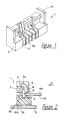
- electrical connector 1 of the preferred embodiment is one for substrate 4 having contact pads (not shown) on both surfaces along the edge.
- Connector 1 comprises a plurality of contacts 3 retained at a constant pitch in a housing 2 made from a suitable plastic material.
- a pair of symmetrical connectors 1 are disposed on a printed circuit board 5 in opposite relationship to each other as shown in Figures 3A-3C.
- the substrate 4 is clipped between a pair of connectors 1 with contacts 3 contacting both upper and bottom surfaces of the substrate 4.
- the contact 3 has at one end thereof, a first contact section 6 in contact with the upper surface 4a of the substrate 4 and at another end thereof a second contact section 7 in contact with the bottom surface 4b.
- the contact 3 is an integral generally C-shaped member comprising an upper contact leaf 3a including the first contact section 6 and a lower contact leaf 3b including the second contact section 7.
- the two contact sections 6 and 7 are integrally coupled to each other by way of a resilient section 9 and a tine section 10.
- the substrate 4 is supported between the contact sections 6, 7 intercoupled by a common tine section 10.
- a stopper section 8 is formed at a free end of the first contact section 6 of the upper contact leaf 3a. Also, a resilient section 9 is formed above the first contact section 6.
- the resilient section 9 integral with the stopper section 8 is resiliently movable toward inside of the housing. When a force is applied toward inside of the housing (as represented by an arrow E), the resilient section 9 is resiliently deformed. Accordingly, both of the first contact section 6 and the stopper section 8 resiliently move toward inside of the housing, thereby providing a space to insert the substrate 4 between the contact sections 6 and 7.
- the lower contact leaf 3b has the tine section 10 to interconnect the two contact sections 6 and 7.
- the tine section 10 is formed by externally exposing the contact leaf 3b from the bottom of the housing 2.
- the connector 1 is mounted on the printed circuit board 5 by soldering at the tine section 10.
- a pair of connectors 1a, 1b each having a plurality of such contacts 3 are mounted on the circuit board 5 in opposite relation to each other. Illustrated in Figures 3A through 3C are the steps of installation of the substrate 4 between such connectors 1a, 1b.
- One edge 4c of the substrate 4 is inserted between the contact sections 6, 7 of one connector 1a and a force is simultaneously applied in the direction of insertion of the substrate 4 to push the stopper section 8 by one edge 4c as illustrated by arrow A. Accordingly, the resilient section 9 is resiliently deformed, thereby resiliently moving the first contact section 6 from its contacting position to the substrate installation position.
- One edge 4c is, then, inserted between the contact sections 6, 7 and the other edge 4d is permitted to move downwardly near the contact sections 6, 7 of the other connector 1b (in the direction as represented by an arrow B), thereby placing the substrate 4 between the connectors 1a, 1b as illustrated in Figure 3B.
- the substrate 4 Since the substrate 4 had been pushed toward connector 1a, the substrate 4 is biased to the connector 1a, thereby remaining at a non- contacting position with the contact sections 6, 7 of the other connector 1b.
- the recovering force of the resilient section 9 pushes back in the direction as represented by an arrow C and the substrate 4, having one edge 4c abutting against the stopper 8, moves to the proper position for making contact with the contact sections 6, 7 of the both connectors 1a, 1b as illustrated in Figure 3c.
- the edge 4d of the other connector 1b abuts against the stopper 8 which applies a pressure to resiliently push the substrate 4 in the direction as represented by an arrow D.
- the substrate 4 is, then, latched at a proper position.
- beads 20 are formed on the bottom surfaces of the tine sections 10 along the longitudinal direction thereof and extending toward the printed circuit board 5 to insure soldering of the tine sections 10 on the printed circuit board 5.
- the bottom surfaces of the beads 20 abuts against the printed circuit board 5 when mounted thereon, thereby avoiding the side edges of the beads of the tine sections 10 to abut against the printed circuit board 5. Gaps created by such particular construction allows solder 21 to flow along the side edges in order to improve strength of the soldering between the printed circuit board 5 and the tine section 10.
- the substrate 4 and the contacts 3 are not soldered in the present embodiment, rather the substrate 4 is installed onto a proper position where the contact sections 6, 7 of the contact 3 are in contact with the upper and bottom surfaces of the substrate 4. This allows the substrate 4 to be easily removed from the connector after installation for convenience of troubleshooting of the substrate or other purposes.
- positioning of the contacts 3 in isolation walls 2b within the housing 2 maintains the pitch of the contacts 3 during mounting, thereby enabling the substrate 4 to be installed between the contacts 3 supported at predetermined pitch. Additionally, positioning the substrate 4 between end walls 2a of the housing 2 effectively aligns the conductive patterns on the substrate 4 with the contacts 3.
- Resiliently movable construction of the contact sections 6 by virtue of the resilient sections 9 absorbs certain differences in the distance between the two connectors 1a, 1b and in the thickness of the substrate (0.40 through 0.65 mm), thereby providing further stable support of the substrate 4.
- the connector occupies minimum area.
- an electrical connector for electrically engaging opposite edges of a substrate.
- the connector includes C-shaped contacts retained in a housing at a constant pitch.
- the contacts include resilient sections for engaging the substrate with one section having a stopper section which abuts the edge of the substrate whereby the section is resiliently moved in as the substrate is inserted and then returns to properly center the substrate.
Landscapes
- Engineering & Computer Science (AREA)
- Microelectronics & Electronic Packaging (AREA)
- Coupling Device And Connection With Printed Circuit (AREA)
Applications Claiming Priority (2)
| Application Number | Priority Date | Filing Date | Title |
|---|---|---|---|
| JP1219010A JPH0381980A (ja) | 1989-08-25 | 1989-08-25 | 電気コネクタ |
| JP219010/89 | 1989-08-25 |
Publications (1)
| Publication Number | Publication Date |
|---|---|
| EP0420407A1 true EP0420407A1 (de) | 1991-04-03 |
Family
ID=16728846
Family Applications (1)
| Application Number | Title | Priority Date | Filing Date |
|---|---|---|---|
| EP90308942A Withdrawn EP0420407A1 (de) | 1989-08-25 | 1990-08-14 | Elektrischer Steckverbinder |
Country Status (2)
| Country | Link |
|---|---|
| EP (1) | EP0420407A1 (de) |
| JP (1) | JPH0381980A (de) |
Cited By (2)
| Publication number | Priority date | Publication date | Assignee | Title |
|---|---|---|---|---|
| EP0570138A3 (de) * | 1992-05-12 | 1994-10-19 | Ibm | Tragbares Plattenspeichergerät. |
| EP0827240A3 (de) * | 1996-08-27 | 1998-09-23 | AMPHENOL-TUCHEL ELECTRONICS GmbH | Kontaktträger |
Families Citing this family (1)
| Publication number | Priority date | Publication date | Assignee | Title |
|---|---|---|---|---|
| US5292265A (en) * | 1993-03-02 | 1994-03-08 | Molex Incorporated | Edge mounted circuit board electrical connector |
Citations (4)
| Publication number | Priority date | Publication date | Assignee | Title |
|---|---|---|---|---|
| US3689684A (en) * | 1971-02-05 | 1972-09-05 | Du Pont | Lead frame connector and electronic packages containing same |
| DE2413989A1 (de) * | 1973-03-23 | 1974-09-26 | Electrovac | Kontaktleiste |
| DE2930506A1 (de) * | 1979-07-27 | 1981-03-26 | Licentia Patent-Verwaltungs-Gmbh, 60596 Frankfurt | Kontaktanordnung |
| DE8622143U1 (de) * | 1986-08-19 | 1986-10-23 | Du Pont de Nemours (Nederland) B.V., Dordrecht | Reihe von Randverbindungsklammern oder einzelne Randverbindungsklammer |
-
1989
- 1989-08-25 JP JP1219010A patent/JPH0381980A/ja active Pending
-
1990
- 1990-08-14 EP EP90308942A patent/EP0420407A1/de not_active Withdrawn
Patent Citations (4)
| Publication number | Priority date | Publication date | Assignee | Title |
|---|---|---|---|---|
| US3689684A (en) * | 1971-02-05 | 1972-09-05 | Du Pont | Lead frame connector and electronic packages containing same |
| DE2413989A1 (de) * | 1973-03-23 | 1974-09-26 | Electrovac | Kontaktleiste |
| DE2930506A1 (de) * | 1979-07-27 | 1981-03-26 | Licentia Patent-Verwaltungs-Gmbh, 60596 Frankfurt | Kontaktanordnung |
| DE8622143U1 (de) * | 1986-08-19 | 1986-10-23 | Du Pont de Nemours (Nederland) B.V., Dordrecht | Reihe von Randverbindungsklammern oder einzelne Randverbindungsklammer |
Non-Patent Citations (1)
| Title |
|---|
| IBM TECHNICAL DISCLOSURE BULLETIN vol. 28, no. 10, March 1986, pages 4360,4361, New York, US; "Surface Mount Substrate Lead" * |
Cited By (3)
| Publication number | Priority date | Publication date | Assignee | Title |
|---|---|---|---|---|
| EP0570138A3 (de) * | 1992-05-12 | 1994-10-19 | Ibm | Tragbares Plattenspeichergerät. |
| EP0827240A3 (de) * | 1996-08-27 | 1998-09-23 | AMPHENOL-TUCHEL ELECTRONICS GmbH | Kontaktträger |
| US6000969A (en) * | 1996-08-27 | 1999-12-14 | Amphenol-Tuchel Electronic Gmbh | Contact carrier including an insulating body and contacts positioned therein |
Also Published As
| Publication number | Publication date |
|---|---|
| JPH0381980A (ja) | 1991-04-08 |
Similar Documents
| Publication | Publication Date | Title |
|---|---|---|
| US5137456A (en) | High density, separable connector and contact for use therein | |
| US4645279A (en) | Chip carrier socket having improved contact terminals | |
| JP3746106B2 (ja) | 基板用電気コネクタ | |
| US4550959A (en) | Surface mountable coefficient of expansion matching connector | |
| US6315620B1 (en) | System, method, and device for a pre-loaded straddle mounted connector assembly | |
| US4891019A (en) | Electrical connector for interconnecting a printed circuit board to a ribbon cable | |
| KR0141902B1 (ko) | 모서리 장착식 회로 기판용 전기 커넥터 | |
| EP0838101B1 (de) | Elektrische verbinder | |
| JPH08124637A (ja) | 表面実装型電気コネクタ | |
| JPH10284194A (ja) | 一体化されたpcbアセンブリを有する表面実装コネクタ | |
| US5558540A (en) | Multi-connector assembly | |
| KR950702752A (ko) | 배면 납작형 카드 커넥터(Flat Back Card Connector) | |
| US20010004555A1 (en) | Plug connector | |
| EP0407531A1 (de) | Chipträger-sockel niedriger bauhöhe. | |
| JP3044377U (ja) | プリント回路基板取付型電気コネクタ | |
| JP2000067966A (ja) | 電気コネクタ | |
| US6834791B2 (en) | Solder-bearing components and method of retaining a solder mass therein | |
| EP0420407A1 (de) | Elektrischer Steckverbinder | |
| US6729916B2 (en) | Board-to-board electrical connector and method for manufacturing same | |
| KR101029668B1 (ko) | 표면장착 헤더 조립체 | |
| US4401352A (en) | Connector system for connecting a ceramic substrate to a printed circuit board | |
| JPH0617164U (ja) | 平板状接続部材のコネクタ装置 | |
| EP0578737B1 (de) | Kontaktvorrichtung für ein elektrisches oder elektronisches bauteil | |
| KR0118721Y1 (ko) | 전기접속용 커넥터 | |
| JP3062921B2 (ja) | コネクタ |
Legal Events
| Date | Code | Title | Description |
|---|---|---|---|
| PUAI | Public reference made under article 153(3) epc to a published international application that has entered the european phase |
Free format text: ORIGINAL CODE: 0009012 |
|
| STAA | Information on the status of an ep patent application or granted ep patent |
Free format text: STATUS: THE APPLICATION HAS BEEN WITHDRAWN |
|
| 17P | Request for examination filed |
Effective date: 19901227 |
|
| AK | Designated contracting states |
Kind code of ref document: A1 Designated state(s): DE FR GB IT |
|
| 18W | Application withdrawn |
Withdrawal date: 19910315 |