EP0421315A2 - Verfahren zum selektiven Entfernen einer Isolationsschicht - Google Patents
Verfahren zum selektiven Entfernen einer Isolationsschicht Download PDFInfo
- Publication number
- EP0421315A2 EP0421315A2 EP90118784A EP90118784A EP0421315A2 EP 0421315 A2 EP0421315 A2 EP 0421315A2 EP 90118784 A EP90118784 A EP 90118784A EP 90118784 A EP90118784 A EP 90118784A EP 0421315 A2 EP0421315 A2 EP 0421315A2
- Authority
- EP
- European Patent Office
- Prior art keywords
- film
- insulating film
- temperature
- vapor
- approximately
- Prior art date
- Legal status (The legal status is an assumption and is not a legal conclusion. Google has not performed a legal analysis and makes no representation as to the accuracy of the status listed.)
- Withdrawn
Links
Images




Classifications
-
- H—ELECTRICITY
- H10—SEMICONDUCTOR DEVICES; ELECTRIC SOLID-STATE DEVICES NOT OTHERWISE PROVIDED FOR
- H10P—GENERIC PROCESSES OR APPARATUS FOR THE MANUFACTURE OR TREATMENT OF DEVICES COVERED BY CLASS H10
- H10P50/00—Etching of wafers, substrates or parts of devices
- H10P50/20—Dry etching; Plasma etching; Reactive-ion etching
- H10P50/28—Dry etching; Plasma etching; Reactive-ion etching of insulating materials
- H10P50/282—Dry etching; Plasma etching; Reactive-ion etching of insulating materials of inorganic materials
- H10P50/283—Dry etching; Plasma etching; Reactive-ion etching of insulating materials of inorganic materials by chemical means
-
- H—ELECTRICITY
- H10—SEMICONDUCTOR DEVICES; ELECTRIC SOLID-STATE DEVICES NOT OTHERWISE PROVIDED FOR
- H10P—GENERIC PROCESSES OR APPARATUS FOR THE MANUFACTURE OR TREATMENT OF DEVICES COVERED BY CLASS H10
- H10P70/00—Cleaning of wafers, substrates or parts of devices
- H10P70/20—Cleaning during device manufacture
- H10P70/23—Cleaning during device manufacture during, before or after processing of insulating materials
Definitions
- the present invention relates to methods for removing insulating films such as native silicon oxide films formed on a surface of a silicon wafer, a surface of a polysilicon film, a surface of an amorphous silicon film and the like (those surfaces being called hereinafter "silicon layer surfaces”) and furthermore the present invention relates to a method for selectively removing insulating films such as a thermal silicon dioxide film (th-SiO 2 ), a silicon nitride (SiN 2 ) film, a phosphosilicate glass (PSG) film, a boro-phosphosilicate glass (BPSG) film, or an arsenosilicate glass (AsSG) film forming a semiconductor device, in addition to the native silicon oxide film.
- a thermal silicon dioxide film th-SiO 2
- SiN 2 silicon nitride
- PSG phosphosilicate glass
- BPSG boro-phosphosilicate glass
- AsSG arsenosilicate glass
- the above PSG film is a binary oxide of P 2 O 2 and generally is deposited in the SiH 4 + O 2 + PH 3 gas system by CVD (Chemical Vapor Deposition) method, while BPSG film is a ternary oxide of B 2 O 3 - P 2 O 5 - SiO 2 and generally deposited in the SiH 4 + O 2 + PH 3 + B 2 H 6 gas system by the CVD method.
- contamination sometimes occurs and exerts adverse effect on the operation characteristics of the device.
- One of the contaminants is a native silicon oxide film formed on a silicon layer surface.
- a native oxide film is easily formed to a thickness of 10 to 20 ⁇ on a surface of a silicon layer by merely exposing the same to the atmosphere.
- a native oxide film is also formed secondarily in a cleaning or an etching step in a semiconductor device manufacturing process.
- a normal electrode function cannot be obtained if a native oxide film remains on the surface of a silicon wafer where electrodes such as a source, a drain and the like are to be formed.
- a native oxide film should be completely removed from a silicon layer surface in order to suppress contact resistance. Also in the case of effecting epitaxial growth of silicon, it is necessary to remove in advance a native oxide film from the silicon layer surface.
- the native silicon oxide film formed on the silicon layer surface should be necessarily removed in a semiconductor device manufacturing process, particularly prior to forming a film by chemical vapor deposition (CVD), sputtering or the like.
- CVD chemical vapor deposition
- sputtering or the like.
- a surface of a silicon wafer is subjected to various film forming steps.
- silicon insulating films such as a silicon oxide film, a silicon nitride film, a PSG film, a BPSG film and an AsSG film are formed by thermal oxidation, CVD and other methods on the silicon wafer.
- the native oxide film but also the silicon insulating film formed especially on the wafer is removed from the water surface.
- wafers not only on a silicon wafer but also on a semiconductor wafer such as a gallium arsenide (those wafers being generally called hereinafter "wafers"), there may be formed any film on a polysilicon film or an amorphous silicon film previously formed on the wafer. In this case also, it is necessary to remove in advance the native silicon oxide film on the surface of the polysilicon film or amorphous silicon film.
- the HF gas concentration in nitrogen (N 2 ) gas for dilution is controlled under a condition of a considerably low concentration of H 2 O component in the atmosphere. This makes it possible to selectively remove only the native oxide film from the silicon wafer surface.
- an object of the present invention is to selectively remove a desired insulating film in a relatively simple and easy process.
- Another object of the present invention is to provide a method of selectively removing a first insulating film with respect to a second insulating film without considerably decreasing water in the atmosphere.
- a further object of the present invention is to enable selective removal of a desired insulating film by HF gas without requiring accurate dilution of the HF gas.
- An additional object of the present invention is to provide a method of selectively removing a desired insulating film by using mixture of HF gas and water vapor without depending on a mixing ratio of HF and H 2 O.
- a method according to the present invention includes the steps of preparing vapor containing hydrogen fluoride and water, relatively keeping a temperature of said vapor higher than a temperature of the wafer surface by a prescribed range, the prescribed range being determined by the first insulating film and the second insulating film, and applying the vapor to said wafer surface, whereby the first insulating film is selectively etched and removed with respect to the second insulating film by the hydrogen fluoride.
- the removal of, for example, the native silicon oxide film proceeds in the following manner.
- hydrofluoric acid vapor is supplied to the silicon layer surface, the hydrofluoric acid vapor is adsorbed on the silicon layer surface.
- the native silicon oxide film formed on the silicon layer surface is etched by a reaction represented by the following chemical formula, in the presence of H 2 O. SiO 2 + 6HF ⁇ H 2 SiF 6 + 2H 2 O
- fluorosilisic acid H 2 SiF 6
- H 2 SiF 6 is present with a high concentration in a liquid film covering the surface of the native silicon oxide film.
- H 2 SiF 6 is divided into SiF 4 and HF gas and soon evaporated (H 2 SiF 4 ⁇ SiF 4 ⁇ + 2HF ⁇ ) and removed from the silicon layer surface.
- the temperature of the silicon layer surface is kept higher than the temperature of the hydrofluoric acid vapor by from 10°C to 50°C, preferably from 12°C to 40°C.
- the hydrofluoric acid vapor is supplied to the silicon layer surface, adsorption of the hydrofluoric acid vapor onto the silicon layer surface is suppressed.
- the invention it is possible to selectively remove not only the native silicon oxide film with respect to the thermal silicon dioxide, but also a first insulating film such as PSG film with respect to a second insulating film such as the thermal silicon dioxide film.
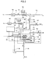
- an apparatus for applying a method of removing a native silicon oxide film on a silicon layer surface includes: an outer container 10 for isolating the inside from the outside airtightly; an inner tube 12 penetrating the outer container 10 and having an inlet 14 and an outlet 16 for gas and vapor; and a gas supply unit 38 for supplying N 2 gas, HF gas and H 2 O vapor to the inlet 14 of the inner tube 12.
- An intermediate portion of the inner tube 12 has an opening within the outer container 10.
- a wafer heating chamber 18 and a vapor heating chamber 20 are provided opposite to each other.
- the wafer heating chamber 18 has an inlet 22 and an outlet 24 of heated air.
- the vapor heating chamber 20 has an inlet 26 and an outlet 28 of heated air.
- the vapor heating chamber 20 is closed airtightly.
- An ultraviolet radiation lamp 30 and an end point sensor 32 are provided inside the vapor heating chamber 20.
- a silicon wafer W to be cleaned is placed with the surface (the upper surface in the figure) to be cleaned being directed to the passage in the inner tube 12, in an opening of the wafer heating chamber 18 facing the opening of the inner tube 12.
- the silicon wafer W isolates the inner tube 12 from the wafer heating chamber 18.
- a flow path of gas and vapor is formed by the inner tube 12, the silicon wafer W and a wall of the vapor heating chamber 20 opposite to the silicon wafer W.
- the wafer heating chamber 18 is provided with a temperature controller 34 for maintaining the surface of the silicon wafer W at a desired temperature.
- the vapor heating chamber 20 is provided with a temperature controller 36 for maintaining the vapor in the inner tube 12 at a prescribed level.
- the gas supply unit 38 includes a hydrofluoric acid tank 102 for storing hydrofluoric acid to be used for treatment.
- a hydrofluoric acid tank 102 for storing hydrofluoric acid to be used for treatment.
- To the hydrofluoric acid tank 102 is connected the flow lines 104 and 106.
- An opening communicating with a flow line 116 for drain is provided in the bottom surface of the hydrofluoric acid tank 102.
- a pump 128 is connected to the hydrofluoric acid tank 102 through flow lines 130 and 132. The pump 128 is used to agitate the hydrofluoric acid in the hydrofluoric acid tank 102.
- a temperature sensor 152, a heater 126 and a flow line 120 are provided in the hydrofluoric acid tank 102.
- the temperature sensor 152, the heater 126 and the flow line 120 are connected to a temperature controller 124.
- the flow line 120 is used for passage of cold water and it has a helical form in the hydrofluoric acid tank 102 and is further connected to the flow line 116 through a flow line 118.
- the hydrofluoric acid tank 102 further includes a level controller 122.
- the level controller 122 is used to regulate a level of hydrofluoric acid in the hydrofluoric acid tank 102.
- the hydrofluoric acid tank 102 further includes a pressure gauge 158.
- the pressure gauge 158 is used to control a valve 142 provided in the flow line 106, and a valve 146 provided in the flow line 110 for drain from the hydrofluoric acid tank 102, thereby controlling the pressure in the hydrofluoric tank 102.
- the temperature controller 124 is responsive to a temperature of hydrofluoric acid detected by the temperature sensor 152 to regulate the temperature of the hydrofluoric acid in the tank 102 by controlling the valve 150 of the flow line 120 and the heater 126.
- the flow line 106 includes a mass flow controller 140, a heater 156, and a temperature controller 136 for controlling the heater 156.
- N 2 gas is supplied from a gas source, not shown, to the flow line 106.
- the gas supply unit 38 further includes a flow line 112 through which the N 2 gas from the source not shown passes.
- the flow line 108 from the tank 102 is joined with the flow line 112, thereby forming a flow line 114 communicating with the inlet 14.
- the flow line 112 includes a mass flow controller 138, a valve 141, a heater 154, and a temperature controller 134 for controlling the heater 154.
- the flow line 108 includes a valve 144. By regulation of the valves 141, 144, N 2 gas supplied by the flow line 112 or hydrofluoric acid vapor supplied from the tank 102 is selectively supplied to the inlet 14 of the inner tube 12.
- the end point sensor 32 is used to detect an end point of treatment. Normally, the end point sensor 32 includes a light projecting fiber and a light receiving fiber, not shown.
- the light projecting fiber is used to apply a coherent beam to the surface of the silicon wafer W.
- the beam is reflected on the upper surface of a film on the silicon wafer W and the lower surface of the film.
- the reflected beams are received by the light receiving fiber.
- the two reflected beams interfere with each other due to the optical path difference thereof. Since the optical path difference is equal to twice the thickness of the film, it is possible to know a proceeding stage of the treatment by examining the intensity of the reflected becomes. Normally, the reflected becomes are converted to voltage by a photodiode or the like and a change in the level is examined whereby the end point of the treatment is detected.
- a silicon wafer W is fed into the outer container 10 and it is set in a prescribed position as shown in Fig. 1.
- the feeding of the wafer W is effected by a mechanical conveyer or the like capable of holding the wafer W by vacuum contact or the like.
- the ultraviolet radiation lamp 30 emits ultraviolet onto the surface of the silicon wafer W. Oxygen excited by the ultraviolet decomposes and removes impurity organic materials adhering to the surface of the silicon wafer W.
- N 2 gas is introduced through the inlet 14 into the inner tube 12 so that the inner tube 12 is purged by N 2 gas.
- the introduction of N 2 gas into the inner tube 12 is effected by opening the valve 141 and closing the valve 144 shown in Fig. 2.
- N 2 gas is mentioned by way of example and any gas may be used insofar as it is inert to the silicon layer surface to be treated and the inner walls of the chamber.
- the temperature controller 34 measures the surface temperature of the wafer W and regulates the temperature of the heated air supplied to the wafer heating chamber 18 through the inlet 22 based on the measured value.
- hydrofluoric acid (HF/H 2 O) vapor is introduced into the inner tube 12 through the inlet 14 in place of N 2 gas.
- the temperature controller 36 measures the temperature of the vapor supplied to the vapor heating chamber 20 through the inlet 26.
- the temperature controller 36 regulates the temperature of heated air based on the measured value.
- the hydrofluoric acid vapor introduced into the inner tube 12 has the temperature maintained at a prescribed level by the temperature controller 36.
- the hydrofluoric acid vapor is introduced into the inner tube 12.
- the surface of the silicon wafer W is exposed to the hydrofluoric acid vapor.
- the native oxide film formed on the silicon wafer W is etched and removed from the surface of the silicon wafer W.
- the surface temperature of the silicon wafer W is maintained higher than the temperature of the hydrofluoric acid vapor by 20°C or more.
- condensation of the hydrofluoric acid vapor onto the surface of the silicon wafer W is suppressed.
- Etching of the thermal silicon dioxide film, CVD silicon dioxide film and the like formed on the silicon wafer W hardly proceeds.
- the flow lines are switched and N 2 gas is introduced again into the inner tube 12.
- the inner tube 12 is purged by N 2 gas.
- the completion of the removal of the native oxide film is detected by monitoring an output of the end point sensor 32 as is described previously.
- the vapor heating chamber 20 containing the ultraviolet radiation lamp 30 and the end point sensor 32 needs to have a transparent portion facing the inside of the inner tube 12. Therefore, a partition wall of this portion is formed by quartz glass.
- quartz glass is corroded by hydrofluoric acid vapor. In order to prevent the corrosion, it is necessary merely to keep the surface temperature of the partition wall of quartz glass higher than the temperature of hydrofluoric acid vapor by 20°C or more.
- the vapor supplied through the vapor inlet 14 may be mixture of hydrogen fluoride gas and water vapor. Any gas mixture may be employed insofar as it contain hydrogen fluoride and water.
- the apparatus used in those experiments includes: a wafer heating cylinder 40 containing a heater 42 and having an outlet 44 and an opening formed at its top end; and a container 46 containing hydrofluoric acid L and having an outlet 48.
- a wafer W is attached to the opening of the top end of the cylinder 40.
- a detection tip of a temperature sensor 50 is in contact with the surface of the wafer W.
- the top end of the wafer heating cylinder 40 is inserted obliquely in the container 46 and the cylinder 40 is positioned in the container 46 in an airtight manner.
- the draft chamber is a local evacuating chamber used at the time of performing a dangerous chemical experiment or the like.
- An operator outside the draft chamber controls the operation of the apparatus in the draft chamber. For that purpose, an opening for the work is provided in the front surface of the draft chamber. Air in the draft chamber is forced to flow out from an outlet provided in the ceiling of the draft chamber.
- the draft chamber is evacuated, whereby vapor V in the container 46 is discharged through the outlet 48.
- the wafer W was kept inclined in the container 46. Since the wafer W was thus held, the flow of the vapor V in the container 46 was not obstructed. The vapor contacted uniformly the surface of the wafer W. As a result, the whole surface of the wafer W was uniformly treated.
- the draft chamber was maintained at room temperature (22°C).
- the temperatures of hydrofluoric acid L and fluorine vapor V in the container 46 were also maintained at the room temperature.
- the surface temperature of the wafer W was regulated.
- Aqueous solution containing hydrogen fluoride of 50% was used as the hydrofluoric acid L.
- the concentration of the hydrogen fluoride in the hydrofluoric acid vapor V was 1.5wt%.
- the container 46 was under atmospheric pressure.
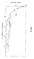
- silicon wafers of 6 inches in diameter (of P type (100)), on each of which a thermal silicon dioxide film of about 5,000 ⁇ in thickness was formed were prepared as specimens. Etching was effected by using the above-mentioned apparatus in both the case where the surface temperature of the wafer W was maintained at the room temperature (22°C) and the case where it was maintained at 65°C. The results were evaluated by measuring and comparing the etching rates.
- Measuring points were common to each wafer. More specifically, the etching rate was measured at 27 points of 5mm intervals along a specified direction of each wafer. An average of the measured values was obtained to express the etching rate.
- An optical interference type film thickness measuring apparatus using a microscopic spectral analyzer was used for measurement of film thickness. The measurement accuracy of this film thickness measuring apparatus was ⁇ 10 ⁇ .
- the results of the measurement are as follows.
- the etching rate of the thermal silicon dioxide film was 1,323 ⁇ /min.
- the thermal silicon dioxide film was hardly etched.
- the etching rate in this case was 0.68 ⁇ /min.
- the results are as follows.
- the thickness of the native oxide film before treatment was 14.7 ⁇ , while the thickness after the treatment was 5.0 ⁇ . Consequently, it can be confirmed that the native oxide film was etched and removed almost entirely from the silicon wafer.
- a measured value by an ellipsometer is assumed to be X 1 .
- a measured value by X-ray electron spectroscopy for chemical analysis (ESCA) is assumed to be X 2 .
- the following relation is established between X 1 and X 2 .
- X 1 - X 2 3.5 to 5.0 ⁇
- the measured value of 5.0 ⁇ by the ellipsometer means that such thickness cannot be detected by measurement by ESCA. Consequently, from the results of the above-mentioned experiments, the wafer is considered to have a surface condition having very little native oxide film.
- the treatment time was selected to be 60 seconds in all cases.
- Measuring points were 27 points at intervals of 5mm along a specified direction of each wafer.
- Evaluation of etching rates was made by an average value of etching rates measured at the respective measuring points.
- Film thicknesses before and after treatment are measured by using the abovementioned optical interference type film thickness measuring apparatus. The measurement accuracy was ⁇ 10 ⁇ .
- the temperatures were set to 23°C, 35°C, 37.5°C, 45°C and 65°C.
- the accuracy of temperature regulation was in the range of about ⁇ 1°C.
- Fig. 4 shows the results of the experiment. Referring to Fig. 4, according to increase of the surface temperature of the silicon wafer, the etching rate of the thermal silicon dioxide film lowers and etching stops at 65°C. A boundary temperature at which etching of the thermal oxide film hardly occurs is about 37.5°C.
- the present invention has been described in connection with one embodiment.
- the above-described embodiment is related with application of the present invention in the case of selectively removing a native silicon oxide film on a silicon wafer.
- the present invention is not limited thereto.
- the native silicon oxide film to be selectively removed may be a native silicon oxide film formed on a surface of a polysilicon film or on a surface of an amorphous silicon film.
- the polysilicon film or amorphous silicon film is not limited to a film formed on a silicon wafer. Such a film may be formed on various semiconductor wafers such as gallium arsenic wafers.
- the wafer is not limited to a silicon wafer. It may be a gallium arsenic wafer or the like.
- the film to be left in selectively removing the native oxide film is not limited to a thermal silicon dioxide film.
- the present invention is also applicable to other silicon oxide film formed, for example, by a CVD method) than the native oxidization, to a silicon nitride film.
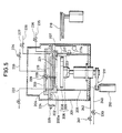
- FIGs. 5 and 6 are schematic views in vertical section illustrating an apparatus for use in practicing the invention, which are detailed in U.S. Pat. Appln. Serial No. 07/518,971, filed on May 4, 1990.
- a housing 201 contains a hydrofluoric acid tank 202 for storing hydrofluoric acid acting as a cleaning solution.
- the hydrofluoric acid tank 202 is closed by a top cover 203, and includes a vapor generating region 204 in an upper space thereof in which vapor is generated from hydrofluoric acid.
- An inner housing 205 is provided inside the housing 201 and immediately under a bottom wall 202a of the hydrofluoric acid tank 202.
- the inner housing 205 accommodates a wafer supporting device 206 for supporting wafer W under treatment.
- a vapor supply section 207 is provided between undersurface of the bottom wall 202a and wafer W for supplying the vapor of hydrofluoric acid.
- the wafer supporting device 206 includes a hot plate 208 rotatable on a vertical axis and containing a heater (not shown), and a support shaft 209 rigidly connected to the hot plate 208.
- the support shaft 209 is operably connected to an electric motor 210 outside the housing 201 through a belt transmission 211.
- the heater contained in the hot plate 208 is controlled by a temperature controller not shown to maintain a surface temperature of the hot plate 208 equal to or above the atmospheric temperature in the vapor supply section 207.
- the inner housing 205 and housing 201 define openings 205a and 201a for allowing passage of the wafer W, respectively.
- Shutters 217 are provided for opening and closing the openings 205a and 201a.
- a flexion arm type wafer transport mechanism 218 disposed outside the opening 201a of the housing 201 is extendible to a position above the hot plate 208 for transporting the wafer W into and out of the inner housing 205. More particularly, the wafer W is delivered as suction-supported by the transport mechanism 218 through the openings 201a and 205a onto the hot plate 208.
- the transport mechanism 218 is retracted outwardly of the housing 201, then the openings 201a dn 205a are closed by shutters 217 and the wafer W is sucked to the hot plate 208.
- the above sequence is reversed. That is, the shutters 217 are opened and the wafer W is carried by the transport mechanism 218 outwardly of the housing 201 through the openings 205a and 201a.
- Each shutter 217 is movable between opening and closing positions by means of a rack (not shown) and a pinion (not shown), the latter being driven by an electric motor 217a.
- the shutters 217 may have any desired construction as long as they enable wafer transport and formation of a gastight space.
- the hydrofluoric acid tank 202 includes hot water piping 219 supported by a holder or holders not shown.
- the bottom wall 202a of the tank 202 defines a hot water passage 221 therein.
- Hot water is circulated through a loop made up of a hot water supply pipe 222 in Fig. 5, the piping 219, passage 221 and a hot water exhaust pipe 223.
- the hot water in circulation heats and evaporates hydrofluoric acid stored in the hydrofluoric acid tank 202.
- the hot water piping 219 and hot water passage 221 constitute heating means for heating and evaporating hydrofluoric acid.
- Reference S1 in Fig. 6 denotes a temperature sensor for measuring temperature of hydrofluoric acid tank 202. The measured temperature is used to control the amount of hot water flowing through the piping 219 and passage 221, thereby maintaining the temperature of hydrofluoric acid below its boiling point.
- the hot water piping 219 may be omitted, with the hot water passage 221 alone used to heat the cleaning solution. Further, oil may be used as a heating medium of hot water.
- the hydrofluoric acid tank 202 includes an overflow passage 224 having an automatic switch valve 224 mounted in an intermediate position thereof. Hydrofluoric acid having the concentration of 39.4% is supplied initially or as replenishment from a storage tank not shown through a supply pipe 226 until it overflows the tank 202. When an overflow occurs, a valve 227 is closed so that an appropriate amount of hydrofluoric acid is stored in the tank 202.
- a temperature controlling device may be provided for the hydrofluoric acid supply pipe 226 since it is desirable to preheat hydrofluoric acid supplied therethrough to a predetermined temperature.
- the construction for supplying the appropriate amount of hydrofluoric acid into the hydrofluoric acid tank 202 may, for example, include a liquid level gauge in the tank 202 for detecting a reduction to a predetermined amount, on the basis of which an appropriate amount of hydrofluoric acid is supplied.
- a vapor supply passage 228 opens to communicate with the vapor generating region 204 at a position above an opening position of the overflow passage 224.
- An end of the vapor supply passage 224 opens through the bottom of the hydrofluoric acid tank 202 into the vapor supply section 207.
- a device 229 is provided for automatically opening and closing the vapor supply passage 228.
- a carrier gas supply pipe 233 is connected to an upper position of the vapor generating region 204 for supplying nitrogen gas N 2 as a carrier gas.
- the carrier gas supply pipe 233 includes a valve 234.
- the carrier gas is used to feed, into the vapor supply passage 228, the hydrofluoric acid vapor collected in the vapor generating region 204 by heating.
- a mixing gas supply pipe 235 is connected to the vapor supply section 207 for supplying nitrogen gas N 2 as a mixing gas.
- the mixing gas supply pipe 235 includes a valve 236.
- each of the carrier gas supply pipe 233 and mixing gas supply pipe 235 has a temperature controlling device for maintaining nitrogen gas flowing therethrough to a predetermined temperature.
- the vapor supply section 207 includes a vapor scattering porous plate 237 defining a vapor space 238 with the bottom wall 202a of the hydrofluoric acid tank 202.
- the vapor supply passage 228 communicates with the vapor space 238 for supplying the hydrofluoric acid vapor to the surface of wafer W on the hot plate 208.
- Hydrofluoric acid in the vapor supply section 207 is maintained at a temperature above its dew point by the heating action of the hot water passage 221 defined in the bottom wall 202a of hydrofluoric acid tank 202 and by the heat from the hot plate 208.
- the hydrofluoric acid tank 202, vapor generating region 204, vapor supply section 207, and vapor supply passage 228 intercommunicating the vapor generating region 204 and vapor supply section 207 are arranged vertically close to one another. These components may, therefore, be heated or temperature-controlled efficiently in a batched manner, to readily prevent condensation of the cleaning vapor flowing therein.
- a first exhaust pipe 240 having a first flow control valve 239 communicates with the interior space of inner housing 205.
- a second exhaust pipe 242 having a second flow control valve 241 communicates with the space defined between inner housing 205 and outer housing 201.
- the first and second exhaust 240 and 242 are connected to respective suction devices not shown.
- the first flow control valve 239 has a larger opening degree than the second flow control valve 241, so that a greater amount of gas is exhausted from inside the inner housing 205 than from space between the two housings 201 and 205.
- This exhaust control arrangement is effective for preventing the hydrofluoric acid vapor exhausted after being supplied to the wafer W from leaking outwardly of the apparatus.
- the exhaust pipe 240 may have a lager diameter than the exhaust pipe 242, with the two pipes 240 and 242 connected to the common suction device or separate suction devices.
- Aqueous solution containing hydrogen fluoride of 39.4% at the temperature of 20°C under the azeotropic condition was used as the hydrofluoric acid L.
- the concentration of the hydrogen fluoride in the hydrofluoric acid vapor V was 0.48 wt% after diluted by N 2 gas.
- the inner housing 205 was under atmospheric pressure.
- the native silicon oxide film was prepared by immersing the wafer in the solution which contains:(a) an aqueous solution of 28 % ammonia NH 4 ; (b) an aqueous solution of 30 % hydrogen peroxide H 2 O 2 ; and (c) water H 2 O.
- the volume ratio of 20 these three components (a) through (c) is 1:1:5.
- the SiNx film was Si 3 N 4 .
- Each of these wafers was subjected to the etching treatment as the temperature thereof was gradually increased from 22°C with the temperature of the hydrofluoric acid vapor being maintained at 22°C.
- the etching rate was measured at 29 points with regard to the wafers (a), (b) and (c), while 21 points the wafers (d), (e) and (f).
- the measuring points were at equal intervals of 5mm along a specified direction of the wafers except for the wafer (d), whose measuring points were at intervals in plural concentric lines. Evaluation of the etching rates was made by an average value of the etching rates measured at the respective measuring points.
- the optical interference type film thickness measuring apparatus using a microscopic spectral analyzer was used for the film thickness measurements for the wafers (a), (b), (c) and (e) whereas the ellipsometer for the wafer (a), (b) and (f).
- the relation was studied between the etching rates of the above insulating film and the temperature differences of the hydrofluoric acid vapor from the wafers.
- Figs. 7A and 7B show the results of the above experiments using optical interference type film thickness measuring apparatus while Fig. 8 the results of the above experiments using ellipsometer.
- the abscissa denotes the temperature difference between the hydrofluoric acid vapor and the wafers, while the ordinate the etching rate. From Figs. 7A and 7B, it can be appreciated that each of the etching amount of the thermal silicon dioxide film, PSG film, and BPSG film per unit time changes. There is a general tendency for the etching rates of these films to lower the temperature difference becomes too large. It appears that the etching of the thermal silicon dioxide film does not occur at the temperature difference of about 12°C.
- the PSG film and BPSG film draw similar curves and continue to be etched until the temperature difference of more than 150°C is reached.
- the etching rate largely depends on the quality and type of the insulating film formed on the wafer.
- the minimal etching selectivity of the PSG and BPSG films from the thermal silicon dioxide film falls within the temperature difference range from 2°C to 8°C, while maximal etching selectivity thereof within the temperature difference range from 14°C to 18°C. Consequently, it is possible to selectively remove the PSG and PBSG films with respect to the silicon thermal oxide film at the temperature difference of 12°C and more. Particularly, it is possible to selectively remove the same within the range of the temperature difference from 14°C to 18°C at a rapid speed.
- the removal of the PSG, BPSG doped oxide films proceeds in the following manner.
- hydrofluoric acid vapor is supplied to the silicon layer surface, the hydrofluoric acid vapor is adsorbed on the silicon layer surface.
- the PSG, BPSG, etc. doped films formed on the silicon layer surface are etched by a reaction represented by the following chemical formula, in the presence of H 2 O. SiO 2 (P,B doped) + 6HF ⁇ H 2 SiF 6 + 2H 2 O
- fluorosilisic acid H 2 SiF 6
- H 2 SiF 6 fluorosilisic acid
- H 2 SiF 6 is present with a high concentration in a liquid film covering the surface of the native silicon oxide film.
- H 2 SiF 6 is soon evaporated and removed from the silicon layer surface.
- the temperature of the silicon layer surface is kept higher than the temperature of the hydrofluoric acid vapor by 15°C or more.
- the hydrofluoric acid vapor is supplied to the silicon layer surface, adsorption of the hydrofluoric acid vapor onto the silicon layer surface is suppressed.
- the etching of the thermal silicon dioxide film was considered to stop at the temperature difference of more than about 12°C based on the measurement using the optical interference type film thickness measuring apparatus. As shown in Fig. 8, however, it is appreciated that the etching somewhat proceeds beyond the temperature difference of 12°C and more based on the measurement utilizing the ellipsometer.
- the values of the etching rates of the silicon thermal oxide film are 3 ⁇ /min at the temperature difference 12°C, 1 ⁇ /min at 18°C and more, and 0.8 ⁇ /min at 38°C, respectively.
- the etching rate of the silicon thermal oxide film gradually decreases as the temperature difference increases.
- the silicon nitride SiN x film and native oxide film also exhibit such tendency.
- the etching rate of the SiN x film is greater than that of the native oxide film and silicon thermal oxide film.
- the etching rate of the native oxide film is larger than those of the thermal oxide film. It appears that the curve drawn by the native oxide film is shifted from that by the thermal silicon dioxide film toward the right side (greater temperature side) in Fig. 8.
- the control of the adsorption amount of the hydrofluoric acid vapor on the wafer enables the high removing selectivity below, raising the temperature of the wafer surface from that of the subject vapor.
- the film to be selectively removed are superposed on the film to be left, or horizontally separately formed on the wafer.
- the concentration of the hydrogen fluoride in the hydrofluoric acid vapor can be set within a wide range from 100% (anhydrous hydrogen fluoride gas) to 1% or less (diluted by N 2 gas). Particularly, it is possible to more stably control the selective removal by applying the anhydrous hydrogen fluoride gas or the azeotropic hydrofluoric acid vapor.
- the present invention makes it possible to provide a new method of selectively removing a native oxide film, which can be applied relatively simply and easily.
Landscapes
- Drying Of Semiconductors (AREA)
- Cleaning Or Drying Semiconductors (AREA)
- Formation Of Insulating Films (AREA)
Applications Claiming Priority (2)
| Application Number | Priority Date | Filing Date | Title |
|---|---|---|---|
| JP258174/89 | 1989-10-02 | ||
| JP25817489 | 1989-10-02 |
Publications (2)
| Publication Number | Publication Date |
|---|---|
| EP0421315A2 true EP0421315A2 (de) | 1991-04-10 |
| EP0421315A3 EP0421315A3 (en) | 1991-11-27 |
Family
ID=17316555
Family Applications (1)
| Application Number | Title | Priority Date | Filing Date |
|---|---|---|---|
| EP19900118784 Withdrawn EP0421315A3 (en) | 1989-10-02 | 1990-10-01 | Method for selectively removing an insulating film |
Country Status (3)
| Country | Link |
|---|---|
| US (1) | US5173152A (de) |
| EP (1) | EP0421315A3 (de) |
| KR (1) | KR930005440B1 (de) |
Cited By (6)
| Publication number | Priority date | Publication date | Assignee | Title |
|---|---|---|---|---|
| US5376233A (en) * | 1992-02-10 | 1994-12-27 | Texas Instruments Incorporated | Method for selectively etching oxides |
| EP0601532A3 (de) * | 1992-12-08 | 1995-04-12 | Nippon Electric Co | Einrichtung und Verfahren für die selektive Ätzung mit HF-Dampf. |
| EP0628993A3 (de) * | 1993-06-09 | 1995-04-12 | Texas Instruments Inc | Methode für die selektive Entfernung von harten Masken in der Herstellung von Graten. |
| EP0704884A3 (de) * | 1994-09-28 | 1996-07-17 | Fsi Int | Verfahren zum Ätzen von Siliziumoxid mit hoher Selektivität |
| EP1083592A1 (de) * | 1999-09-10 | 2001-03-14 | Interuniversitair Microelektronica Centrum Vzw | Ätzen von Siliziumnitrid mittels wasserfreiem Halogengas |
| WO2001037329A1 (en) * | 1999-11-15 | 2001-05-25 | Lucent Technologies, Inc. | System and method for removal of material |
Families Citing this family (21)
| Publication number | Priority date | Publication date | Assignee | Title |
|---|---|---|---|---|
| JP2896268B2 (ja) * | 1992-05-22 | 1999-05-31 | 三菱電機株式会社 | 半導体基板の表面処理装置及びその制御方法 |
| US5376593A (en) * | 1992-12-31 | 1994-12-27 | Micron Semiconductor, Inc. | Method for fabricating stacked layer Si3 N4 for low leakage high capacitance films using rapid thermal nitridation |
| US5913149A (en) * | 1992-12-31 | 1999-06-15 | Micron Technology, Inc. | Method for fabricating stacked layer silicon nitride for low leakage and high capacitance |
| US5429704A (en) * | 1993-11-16 | 1995-07-04 | Sony Electronics, Inc. | Etching tool |
| JP2682510B2 (ja) * | 1995-05-09 | 1997-11-26 | 日本電気株式会社 | 半導体装置の製造方法 |
| US5880032A (en) * | 1995-07-31 | 1999-03-09 | Kabushiki Kaisha Toshiba | Method and apparatus for manufacturing a semiconductor device |
| US5817174A (en) * | 1995-12-15 | 1998-10-06 | Kabushiki Kaisha Toshiba | Semiconductor substrate and method of treating semiconductor substrate |
| US5685951A (en) * | 1996-02-15 | 1997-11-11 | Micron Technology, Inc. | Methods and etchants for etching oxides of silicon with low selectivity in a vapor phase system |
| US6153358A (en) | 1996-12-23 | 2000-11-28 | Micorn Technology, Inc. | Polyimide as a mask in vapor hydrogen fluoride etching and method of producing a micropoint |
| JPH11323576A (ja) * | 1998-05-08 | 1999-11-26 | Sumitomo Precision Prod Co Ltd | ウエットエッチング方法 |
| JP3902726B2 (ja) * | 1998-07-23 | 2007-04-11 | マイクロン・テクノロジー・インコーポレーテッド | 未ドープ二酸化ケイ素に対して選択的に高密度プラズマエッチング器でドープ二酸化ケイ素をエッチングする方法 |
| US6352941B1 (en) * | 1998-08-26 | 2002-03-05 | Texas Instruments Incorporated | Controllable oxidation technique for high quality ultrathin gate oxide formation |
| US6740247B1 (en) | 1999-02-05 | 2004-05-25 | Massachusetts Institute Of Technology | HF vapor phase wafer cleaning and oxide etching |
| US6664196B1 (en) | 1999-03-15 | 2003-12-16 | Matsushita Electric Industrial Co., Ltd. | Method of cleaning electronic device and method of fabricating the same |
| US6746615B1 (en) | 2000-09-14 | 2004-06-08 | Fsi International, Inc. | Methods of achieving selective etching |
| JP2007266482A (ja) * | 2006-03-29 | 2007-10-11 | Toshiba Corp | 生産システム及び電子装置の製造方法 |
| US7883745B2 (en) | 2007-07-30 | 2011-02-08 | Micron Technology, Inc. | Chemical vaporizer for material deposition systems and associated methods |
| GB2487716B (en) * | 2011-01-24 | 2015-06-03 | Memsstar Ltd | Vapour Etch of Silicon Dioxide with Improved Selectivity |
| US20130163124A1 (en) * | 2011-12-22 | 2013-06-27 | Hitachi Global Storage Technologies Netherlands B.V. | Magnetic read sensor having flat shield profile |
| CN111261514B (zh) * | 2018-11-30 | 2024-09-24 | 东京毅力科创株式会社 | 基片处理方法 |
| KR102829691B1 (ko) * | 2020-05-18 | 2025-07-04 | 주식회사 엘지화학 | 열가소성 수지 조성물 |
Family Cites Families (11)
| Publication number | Priority date | Publication date | Assignee | Title |
|---|---|---|---|---|
| GB1539700A (en) * | 1976-05-14 | 1979-01-31 | Int Plasma Corp | Process for etching sio2 |
| JPS54125144A (en) * | 1978-03-24 | 1979-09-28 | Toshiba Corp | Treating device using hydrogen fluoride-containing gas |
| JPS553638A (en) * | 1978-06-21 | 1980-01-11 | Chiyou Lsi Gijutsu Kenkyu Kumiai | Dry etcing |
| US4264374A (en) * | 1978-09-25 | 1981-04-28 | International Business Machines Corporation | Cleaning process for p-type silicon surface |
| JPS5755734A (en) * | 1980-09-19 | 1982-04-02 | Tokyo Shibaura Electric Co | Protecting relay device |
| NL8204437A (nl) * | 1982-11-16 | 1984-06-18 | Philips Nv | Werkwijze voor het vervaardigen van een halfgeleiderinrichting met behulp van plasma-etsen. |
| JPS59166675A (ja) * | 1983-03-11 | 1984-09-20 | Fujitsu Ltd | エツチング装置 |
| US4605479A (en) * | 1985-06-24 | 1986-08-12 | Rca Corporation | In-situ cleaned ohmic contacts |
| DE3650127T2 (de) * | 1985-08-28 | 1995-05-24 | Fsi Int Inc | Verfahren und vorrichtung zum entfernen von schichten von substraten. |
| US4749440A (en) * | 1985-08-28 | 1988-06-07 | Fsi Corporation | Gaseous process and apparatus for removing films from substrates |
| US5174855A (en) * | 1989-04-28 | 1992-12-29 | Dainippon Screen Mfg. Co. Ltd. | Surface treating apparatus and method using vapor |
-
1990
- 1990-09-28 KR KR1019900015577A patent/KR930005440B1/ko not_active Expired - Fee Related
- 1990-10-01 EP EP19900118784 patent/EP0421315A3/en not_active Withdrawn
- 1990-10-02 US US07/591,707 patent/US5173152A/en not_active Expired - Lifetime
Cited By (10)
| Publication number | Priority date | Publication date | Assignee | Title |
|---|---|---|---|---|
| US5376233A (en) * | 1992-02-10 | 1994-12-27 | Texas Instruments Incorporated | Method for selectively etching oxides |
| EP0601532A3 (de) * | 1992-12-08 | 1995-04-12 | Nippon Electric Co | Einrichtung und Verfahren für die selektive Ätzung mit HF-Dampf. |
| EP0732733A1 (de) * | 1992-12-08 | 1996-09-18 | Nec Corporation | Verfahren für die selektive Ätzung mit HF-Dampf und Einrichtung dafür |
| EP0734058A1 (de) * | 1992-12-08 | 1996-09-25 | Nec Corporation | Verfahren für die selektive Ätzung mit HF-Dampf und Einrichtung dafür |
| US5658417A (en) * | 1992-12-08 | 1997-08-19 | Nec Corporation | HF vapor selective etching method and apparatus |
| US6024888A (en) * | 1992-12-08 | 2000-02-15 | Nec Corporation | Vapor selective etching method and apparatus |
| EP0628993A3 (de) * | 1993-06-09 | 1995-04-12 | Texas Instruments Inc | Methode für die selektive Entfernung von harten Masken in der Herstellung von Graten. |
| EP0704884A3 (de) * | 1994-09-28 | 1996-07-17 | Fsi Int | Verfahren zum Ätzen von Siliziumoxid mit hoher Selektivität |
| EP1083592A1 (de) * | 1999-09-10 | 2001-03-14 | Interuniversitair Microelektronica Centrum Vzw | Ätzen von Siliziumnitrid mittels wasserfreiem Halogengas |
| WO2001037329A1 (en) * | 1999-11-15 | 2001-05-25 | Lucent Technologies, Inc. | System and method for removal of material |
Also Published As
| Publication number | Publication date |
|---|---|
| KR930005440B1 (ko) | 1993-06-21 |
| KR910008803A (ko) | 1991-05-31 |
| EP0421315A3 (en) | 1991-11-27 |
| US5173152A (en) | 1992-12-22 |
Similar Documents
| Publication | Publication Date | Title |
|---|---|---|
| US5173152A (en) | Method for selectively removing an insulating film | |
| US5879415A (en) | Semiconductor fabricating apparatus, method for controlling oxygen concentration within load-lock chamber and method for generating native oxide | |
| KR100918005B1 (ko) | 반도체 장치의 제조방법 및 기판처리장치 | |
| US7159599B2 (en) | Method and apparatus for processing a wafer | |
| US5693578A (en) | Method of forming thin silicon oxide film with high dielectric breakdown and hot carrier resistance | |
| US5574247A (en) | CVD reactor apparatus | |
| US7585686B2 (en) | Method and apparatus for processing a wafer | |
| KR950013065B1 (ko) | 건식에칭장치, 건식에칭방법 및 거기서 사용하기 위한 무수 플루오르화수소 기체 발생기 | |
| US7604010B2 (en) | Film formation apparatus and method of using the same | |
| US6821566B2 (en) | Method and apparatus for forming insulating film containing silicon oxy-nitride | |
| US5279705A (en) | Gaseous process for selectively removing silicon nitride film | |
| US5433785A (en) | Thermal treatment apparatus, semiconductor device fabrication apparatus, load-lock chamber | |
| KR20010085636A (ko) | 반도체 제조 방법 및 반도체 제조 장치 | |
| US20090130860A1 (en) | Method of manufacturing a semiconductor device and processing apparatus | |
| JPH03204930A (ja) | 絶縁膜の選択的除去方法 | |
| US6617207B1 (en) | Method and system for forming a stacked gate insulating film | |
| EP1069597A1 (de) | Vorrichtung und Verfahren zur Herstellung von Halbleiterbauelementen | |
| US12557581B2 (en) | Etching method and etching apparatus | |
| JP2596489B2 (ja) | 絶縁膜の除去方法 | |
| JPH0661199A (ja) | 気相エッチング方法および装置 | |
| JP2003115516A (ja) | 水分測定用ウェーハ、水分計の較正方法および熱処理炉の状態評価方法 | |
| JP3317247B2 (ja) | 結晶成長装置および半導体素子の製造方法 | |
| Ogawa et al. | Performance of a new vertical LPCVD apparatus | |
| CN100514034C (zh) | 半导体制造装置的保养时期判断方法 |
Legal Events
| Date | Code | Title | Description |
|---|---|---|---|
| PUAI | Public reference made under article 153(3) epc to a published international application that has entered the european phase |
Free format text: ORIGINAL CODE: 0009012 |
|
| AK | Designated contracting states |
Kind code of ref document: A2 Designated state(s): DE FR GB |
|
| PUAL | Search report despatched |
Free format text: ORIGINAL CODE: 0009013 |
|
| AK | Designated contracting states |
Kind code of ref document: A3 Designated state(s): DE FR GB |
|
| 17P | Request for examination filed |
Effective date: 19920430 |
|
| 17Q | First examination report despatched |
Effective date: 19940328 |
|
| STAA | Information on the status of an ep patent application or granted ep patent |
Free format text: STATUS: THE APPLICATION IS DEEMED TO BE WITHDRAWN |
|
| 18D | Application deemed to be withdrawn |
Effective date: 19940809 |