EP0421325A1 - Asynchrones optisches Zeitmultiplex-Kommunikationssystem - Google Patents
Asynchrones optisches Zeitmultiplex-Kommunikationssystem Download PDFInfo
- Publication number
- EP0421325A1 EP0421325A1 EP90118812A EP90118812A EP0421325A1 EP 0421325 A1 EP0421325 A1 EP 0421325A1 EP 90118812 A EP90118812 A EP 90118812A EP 90118812 A EP90118812 A EP 90118812A EP 0421325 A1 EP0421325 A1 EP 0421325A1
- Authority
- EP
- European Patent Office
- Prior art keywords
- optical
- input
- output
- control
- circuit
- Prior art date
- Legal status (The legal status is an assumption and is not a legal conclusion. Google has not performed a legal analysis and makes no representation as to the accuracy of the status listed.)
- Granted
Links
Images








Classifications
-
- H—ELECTRICITY
- H04—ELECTRIC COMMUNICATION TECHNIQUE
- H04J—MULTIPLEX COMMUNICATION
- H04J14/00—Optical multiplex systems
- H04J14/08—Time-division multiplex systems
-
- H—ELECTRICITY
- H04—ELECTRIC COMMUNICATION TECHNIQUE
- H04Q—SELECTING
- H04Q11/00—Selecting arrangements for multiplex systems
- H04Q11/0001—Selecting arrangements for multiplex systems using optical switching
Definitions
- the invention relates to a multiservice wide optical time band communication system, operating in asynchronous time mode, making it possible to create integrated optical communication networks in which the communications signals are transmitted and switched optically without intermediate transformations of the transmitted signals.
- ATM Asynchronous Transfer Mode
- STM Synchronous Transfer Mode
- BISDN Broad Band Integrated Service Digital Network
- communicating source and receiver are connected for the duration of their communication by a circuit constituted by one or more time channels made up of a succession of cyclic time multiplexes, generally framed.
- Time switching centers provide the necessary spatial and time switching between the various multiplexes used by the circuit, according to a cyclic mechanism using stored control data, for the duration of the communication, in switch control devices of each center.
- the information to be transmitted is formatted at the source in samples of fixed format, successively transmitted on the time channel or channels assigned to the communication.
- the ATM technique combines, by adapting them, the mechanisms of time transmission and packet transmission: Communicating sources and receivers are connected for the duration of the communication by a virtual circuit to which is assigned a physical route consisting of a succession of time-division multiplex links and switching centers. Time resources are used in statistical mode between various sources to which no specific time channel is assigned on the links. A source or receiver can be involved in a multiplicity of different simultaneous communications with different destinations.
- the information to be transmitted is formatted at source in fixed format cells, each comprising identification and routing information; the cells are transmitted acyclically on untimed time-division multiplex links, depending on the availability of unmarked transmission channels.
- Switching cells is therefore akin to time switching, involving spatial switching and time shift.
- the multiplexing mode is statistical, the time shift resources are themselves used statistically and therefore managed as queues. Switching a cell requires prior analysis of the identification and routing information it contains.
- New communication techniques based on optical spectral multiplexing are also known: optical sources and receivers are connected to a passive propagation medium realizing the equal distribution between the receivers of the energy produced by each transmitter.
- the transmitters and the receivers are tunable on a multiplicity of optical frequencies which constitute each one a transmission channel allowing to flow a direction of a communication.
- Three main functional modes are possible: each source is permanently calibrated on an allocated frequency, the communication is established by agreement of the communicating receiver on the said frequency; - each receiver is permanently tuned to an allocated frequency, communication is established by agreement of the communicating transmitter on said frequency; - the frequency is assigned to a communication at the time of its establishment, communicating transmitter and receiver are tuned to said frequency.
- optical frequencies used as a communication medium are, in the best of cases, used for the duration of the communication.
- a multiservice operation which can establish from a single terminal several communications having different destinations, is only possible if the terminals are each equipped with a multiplicity of transmission and reception devices. Each established communication mobilizes one or two optical frequencies.
- the N input buffer memories and the N output buffer memories are electronic memories, .
- the first are each electrically connected by an input device to the receiver of an optical input line and by an output device to a laser tunable in wavelength
- the seconds are each electrically connected by an input device to an optoelectronic receiver tuned to a particular optical wavelength, and by an output device to the transmitter of an optical output line
- the N tunable lasers, each connected to an input buffer memory, and the N wavelength-tuned optoelectronic receivers, each connected to an output buffer memory are optically connected to an NxN passive star optical coupler, .
- the transfer of a packet between an input buffer memory, and an output buffer memory is performed by tuning the emission laser, connected to the output of the input buffer memory, on the tuning wavelength of the optoelectronic receiver connected to the input of the buffer memory recipient output for the duration of the packet transmission.
- the signals to be transmitted undergo several transformations during switching operations, such as opto-electric and electro-optical conversions, (demodulation and remodulation of optical signals), deserialization and serialization of electric signals
- - the routing of the packets requires to exploit routing information included in the packets themselves and therefore to demodulate the carrier signal
- the optical switching device comprising the transmitters, diffuser and receivers, is confined in a restricted space, -
- the capacity of the switching means is limited by the number of discriminable wavelengths, each wavelength being assigned to a receiver.
- the object of the invention is to provide a broadband multiservice optical communication system, in which the transmission and switching of signals is carried out end to end by the only means of optical techniques without requiring a multiple succession of optoelectronic conversions and electro-optics, demodulations and modulations of said signals.
- Another object of the invention is to provide a multiservice optical communication system in which a terminal can, by means of the same optical transmitter and / or the same optical receiver, establish a multiplicity of simultaneous communications having destinations or different origins.
- Another object of the invention is to provide a multiservice optical communication system in which the use of wavelengths or optical frequencies is optimized so as to increase the connection capacity in terminals of the system.
- Another object of the invention is a communication system asynchronous temporal optics which operates without requiring an analysis of the transferred information other than that directly permitted by the sole means of optics and electronic optics without demodulation or prior conversion of the optical communication signals.
- Another object of the invention is to provide the spatial and temporal switches of the optical signals carrying the information by optical and optoelectronic means, themselves controlled by optical signals.
- the subject of the invention is an ATM asynchronous optical time communication system, having: a communication central, q terminal reception circuits connected by at most q optical terminal reception links to the communication central, p transmission circuits of terminal each linked by an optical terminal transmission link to the central office, said terminal transmission and terminal reception circuits being distributed in: x remote communication terminals each having a transmission circuit and a reception circuit, y transmission terminals each having a transmission circuit, z reception terminals each having a reception circuit; characterized in that each terminal reception circuit comprises: . at least one optical configuration receiver, tuned to an optical frequency of a first group of optical frequencies of a first set of optical frequencies; .
- each terminal transmission circuit comprises: . a transmission optical transmitter, tunable to any optical frequency of said second group of optical frequencies; . an optical frequency tuning means of said optical transmitter; . and means for time synchronization and time framing of the information to be transmitted;
- the communication center includes: . an optical spectro-temporal switching device; . control means; . and a synchronization signal generator; in that the switching device is optically connected to the optical transmission links and to the optical reception links; in that the control means comprises: .
- At least one configuration transmission circuit having an optical configuration transmitter tuned to an optical frequency of said first group of optical frequencies; . at least one signaling transmission circuit having an optical transmission transmitter tunable to any optical frequency of said second group of optical frequencies; . at least one configuration reception circuit and at least one signaling reception circuit, each having at least one configuration optical receiver tuned to an optical frequency of said first group of optical frequencies, and a transmission optical receiver tunable to a frequency any of said second group of optical frequencies; in that said exchange is connected to the switching device by: . a control link; . at least one configuration transmit optical link, each being optically connected to the configuration optical transmitter of a configuration transmit circuit; . at least one optical configuration reception link, each being optically connected to the optical configuration and transmission receivers of a configuration reception circuit; .
- At least one optical signaling transmission link each being optically connected to the optical transmitter of a signaling circuit; . and at least one optical signaling reception link, each being optically connected to the optical configuration and transmission receivers of a signaling reception circuit; and in that the synchronization signal generator is connected by a first synchronization link to the switching device and by a second synchronization link to the control means.
- the spectro-temporal switching device comprises: . an optical exploration circuit optically connected to the optical transmission terminals and to the optical signaling transmission links, said optical transmission links each carrying a spectro-time transmission multiplex consisting of channels each carrying a sample information optics; . an optical distributor of control orders; . a control circuit connected on the one hand, optically: .. to the optical exploration circuit by a first optical link carrying a destination spectro-temporal multiplex comprising as many channels as there are transmission links; ..
- optical distributor to the optical distributor by a second optical link carrying a spectro-temporal multiplex of control orders having a number of channels equal to that of said destination multiplex, each channel of the control order multiplex being in time phase with one channel of the same rank of said destination multiplex and routing a control order; .. and to the synchronization generator by the first synchronization link; .. and being connected, on the other hand, to the control means by the control link; . n optical time switches, with controlled propagation, each being optically connected to an output of the optical scanning circuit and to an output of the optical distributor of control orders; . an optical diffuser optically connected at the output of the switches time and optical transmission configuration, and having outputs each optically connected to the input of an optical filter; . s optical filters each optically connected at the output to one of the terminal reception optical connections, signaling reception, configuration reception; . a filter configuration circuit connected at the input to the control link and at the output to a control input for each optical filter.
- the spectro-temporal switching device comprises: . an optical exploration circuit optically connected to the optical transmission terminals and to the optical signaling transmission links, said optical transmission links each carrying a spectro-time transmission multiplex consisting of channels each carrying a sample information optics; . an optical distributor of control orders; .
- a control circuit connected on the one hand, optically: to the optical scanning circuit, by a first optical link carrying a destination spectro-temporal multiplex comprising as many channels as there are transmission links; to the optical distributor, by a second optical link carrying a spectro-temporal multiplex of control orders having a number of channels equal to that of said destination multiplex, each channel of the control order multiplex being a time phase with a transmission channel same rank of said destination multiplex and routing a control order; and to the synchronization generator by the first synchronization link; and connected, on the other hand, to the control means by the control link; . propagation time switching optical means, having: ..
- n input circuits each optically connected to an output of the optical scanning circuit and to an output of the optical distributor of control orders; .. and an output device optically connected as an input to input circuits; . an optical diffuser optically connected at the output of the output device, and to the optical configuration transmission links, and having outputs optically connected each at the input of an optical filter; . s optical filters each optically connected at the output to one of the optical connections receiving terminal, signaling reception, configuration reception; . a filter configuration circuit, connected at the input to the control link and at the output to a control input for each optical filter.
- the destination multiplex is constituted by sampling the channels occurring at the same instant at the input of the exploration circuit on each of the transmission links; . each channel of the control order multiplex having the same rank as a transmission link carries a control order consisting of an optical signal at an optical frequency of a second set of optical frequencies of which each optical frequency is characteristic of a propagation delay in real time which must undergo, in a time switch, the message conveyed by the channel of said transmission link, said optical frequency being determined by the control circuit; and the optical distributor delivers to each time switch, corresponding to the rank of a channel of the control order multiplex, the control order, conveyed by said channel of the control order multiplex.
- the communication system implements several multiplexes: - a time-division broadcast raster multiplex, CEM, called configuration multiplex, of which: . the optical carrier frequency of a Fal group serves as a reference for the optical frequency encoding systems of the terminals; . the frame code is used as a time reference for the time synchronization of the terminals; .
- CEM time-division broadcast raster multiplex
- a time-division multiplex reception not framed, CRM, carrying optical samples carried by a frequency of a group Fa2, which serves as a support for the response messages of the terminals in the configuration operations;
- a pair of so-called signaling multiplexes having a spectro-temporal transmission multiplex SEM and a reception multiplex SRM, used for signaling exchanges between the terminals and the central control means;
- a multiplicity of spectro-time transmission multiplex UEM and a multiplicity of time reception multiplex URM which multiplex UEM and URM are communication multiplexes, which multiplex SEM, SRM, UEM and URM carry optical samples each carried by an optical frequency of the group Fa2.
- the communication system implements for the command: - an OLM multiplex, called destination multiplex; - a CLM multiplex, called a multiplex of control orders, which OLM and CLM multiplex are framed time multiplexes having a period equal to the duration of one channel of the communication multiplexes and a number of channels per frame equal to at least the total number UEL and SEL lines connected to the SSTSN spectro-time switching device.
- the optical samples conveyed by the various multiplexes have a duration T and are temporally formed of a central part, containing the transmitted information, framed on either side of non-information carrying parts constituting switching windows.
- the relative durations of the three parts are such that it is not necessary to achieve, before switching, perfect time alignment of the samples with respect to the local clocks of the switching device in order to avoid degrading the information transmitted.
- the information transmitted is either a digital signal or an analog signal: in the first case, the signal is formatted in cells each containing a multiplicity of bytes, in the second case the signal is temporally divided into samples
- Each cell or signal sample is transmitted by an optical sample encoded at the optical frequency characteristic of the destination of the signal which constitutes the switching reference for the switching means of the exchange and which constitutes the selection reference for the reception means. terminals.
- the control circuit CC comprises a multiplicity of elementary generators of order to control the time switches TSU, each responsible for managing the channels of one of the reception reception multiplexes CRM, SRM and URM and for developing the orders for control of the TSU switches for all the optical samples to be routed on these reception transmission multiplexes whatever the origin.
- the number of generators equipped is at least equal to the number of CRM, SRM and URM multiplexes implemented in the system, equal to the number of frequencies f2 of the second group Fa2 of the optical frequencies and at most equal to the number of discriminable optical frequencies in the optical spectrum.
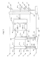
- FIG. 1A shows an exemplary embodiment of a communication system according to the invention, which implements at least one communication center SN to which are connected, on the one hand: .
- p terminal transmission circuits UE UE1 to UEp
- each circuit having an optical transmission transmitter connected to said optical terminal transmission link, an optical frequency tuning means of said optical transmitter, information source means to transmit and time synchronization and time framing means of said information, each circuit being connected by an optical transmission link UEL (UEL1 to UELp); .
- q UR terminal reception circuits (UR1 to URq), each having an optical transmission receiver and at least one configuration optical receiver connected to said optical terminal reception link, an optical frequency tuning means of said optical transmission receiver , a time synchronization means and means for exploiting the information received, each circuit being connected by an optical link for receiving URL (URL1 to URLq); and on the other hand, possibly, one or more broadcasting servers BS, such as for example broadcasting broadcasting audiovisual programs, each by an optical broadcasting link BL.
- broadcasting servers BS such as for example broadcasting broadcasting audiovisual programs
- the said circuits for transmitting the terminal UE and for receiving the terminal UR are distributed in: .. x communication terminals each having a transmission circuit UE and a reception circuit UR, each connected by a link transmission optic UEL and an optical reception link URL, .. y transmission terminals each having a transmission circuit UE, each connected by an optical transmission link UEL, ..z reception terminals each having a circuit UR receiver, each connected by an optical URL receiver link.
- Receiving terminals are generally installed at subscribers or data collection centers.
- the communication terminals are installed with subscribers, in the exchanges interconnected with the SN exchange as well as in the server centers, of which they allow interactive access by the exchange for the management of operation and, possibly by the users, for the management of services. .
- each communication terminal has various other functional means including . a synchronizable generator of clock signals, . an optical frequency reference means, . and a control means supervising the various other functional means.
- the transmission and / or reception terminals grouped together in the same server center and the reception terminals located with subscribers are managed by said other functional means of the communication terminal installed in the server center or at the subscriber.
- optical transmission UEL and URL reception links connecting the same communication terminal are each supported by an optical fiber or use the same optical fiber equipped at its ends with optical duplexers separating the two directions of transmission, associated with means of optical isolation.
- a single optical fiber only supports a single optical transmission link UEL.
- the same optical fiber can support several URL optical links, which fiber is then equipped, at its end remote from the exchange, with an optical diffuser constituted for example by a star optical coupler.
- optical links BL connecting the servers BS of the same server center are each supported by an optical fiber or grouped by means of an optical coupler in the server center on the same optical fiber connecting to the server center.
- the SN central includes the following means: - a SSTSN spectro-temporal switching device having: . two groups of inputs of respective capacity n and m: .. a first group of n inputs I1 to In, of which p are each optically connected to one of the optical links UEL, and of which at least one of the remaining np, such In, is connected to an optical link transmitting signaling SEL; ..
- a group of identical optical outputs including: .. q outputs (O1 to Oq) are, in the general case, each connected to an optical link URL; .. at least one output, such as the On output, is connected to an optical signal receiving signaling SRL; at least one output, such as the Oc output, is connected to an optical reception link of CRL configuration; .
- a synchronization access connected to a synchronization link H1; . a control access connected to a control link CB; - a CPU control means having: . at least one EC configuration transmission circuit comprising a configuration optical transmitter connected to a CEL configuration transmission optical link; . at least one CR configuration reception circuit comprising an optical transmission receiver and at least one optical configuration receiver, connected to a CRL configuration reception link; . at least one signaling transmission circuit SE comprising an optical signaling transmitter connected to an optical signaling transmission link SEL; . at least one signaling reception circuit SR comprising a signaling receiver and at least one configuration receiver, connected to an optical signaling signaling reception SRL; - a CKU synchronization signal generator connected: . to the spectro-temporal switching device SSTSN by the synchronization link H1; . by means of CPU control by a synchronization link H2.
- the CPU control means is connected: to the spectro-temporal switching device SSTSN by said optical configuration and signaling transmission and reception links (CEL, CRL; SEL, SRL) and by a control link CB; . to the synchronization signal generator CKU via the synchronization link H2.
- the latter is connected to only one of the outputs Oi of the spectro-temporal switching device SSTSN.
- Each optical configuration transmitter is tuned to an optical frequency of a first group Fal of optical frequencies, having f1 optical frequencies and belonging to a first set of frequencies Fa which is the set of optical transmission frequencies of the device of the invention , and each optical configuration receiver is tuned, as a function of its rank, to an optical frequency of said first group of optical frequencies.
- Said optical transmission transmitters and optical transmission receivers can be tuned to an optical frequency any of a second group Fa2 of optical frequencies of the set Fa, having f2 frequencies, different from the frequencies of the first group Fa1 of optical frequencies.
- Each broadcasting optical link BL of a broadcasting server BS is connected in the server BS to at least one optical transmitter called the optical broadcasting transmitter, the reception circuits UR optionally comprise one or more optical broadcasting receivers.
- Said optical broadcast transmitters and optical broadcast receivers can be tuned to any optical frequency of a third group Fa3 of optical frequencies of the set Fa, having f3 frequencies, different from the frequencies of the first and second groups Fa1 and Fa2 of frequencies optical.
- each reception circuit UR comprises at least one optical receiver, tunable to any optical frequency of the three groups Fa1, Fa2, Fa3 of optical frequencies constituting the first set Fa of optical frequencies.
- Said first set of optical frequencies Fa, set of optical transmission frequencies of the device of the invention therefore includes the three groups of optical frequencies Fa1, Fa2 and Fa3 having f1, f2 and f3 distinct frequencies respectively.
- frequency is used in the present description for the convenience of the presentation: in fact, it is a narrow spectral band, centered on an optical frequency, discriminable either by means of a filtering device optical, or by means of an optoelectric filtering device known under the name of heterodyne photoreceptor.
- the maximum number, famax, of the optical frequencies of said first set Fa of the optical frequencies is equal to the maximum number, fmax, of the technically discriminable optical frequencies in an optical spectrum by the technical means mentioned above.
- fa ⁇ famax fmax
- Each optical transmitter transmits on the link which is connected to it a time multiplex
- each optical receiver receives by the link to which it is connected at least one time multiplex, which time multiplexes, with the exception of the CEM multiplexes described below, are temporally structured into a series of undifferentiated time channels of duration T, and are not framed.
- each time channel of a series of undifferentiated channels is identifiable by a time reference Ti, relating to the clock of the communication system.
- CEM multiplexes are framed multiplexes with a c-channel frame and a c.T period.
- the first channel of each frame carries an identification code for the start of the frame, as is known in the temporal techniques.
- the other channels are undifferentiated and therefore identical to the channels of the other multiplexes.
- each time channel Ti is transmitted an optical sample of duration T, carrying information to be transmitted.
- the optical carrier frequency of each sample is characteristic of its destination, either functional or physical: the optical frequency encoding of the samples is carried out by the transmission circuit according to their physical or functional destination.
- the information to be transmitted can be either a digital signal or an analog signal: in the first case, the signal is formatted in cells each containing a multiplicity of bytes, for example 36 or 53 bytes, in the second case the signal is temporally cut into samples.
- Each cell or signal sample is transmitted by optical sample encoded at an optical frequency characteristic of the destination of the signal.
- the optical frequency carrying a sample constitutes for the referral means of the central office the referral reference and for the reception means of the terminals the selection reference.
- each optical sample of duration T is temporally formed of a central part, containing the information transmitted, framed on either side of parts, not carrying information, constituting switching windows.
- the relative durations of the three parts are such that it is not necessary to achieve, before switching, perfect time alignment of the samples with respect to the local clocks of the switching device in order to avoid degrading the information transmitted.
- the multiplex When all the optical samples of a multiplex are carried by the same optical frequency, the multiplex is designated below as time multiplex. When the successive optical samples of a multiplex can be carried by different optical frequencies, the multiplex is designated hereinafter as spectro-temporal multiplex.
- Each transmission circuit CE transmits on its CEL link a time multiplex CEM, called configuration transmission multiplex.
- the CEM time multiplexes are, whatever the operating mode of the communication system, framed multiplexes. They are systematically all broadcast by the switching device SSTSN on each of the CRL, SRL and URL links and received by said optical receivers for configuring the reception circuits connected to said links.
- Each CEM time multiplex is carried by one of the f1 optical frequencies of the frequency group Fa1, which optical frequency is characteristic of the rank of the multiplex in the set of CEM multiplexes.
- the optical frequencies of the Fa1 groups are functionally characteristic of the configuration functionality.
- Each transmission circuit SE transmits on its link SEL a spectro-temporal multiplex SEM, known as signaling transmission multiplex
- each transmission circuit UE transmits on its link UEL a spectro-temporal multiplex UEM, known as communication transmission multiplex, which multiplex spectro-temporal SEM and UEM carry a succession of supported optical samples, each according to its destination, by one of the f2 frequencies of the group Fa2 optical frequencies.
- the optical frequencies of the Fa2 groups are functionally characteristic of the communication functionality, including the signaling functionality.
- Each CRL link carries a time multiplex CRM, known as configuration reception multiplex
- each SRL link carries a time multiplex SRM, known as signaling reception multiplex
- each active URL link carries a time multiplex URM, said communication reception multiplex.
- the time multiplexes CRM, SRM and URM are each carried by one of the f2 optical frequencies of the group Fa2 of the optical frequencies, which optical frequency is characteristic, for the switching means, of the rank of the multiplex in the set of multiplexes CRM, SRM and URM, and therefore of a spatial destination in the communication system, which is not necessarily invariant in time as explained in the description of the functioning of the communication system.
- the time multiplexes CRM, SRM and URM are sent optically by the SSTSN device on the CRL, SRL and URL links and received optically by said transmission receivers of the reception circuits connected to said links.
- Each BL link carries at least one multiplex designated below as BCM multiplex; each of the BCM multiplexes is carried by one of the f3 optical frequencies of the Fa3 group, which optical frequency is characteristic of the rank of the BCM multiplex in all of the BCM multiplexes and therefore constitutes, for the central office switching means and the reception circuits terminals, the BCM multiplex selection parameter.
- the optical frequencies of the Fa3 groups are functionally characteristic of the broadcasting functionality.
- the BCM multiplexes are broadcast, optionally selectively, on the URL links by the switching device SSTSN, and received by the said optical distribution receivers of the reception circuits connected to these links.
- an active URL link carries an URM multiplex, all of the CEM multiplex and possibly BCM multiplexes, each CRL link routes a CRM multiplex and the CEM multiplexes, and each SRL link routes an SRM multiplex and the CEM multiplexes.
- the spectro-temporal switching device SSTSN In the central office of the invention, the spectro-temporal switching device SSTSN, - distributes, as a function of their optical carrier frequency Fa2i, each sample of the spectro-temporal multiplex transmission SEM and UEM, to the reception time multiplex CRM, SRM or URM carried by the frequencies Fa2i; - broadcasts on each of the CRL and SRL links the CEM multiplexes and on each of the URL links, in addition to the URM multiplexes concerned, the CEM multiplexes and possibly selectively the BCM multiplexes.
- fmax is the maximum number of technically discriminable optical frequencies in an optical spectrum
- 1B represents the organization of the switching device SSTSN equipping the spectro communication system time of the invention, figure in which: - I1 to In, Ib and Ic are the optical inputs. - O1 to Oq, On and Oc are the optical outputs. - H1 and CB are respectively the synchronization and control links of the SSTSN spectro-time switching device.
- - LS is an optical circuit exploring the input lines carrying the spectro-time emission multiplexes UEM and SEM. LS is optically connected: . by its inputs 210.1 to 210.n at the inputs I1 to In; . by each of its outputs 211.1 to 211.n, at input 501 of an optical time switch TSU; . and by its control input and output 201 and 202 and its output 203, respectively at output 402 and at inputs 403 and 410 of a control circuit CC.
- LS samples the contemporary optical samples of the UEM and SEM multiplexes coming from the inputs I1 to In of SSTSN and present on its inputs 210.1 to 210.n, groups the optical signals obtained in a cyclic spectro-temporal multiplex, called the OLM multiplex which is transmitted on the output 203, and transfers to its outputs 211.1 to 211.n the optical samples received on its inputs.
- - OLM is a multiplex with a useful capacity of n channels each associated with one of the inputs 210.1 to 210.n and therefore with one of the inputs I1 to In of SSTSN.
- I1 has a cycle time equal to the duration T of a channel of the multiplexes of the links connected to the inputs I1 to In.
- the optical signals which it carries are, by their spectral characteristics, similar to the optical samples present on the inputs I1 to In which they come from, and therefore representative of the destinations of said optical samples. They are therefore each supported by an optical frequency of the second group of optical frequencies Fa2.
- - CC is the control circuit of the spectrotemporal switching device. It is optically connected: .. by its accesses 402, 403 and 410 to the line explorer LS as described above; .. by its outputs 404 and 411 and its input 405 respectively at the control inputs 301 and 303 and at the output of order 302 from a CD dispenser; .. by its access 401 to the synchronization link H1; It is also connected, via its access 406, to the control link CB.
- the control circuit CC optically analyzes the signals of the multiplex OLM received on the input 410, generates the control orders of the time switches TSU as a function of the availability of the destination links of the samples present on the inputs I1 to In of the switching device, designated by the spectral characteristics of the signals of the OLM multiplex, and transmits these control orders to the CD distributor by a cyclic spectro-temporal multiplex, called the CLM multiplex, transmitted on the output 411, having the same number n of useful channels and the same period cyclical than the OLM multiplex.
- Each channel of the CLM multiplex is in time phase, to the nearest calculation time, with the same rank channel of the OLM multiplex, and routes the successive control orders of the time switch TSU of the same rank.
- the control orders are developed and transmitted in the form of optical signals each carried by one of the fb optical frequencies of a second set Fb of optical frequencies called the control frequencies of the time switches TSU.
- the second set Fb of optical frequencies is independent of the first set Fa of optical frequencies and can belong to the same spectral domain.
- Each of the fb optical frequencies of the second set Fb of optical frequencies is characteristic of a particular value of the time offset which must undergo, in the SSTSN device, any incident sample of a spectro-time transmission multiplex to be inserted in a free channel. , or an affected channel, of the destination receiving time multiplex, that is to say of a time crossing value by the sample of a time switch TSU.
- each of the fb optical frequencies constitutes both the address of an optical connection point in all the optical connection points equipping the same time switch TSU, and the order of command of said optical connection point.
- - CD is an optical circuit distributing control orders to the time switches TSU1 to TSUn, which control orders are constituted by the optical signals conveyed by the CLM multiplex received on input 303.
- the CD circuit is optically connected by its inputs and control output 301 and 302, and input 303, respectively at ports 404, 405 and 411 of the control circuit CC; and by its outputs 311.1 to 311.n, at the control inputs 502 of the time switches TSU.
- the CD circuit switches to each of the outputs 311.1 to 311.n the control orders conveyed by the CLM multiplex according to their rank in the frame of the multiplex, the succession of the same rank orders of the successive frames of the CLM multiplex constituting the multiplex of TSU switch control orders of the same rank.
- - TSU1 to TSUn are n optical time switches with controlled propagation, each connected: .
- Each switch TSU receives on its input 501 a transmission time multiplex UEM or SEM, and on its control input 502 a control multiplex, each order of which relates to the contemporary optical sample of the transmission multiplex, and, as a function of the control orders received, realizes the temporal rearrangement of the successive optical samples of the input time multiplex.
- - OD is an optical diffuser having: . (m + (nk)) inputs connected to the m inputs of the second group of inputs of SSTSN and of the k outputs of each of the n time switches TSU when these are of the type of FIG. 5A; .or (m + n) inputs when the TSU switches are of the type of FIGS. 5C or 5D; . and s outputs each connected to the input of an optical amplifier filter of a set of s filters WF, set consisting of the filters WF1 to WFq, WFn and WFc of FIG. 1B.
- the OD diffuser performs a spectral multiplexing of all the optical samples presented on its inputs and delivers on each of its outputs a spectral multiplex of all the incident samples.
- One embodiment of such an optical diffuser is described in the French patent application published under the reference 2 625 815: "Optical diffuser of type N by N".
- the WF optical amplifier filters each have an input optically connected to an output of the OD diffuser, an output optically connected to an Oi output of the spectro-temporal switching device SSTSN and a control input connected to the output of a circuit of configuration of the FCC filters, which FCC circuit is connected at the input to the control link CB by which it receives from the control means CPU of the central office the configuration commands for the filters.
- the WF filters are transparent for the frequencies of the first group of optical frequencies Fa1 and can each be tuned to one of the f2 frequencies of the second group of optical frequencies Fa2, which frequency is then characteristic of the destination constituted by optical link reception, URL, CRL or SRL , connected to the filter outlet.
- the WF filters are also tunable on one or more frequencies of the third group Fa3 of the optical frequencies.
- the WF filters are each tuned so: . to be transparent for one or more optical frequency subgroups of the optical frequency groups Fa1 and Fa2, and possibly of the optical frequency group Fa3, each optical frequency subgroup comprising at least one frequency; . and block the propagation of any optical frequency foreign to subgroups of agreement.
- the amplifier filters WF are identically transparent for the three groups of optical frequencies Fa1, Fa2 and Fa3, their filtering function being limited to blocking the propagation of any optical frequency foreign to the three groups.
- the set of WF optical amplifier filters constitutes a spatial distribution device directing on each of the reception links the only multiplexes which concern it. Spatially limiting the distribution of multiplexes, it protects communications.
- the optical samples produced by the sources are modulated between two levels of optical energy, the lowest level of which is such that it enables the circuits of FIG. 4C to operate, identifying the carrier optical frequency.
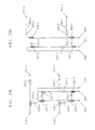
- FIG. 2A the schematic diagram of an embodiment of the exploration circuit of the input lines LS of FIG. 1A, exploration circuit consisting of: - a control device, called “first control device", connected by its input 201 and its output 202 to the control circuit CC; - an optical selector including: . the inputs 210.1 to 210.n are each connected to one of the inputs I1 to In of the switching device SSTSN; . outputs 211.1 to 211.n are each connected to the input of a TSU switch; . the output 203 is connected to the control circuit CC.
- first control device connected by its input 201 and its output 202 to the control circuit CC
- an optical selector including: . the inputs 210.1 to 210.n are each connected to one of the inputs I1 to In of the switching device SSTSN; . outputs 211.1 to 211.n are each connected to the input of a TSU switch; . the output 203 is connected to the control circuit CC.
- Said first control device is formed by an assembly in series of n optical couplers 221.1 to 221.n each having an input and a first and a second output, and of n-1 identical optical delay lines such as 222.1 each having a inlet and outlet, the assembly being such that the first outlet of each coupler, with the exception of the last one, is connected to the input of a delay line whose output is itself connected to the input of the next coupler, the input of the first coupler 221.1 and the first output of the last coupler 221.n being connected respectively to the input 201 and to the output 202 of said first control device, the second outputs of each of the couplers 221.1 to 221.n being connected, possibly via an optical amplifier such as 223.1 to an optical selector control input.
- Said optical selector is formed by an assembly of n optical switches 224.1 to 224.n each having a first and a second input, an output and a control input, and of n optical couplers 226.1 to 226.n each having an input , a first and a second output, and n identical delay lines 227.1 to 227.n, each having an input and an output.
- the optical switches such as 224.1 are put in series by connecting the output of one to the first input of the next, the output of the switch 224.1 being connected to the output 203 of the optical selector; . the second input of each optical switch such as 224.1 is connected to the second output of the coupler of the same rank, such as 226.1, possibly via an optical amplifier, such as 225.1; .
- control switch optical inputs constitute the control inputs of the optical selector and are each connected to the second output of the optical coupler of the same rank as 221.1 of said first control device; . the input of each optical coupler such as 226.1 is connected to the input of the same rank of the n inputs 210.1 to 210.n of the explorer; . the first output of each coupler such as 226.1 is connected to the input of the delay line such as 227.1, the output of which is connected to the output of the same rank as 211.1 of the explorer.
- FIG. 2B represents the block diagram of an embodiment of the distributor CD of the control orders to the time switches TSU.
- Said CD distributor consists of: - a control device, called “second control device", whose input 301 and output 302 are connected to the control circuit CC; - a distribution line whose input 303 is connected to the CC control circuit and whose outputs 311.1 to 311.n are each connected to the control input of a TSU switch.
- Said second control device is formed by an assembly of n couplers with one input and two outputs, 321.1 to 321.n, and by n-1 identical delay lines such as 322.1, assembly identical to that, previously described, of the said first control device of the explorer LS of the input lines.
- Said distribution line is formed of an assembly comprising: . n optical switches 324.1 to 324.n each having an input, a first and a second output and a control input, . n hysteresis optical amplifiers 325.1 to 325.n, . n delay lines 326.1 to 326.n each having a different length characteristic of the rank of the delay line.
- the n optical switches are arranged in series by connecting the first output of one to the input of the next, the input of the switch 324.1 being connected to the input 303 of the distribution line; .. the second outputs of each of the n optical switches are each connected via one of the n optical hysteresis amplifiers to the input of one of the n delay lines; .. the outputs of the n delay lines are each connected to one of the outputs 311.1 to 311.n of the distribution line; the control switch optical inputs, such as 324.1, are each connected to the second output of the coupler of the same rank, such as 321.1, of said second control device, possibly via an amplifier such as 323.1.
- Hysteresis optical amplifiers such as 325.1, are, for example, made up of an optoelectronic amplifier device functioning as a monostable.
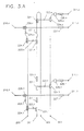
- FIGS. 3A and 3B each describe an embodiment of the line explorer LS and of the order distributor CD in which the said first and second control devices described in FIGS. 2A and 2B are grouped together in a single device command says "third command device”.
- the so-called "third control device” is constituted by assembling in series the n couplers 221.1 to 221.n and the n couplers 321.1 to 321.n already described and n first lines to delay 231.1 to 231.n and n-1 seconds delay lines such as delay line 331.1 according to the following principle: .
- the first output of the coupler 221.i is connected to the input of the delay line 231.i, the output of which is connected to the input of the coupler 321.i, the first output of which is itself connected to the input of the delay line 331.i, the output of the latter being connected to the input of the coupler 221.i + 1.
- the input of the first coupler 221.1 and the first output of the last coupler 321.n being connected respectively to the input 201 and to the output 202 of said third control device.
- the delay created by a couple of delay lines such as 231.1 and 331.1 is equal to the delay created by the delay lines 222.1 or 322.1 of the assemblies of FIGS. 2A or 2B.
- the n-1 delay lines such as 331.1 of said "third control device" would have a zero delay value.
- these n-1 delay lines are not equipped but replaced by a direct connection from the first output of the coupler 321.i to the input of the coupler 221.i + 1, the delay of the delay lines such 231.1 then being equal to the delay created by the delay lines 222.1 or 322.1 of the assemblies of FIGS. 2A or 2B.
- This variant embodiment of the line explorer LS and the order distributor CD is shown in FIG. 3B.
- FIGS. 3A and 3B representing the same functional object, are designated by the reference in FIG. 3.
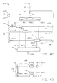
- FIGS. 4A and 4C on the one hand, and the combination of FIGS. 4B and 4C on the other hand, describe the construction of the control circuit CC respectively: . in the case where the line explorer LS and the order distributor CD are produced according to the arrangements described in FIGS. 2A and 2B; . and in the case where they are produced according to the assembly described in FIG. 3 (3A or 3B).
- the control circuit CC in both cases includes a command generation circuit (fig. 4A or 4B) and a generator of control commands (fig. 4C).
- FIGS. 4A and 4B describe the circuit for developing control of the control devices, respectively for the first and second cases defined above, the connection of said control circuit to the external means being as follows: .
- the optical input 401 is optically connected to the synchronization link H1 of the switching device SSTSN, which is itself optically connected to the synchronization signal generator CKU.
- the electrical input 406 is connected to the control link CB, which is itself connected to the central unit's CPU control means. .
- the optical output 402 and optical input 403 (fig. 4A or fig. 4B) are connected respectively to the optical input 201 and the optical output 202 of the control device (fig. 2A or fig. 3).
- the output 404 and the optical input 405 (FIG. 4A) are optically connected respectively to the input 301 and to the output 302 of the control device (FIG. 2B).
- an optical generator 421 of optical pulse of calibrated duration is connected by its input to the input 401 of the circuit and by its output to the input of an optical coupler 422 distributing the optical energy equally. to two outputs, the first of which is directly connected to the first input of a optical switch 423.1 and the second is connected to the input of a delay line 424 whose output is itself connected to the first input of an optical switch 423.2, the switches 423.1 and 423.2 each having two inputs and two outputs and being electrically controllable by the control link CB connected to the input 406.
- the second output of the optical switch 423.1 is connected to the input of a delay line 425.1, the output of which is connected to the output 402 of the circuit, and the second input of the optical switch 423.1 is connected, possibly via an optical calibrating amplifier 427.1, at the output of the delay line 426.1, the input of which is itself connected to the input 403 of the circuit.
- the second output of the optical switch 423.2 is connected to the input of a delay line 425.2, the output of which is connected to the output 404 of the circuit, and the second input of the optical switch 423.2 is connected, optionally by the by means of an optical calibrating amplifier 427.2, at the output of the delay line 426.2, the input of which is itself connected to the input 405 of the circuit.
- the delay lines 425.1, 425.2, 426.1 and 426.2 are adjustable optical delay lines and the optical calibrating amplifiers 427.1 and 427.2 are, for example, made up of an optoelectronic device functioning as a monostable with delayed triggering.
- the circuit described in FIG. 4B uses the same optical generator 421 as above, the output of which is directly connected to the first input of an optical switch 423, electrically controllable by the access link 406.
- the second output of the optical switch 423 is connected to the input of a delay line 425, the output of which is connected to output 402 of the circuit, and the second input of optical switch 423 is connected, possibly via a calibrating amplifier optical 427, at the output of the delay line 426 whose input is connected to the input 403 of the circuit.
- optical delay lines 425 and 426 are adjustable delay lines and the optical calibrator amplifier 427 is, for example, made up of an optoelectronic device functioning as a monostable with delayed triggering.
- FIG. 4C describes the generator of the multiplex CLM of the control commands of the time switches TSU.
- the connection of said generator to external means is as follows: .
- the optical accesses, input 410 and output 411, are respectively connected to output 203 of the line explorer (fig. 2A or fig. 3) and to input 303 of the control signal distributor (fig. 2B or fig 3).
- the electrical accesses 490 are connected to the link CB accessing by central control unit CPU.
- the optical input 410 which receives the OLM multiplex, is connected, possibly via an optical amplifier 43, to the input 440 of a spectral demultiplexer 44, having f outputs, 441.1 to 441.f, connected each optically to an elementary generator, such as 45.f, optical control orders of a time switch TSU.
- Each of the f elementary generators 45.1 to 45.f is connected: . optically by its input, such as 450.f, at one of the outputs, such as 441.f, of the spectral demultiplexer 44, and by its output, such as output 451.f, at an input, such as 460.f, of an optical coupler 46 having f inputs, 460.1 to 460.f, and an output 461; . electrically by a multiple access, such 453.f, to an access such 49f of a group of f access 49.1 to 49.f of a supervisor 49; . electrically by an access such as 452.f to one of the f outputs such as 481.f of a control frequency synchronization circuit 48.
- Said circuit 48 is itself optically connected by its optical input 480 to the second output of an optical coupler 47 having one input and two outputs, which coupler 47 is also optically connected by its input to the output 461 of the optical coupler 46 and by its first output at the input of an adjustable optical delay line 42 whose output is connected to output 411 of the generator of the multiplex CLM of the control orders of the time switches with propagation.
- Said spectral demultiplexer 44 is of a type using an optical diffraction grating, well known to those skilled in the art, or of a type with tunable filters, one embodiment of which is described below.
- FIG. 4D describes an embodiment of a spectral demultiplexer, such as the circuit 44 of FIG. 4C.
- the optical input 440 of the demultiplexer is connected to a passive distributor 442 which spatially divides the optical wave reaching it into f output channels 443.1 to 443.f, which are each optically connected to a tunable filter such as 444.1, whose optical output is connected, possibly via an optical amplifier such as 446.1, to the optical output of the demultiplexer corresponding to the channel such as output 441.1.
- a passive distributor 442 which spatially divides the optical wave reaching it into f output channels 443.1 to 443.f, which are each optically connected to a tunable filter such as 444.1, whose optical output is connected, possibly via an optical amplifier such as 446.1, to the optical output of the demultiplexer corresponding to the channel such as output 441.1.
- the tunable filters 444.1 to 444.f each consist of a semiconductor optical amplifier device, electrically controlled by the associated tuning circuit, such as 445.1 for the tunable filter 444.1, which allows to center the very narrow gain curve of l amplifier on the nominal filtering optical frequency.
- the whole of the passive distributor 442 and the tunable filters 444.1 to 444.f therefore behaves like a spectral demultiplexer for all spectral or time spectro multiplex, using the f frequencies, present on the input of the passive distributor 442.
- the group F of the optical tuning frequencies of the filters comprises at least the f2 frequencies of the group of the optical frequencies Fa2 previously defined.
- the number f of the outputs of the passive distributor 442 and of the filters 444 of FIG. 4D and of the generators 45.1 to 45.f of FIG. 4C is therefore at least equal to f2 and at most equal to fmax, maximum number of technically discriminable optical frequencies. in an optical spectrum.
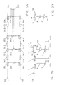
- FIG. 4E describes in detail the circuit of an elementary generator for ordering control of the optical time switches with propagation TSU, such as the circuit 45.f of FIG. 4C.
- the optical input 450 is connected, optionally by means of an optical amplifier 1, to the input of an optical coupler 2 of the one input and two output type.
- the coupler 2 is connected: . by its first output at the first input of an optical switch 3, produced by an optical switch, of a type with two inputs and two electrically controllable outputs, or by an optically controllable optical connection point such as that of FIG. 5B, the control input of which is electrically connected to an access 4534; . and by its second output to an optical delay line 5, the output of which is connected to the optical input of a detector 7.
- the output of the optical switch 3 is optically connected to the optical excitation input 4a of a tunable optical source 4 whose output 4b is optically connected to the output 451 of the elementary generator and the input 4c for controlling tuning is electrically connected to the output of a circuit 6 generating an electrical tuning signal from the optical source 4.
- the circuit 6 is connected by a first control input to the output of a counter 8 and by a second control input to the input 452 of the elementary generator.
- the counter 8 is electrically connected by a first input to the output of the detector 7, moreover connected to an access 4531, by a second input to an access 4532 and by a third input to an access 4533, the said accesses and the access 4534 connected to the control input of the switch 3 forming the multiple access such as 453.f of FIG. 4C connected to the supervisor 49.
- the optical source 4 can be tuned to any frequency Fbj of the fb optical frequencies of the second set Fb of optical frequencies defined during the description of FIG. 1B, fb being at most equal to the maximum number fmax of the technically discriminable optical frequencies in an optical spectrum , for example by the filtering means OF in FIG. 5B.
- FIG. 5A describes an embodiment of an optical time switch with propagation TSU, in which: . 501 and 502 are respectively the input of the switch and the control input of the switch respectively optically connected to one of the outputs of the line explorer LS and to the output of the same rank of the order distributor CD as already described; . 51.1 to 51.k are the k outputs of the switch, each one being optically connected to an input of the optical diffuser OD, which is of a type with (m + (nk)) inputs and s outputs.
- the time switch consists of: - a first optical delay line with multiple taps, formed by the series assembly of k-1 identical optical delay lines 54.1 to 54. (k-1) and k identical optical couplers 53.1 to 53.k, each having an input and a first and a second output and directing on the second output a fraction of the optical energy arriving on the input and on the first output the rest of the optical energy, assembly such as: the input 501 of the switch is optically connected to the input of the coupler 53.1; the first outputs of the couplers 53.1 to 53. (k-1) are each connected to the input of one of the delay lines 54.1 to 54.
- each connection point being optically connected to the second output of the coupler of the same rank of the first multiple tap delay line; its output being connected to the output of the same rank in the group of outputs 51.1 to 51.k; and its control input being connected to the second output of the coupler of the same rank of the second multiple tap delay line.
- FIG. 5B describes an embodiment of a connection point such as 55.1, implemented in the optical time switch with propagation TSU described above, consisting of: - an optical amplifier OA, of the semiconductor type, whose optical input and output are optically connected respectively to the optical input SI and the optical output SO of the connection point; - an optoelectronic detector D whose output is electrically connected to the control input of the optical amplifier OA and the optical input to the optical output of an optical filter OF; - an optical filter OF, tunable to any frequency Fbj of the group Fb of optical frequencies, the optical input of which is connected to the optical control input SC of the connection point.
- a connection point such as 55.1, implemented in the optical time switch with propagation TSU described above, consisting of: - an optical amplifier OA, of the semiconductor type, whose optical input and output are optically connected respectively to the optical input SI and the optical output SO of the connection point; - an optoelectronic detector D whose output is electrically connected to the control input of the optical amplifier
- FIGS. 5C and 5D each describe an embodiment of a time switch TSU having a single output 51.
- the assembly of FIG. 5C implements an optical coupler 58 having k inputs, connected each at the exit of one of the k connection points 55.1 at 55.k and an output connected to output 51 of the TSU switch; and the assembly of FIG. 5D implements k optical couplers 58.1 to 58.k, each having a first, a second inputs and an output.
- Couplers are associated in series by connecting the output of the coupler of rank i to the first input of the coupler of rank i + 1, the first input of the coupler 58.1 not being connected and the output of the coupler 58.k being connected to output 51 of the TSU switch.
- the second input of each coupler is connected to the output of the connection point 55.1 to 55.K of the same rank.
- the optical diffuser OD used in the device SSTSN is of a type having n + m inputs and s exits.
- FIG. 6 schematically represents a communication terminal comprising: a reception circuit 61, of the UR type, connected by its optical input 6100 to an optical fiber 601 for connection to the central SN, supporting the URL link on which are transmitted optically a transmission multiplex CEM configuration and the communication reception multiplex URM ; a transmission circuit 62, of UE type, connected by its optical output 6200 to an optical fiber 602 for connection to the exchange supporting the UEL link on which the spectro-time multiplex communication transmission UEM is transmitted; an optical frequency reference means 63 having an input connected to an output 6104 of the reception circuit 61, a first output connected to an input 6103 of the reception circuit 61 and to an input 6203 of the transmission circuit 62, and a second exit; a control means 64 having an input connected to an output 6105 of the reception circuit 61, a first output connected to an input 6102 of the reception circuit 61 and to an input 6202 of the transmission circuit 62, and a second output; a synchronizable generator of clock signals 65
- Said second outputs of said frequency reference means, control means and synchronizable generator of clock signals are optionally connected respectively to inputs 6103, 6102, 6101 of other reception circuits identical to circuit 61 constituting reception terminals, and / or to other inputs 6203, 6202, 6201 of other transmission circuits identical to the circuit 61 constituting transmission terminals.
- the reception circuit 61 includes: . an optical receiver of configuration 611 tuned to one of the frequencies of the first group of optical frequencies Fa1, receiving said CEM multiplex; . an optical transmission receiver 612, tunable to any of the optical frequencies of the second group of frequencies Fa2, receiving said URM multiplex; . frequency tuning means 613 of the optical transmission receiver 612; . time synchronization means 614 of the received information cells; . a means of processing 615 of the information received.
- the optical configuration receiver 611 is connected by its optical input to the optical input 6100 of the reception circuit, by a first output, delivering an optical frequency reference signal to output 6104 and by a second output delivering the information received from the EMC multiplex at output 6105 of the receiving circuit.
- the optical transmission receiver 612 is connected by an optical input to the optical input 6100 of the reception circuit, by a control input to an output of the frequency tuning means 613, and by an output delivering the information received from the multiplex.
- URM to an input of the time synchronization means 614.
- the time synchronization means 614 is connected by an output to an input of the operating means 615.
- the frequency tuning means 613, time synchronization 614 and operating 615 are each connected by a control input to the input 6102 of the reception circuit 61, the time synchronization 614 and operating 615 means being also each connected by a synchronization input to the input 6101 of the reception circuit and the frequency tuning means 613 being itself connected by a frequency reference input to the input 6103 of the reception circuit.
- the transmission circuit 62 comprises: . a transmission optical transmitter 621, tunable to any of the optical frequencies of the second group of frequencies Fa2; . frequency tuning means 622 of the optical transmission transmitter; . time synchronization means 624 of the information cells to be transmitted; . a source means 625 of the information cells to be transmitted, . a time framing means 623.
- the optical transmission transmitter 621 is connected by an optical output to the optical output 6200 of the transmission circuit, by a control input to an output of the frequency tuning means 622, and by a signal input to an output of the time synchronization means 624 transmitting the information cells to be transmitted optically in the UEM multiplex.
- the time synchronization means 624 is connected by an input to an output of the source means 625 and by a synchronization input to a first output of the time alignment means 623, a second output of which is connected to a synchronization input of the tuning means frequency 622.
- the frequency tuning means 622, time framing 623 and source 625 are each connected by a control input to the input 6202 of the transmission circuit 62, the framing means time 623 and source 625 also being each connected by a synchronization input to the input 6201 of the transmission circuit and the frequency tuning means 622 being itself connected by a frequency reference input to the input 6203 of the circuit resignation.
- the communication system of the invention is configured as follows: .
- the CPU management means (Fig. 1) is connected to the SSTSN device by a single link of each of the CEL, SEL, CRL, SRL types, each carrying a CEM or SEM or CRM or SRM multiplex;
- the terminals connected to the central SN are communication terminals, each comprising: .. a transmission circuit UE transmitting on its transmission link UEL a spectro-time transmission multiplex transmission UEM by means of a tunable transmission optical transmitter; ..
- reception circuit UR receiving by the reception link URL the configuration multiplex CEM and a reception multiplex URM, the reception circuit UR having an optical configuration receiver and an optical transmission receiver; .. and various other functional means including optical frequency tuning means of said optical transmitters and receivers, a synchronizable generator of clock signals, a time synchronization means and a time framing means of the transmission circuit, a synchronization means time of the reception circuit, and a control means supervising the various other functional means.
- each channel has a duration T, .
- the frame gathers c channels, .
- the period of the frame is equal to cT, .
- the first channel of each frame carries an identification code for the start of the frame, as is known in time techniques, .
- the other channels are undifferentiated, they are used by CPU to transmit the configuration messages to the terminals; - the CRM, SEM, SRM, UEM and URM multiplexes are organized into a series of undifferentiated time channels of duration T; the undifferentiated time channels convey the information to be transmitted in the form of optical samples of duration T having temporally three parts of which only the second part carries the transmitted information, the first and third parts constituting switching windows avoiding having to frame perfectly the samples to be switched in the local time system of the switching device SSTSN; - the information to be transmitted, when it is digital, is formatted in cells which are each conveyed by an optical sample; - the optical samples are encoded on transmission at an optical frequency characteristic of their destination, with the exception of the samples of broadcast multiplexes, such as the CEM multiplex, which are all optically encoded at a frequency characteristic of the configuration function; - the SSTSN spectro-temporal switching device: .
- the CEM multiplex is broadcast on each reception link and received by the optical receiver for configuring the reception circuits CR, SR, UR, and the CRM, SRM or URM multiplexes sent on the CRL or SRL or URL links are respectively received optically by the optical receiver for transmitting the reception circuits CR or SR or UR.
- the optical transmitter of the transmission circuit CE the optical receiver for configuring the reception circuits CR, SR and UR are tuned to the optical frequency Fa1.1 and all the filters WF are adjusted to be transparent at this optical frequency; - the optical receiver for transmitting the CR and SR reception circuits, and the WF filters connected to the CRL and SRL links are tuned to the frequencies Fa2.1 and Fa2.2 respectively.
- the clock signal generators of the terminals synchronize with the central office synchronization signal generator CKU; . the terminals have a frequency reference allowing the operation of the optical frequency tuning means of their optical transmission transmitters and receivers; the terminals can then be initialized by the control means CPU of the connection center.
- the generator synchronization signals CKU permanently transmits on the link H2 a clock signal of period T, delimiting the time channels, and a clock signal of period cT, delimiting the frames, which signals are used by the control means CPU to temporally format the multiplex EMC.
- the CEM multiplex is emitted by the optical transmitter of the transmission circuit CE at the optical frequency Fa1.1 on the CEL link and broadcast by the optical diffuser OD of the space-time spectro switching device SSTSN, the filters WF being transparent to the frequency Fa1.1, on all the reception links, in particular the URL links, connected to the SSTSN device.
- the configuration receiver of each reception circuit permanently receives the CEM multiplex.
- the start of frame identification code routed by the first channel of the CEM multiplex, is used by clock signal generators of the terminals to synchronize with the pilot clock of the synchronization generator CKU of the central SN according to known methods in time systems.
- Each local clock signal generator transmits, among other things, to the means for synchronizing the transmission and reception circuits of the terminal a channel synchronization signal.
- the optical frequency Fa1.1 of the CEM multiplex is used by the frequency tuning means of the terminals as a reference frequency for tuning the optical transmitters and optical receivers for transmission of the transmission and reception circuits on the frequencies of group Fa2 of the frequencies optical.
- the CPU control means When the system is put into service and each time a terminal is put into service, an initialization procedure for each terminal to be put into service is launched by the control means CPU.
- the CPU control means : . assigns a frequency Fa2.i to the reception circuit UR of the terminal to be initialized; . positions, in SSTSN and via the filter configuration circuit FCC, the filter WF connected to the link URL of the terminal to be initialized on said frequency Fa2.i; . transmits to the initialization terminal, by the CEM multiplex, an initialization message containing: .. the identity of the terminal, .. a code designating the initialization function, .. the references Fa2.1 and Fa2.2 of the optical frequencies carrying the CRM and SRM multiplexes, .. the reference of the optical frequency Fa2.i temporarily assigned to the UR receiving circuit of the terminal.
- the control means of the terminal on initialization grants the optical receiver for transmission of the reception circuit to the optical frequency Fa2.i and proceeds to the adjustment of the time framing means of the synchronization circuit of the circuit d 'program.
- the time alignment means phase the channel clock received from the local clock signal generators so that the time channels of the UEM multiplex, temporally positioned by the phase shift channel clock, appear at the input of the switching device SSTSN of the central office in phase with the channel clock of said SSTSN device, the temporal alignment of the channels however not having to be perfect due to the temporal organization of the optical samples as indicated previously.
- the phase shift of the channels at the input of SSTSN is at least equal to the sum of the propagation times of the optical samples of the CEM multiplex on the URL link and of the UEM multiplex on the UEL link.
- the procedure for adjusting the framing means implements the following sequence of operations: . recording a phase shift value in the time-setting means of the synchronization circuit of the transmission circuit; . transmission of a framing code in the form of an optical sample encoded by the optical transmitter at the optical frequency Fa2.i, in a channel of the multiplex UEM synchronized with the phase-shifted clock originating from the framing means; . switching of the sample by the SSTSN device, and transmission in the first time-accessible channel of the URM multiplex of frequency Fa2.i; . reception of the code switched by the reception circuit of the terminal, and control of the code received.
- This sequence is repeated by increasing with each new sequence the registered value of the phase shift, until the code received, degraded by the switching as long as the phase of the sample is bad at the input of the switching device SSTSN, be correct.
- the value of the phase shift which enabled the first correct transmission is recorded by the control means of the terminal and the procedure is continued by increasing the value of the phase shift until an incorrect transmission is obtained.
- This new phase shift value is recorded and the time alignment means is then adjusted by the terminal control means to the average value of the two recorded phase shift values. The terminal is therefore operational.
- the terminal sends a message via its UEM multiplex signaling that the framing has been carried out, carried by optical samples encoded at the frequency Fa2.1 designated as that of the CRM multiplex, which samples are, after switching in SSTSN transmitted on the CRM multiplex and received by the CPU control means.
- the CPU On receipt of the "framing performed" code, the CPU sends a control message to the terminal, encoded at the frequency Fa2.i, transmitted in the SEM multiplex on the SEL link and then routed by SSTSN in the URM multiplex of the terminal.
- the terminal responds to CPU by sending in its UEM multiplex a message, containing the control code received, optically encoded at the frequency Fa2.2, designated as that of the SRM multiplex, which message, switched by SSTSN in the SRM multiplex on the SRL link, is received by CPU.
- the CPU control means On receipt of this last message, and after checking the code received in return, the CPU control means: . sets at rest, via the FCC circuit for configuring the filters, the WF filter connected to the URL link serving the terminal, previously tuned to the frequency Fa2.i; . command, by a message encoded at the frequency Fa1.1 and transmitted in the CEM multiplex, putting the terminal on standby which, upon reception, positions the optical transmission receiver of its reception circuit at rest, acknowledges reception to the CPU by a message transmitted in the UEM multiplex at the frequency Fa2.1 designated by the CRM multiplex and goes into standby position, which consists of permanent listening to the CEM multiplex by means of the optical receiver for configuring its reception circuit, tuned to the frequency Fa1.1; . and, upon receipt of the message from the terminal, releases the optical frequency Fa2.i.
- a terminal in the standby state having to establish a communication with another terminal, transmits on its UEM multiplex, at the frequency Fa2.1 designated as the access frequency of the CRM multiplex, a message to the CPU, containing its identity and a request for allocation of reception frequency.
- the CPU assigns a frequency Fa2.j to the terminal, grants the WF filter giving access to the reception link URL of the terminal on the said allocated frequency and transmits to the terminal by message sent by the CEM multiplex the reference of the frequency Fa2.j allocated.
- This frequency Fa2.j is kept by the terminal throughout its period of activity.
- the terminal transmits on its UEM multiplex at the frequency Fa2.1 designated as the access frequency of the CRM multiplex, an end of activity message to the CPU, containing its designation and the reference Fa2 .j of the frequency to be released, and goes to standby.
- the CPU positions the WF filter connected to the terminal's URL link at rest and releases the frequency Fa2.j.
- Any terminal positioned in activity having to establish a communication transmits to CPU, by the multiplex SRM, a call message containing its identity and that of the requested terminal. If the requested terminal is not active, the CPU assigns this terminal a free receiving frequency Fa2.k, grants the WF filter connected to the URL link of this terminal on the frequency Fa2.k, and transmits to the terminal requested by the CEM multiplex a message from activation, containing the identity of the terminal requested, the order of activation and the reference of the frequency Fa2.k allocated.
- the requested terminal having detected the message and having positioned itself, acknowledges receipt to the CPU by an optically encoded message at the frequency Fa2.1 which is routed by SSTSN in the CRM multiplex on the CRL link from which it is received by the CPU.
- the control means CPU then transmits to the requesting terminal the reference of the frequency Fa2.k allocated to the called party, by a message encoded at the frequency Fa2.j of the requester, transmitted in the multiplex SEM on the link SEL and routed by SSTSN in the URM multiplex on the requester's URL link accessible by the frequency Fa2.j.
- the CPU transmits, as soon as received the request, by the SEM multiplex the reference of the frequency Fa2.k already allocated to the requested terminal.
- the requesting terminal can send to it a call message encoded at the frequency Fa2.k containing the designation of its own reception frequency Fa2.j. If the requested terminal does not respond, the requesting terminal renews the procedure.
- the same terminal can, at a given time, be in communication with a multiplicity of different terminals.
- a terminal j to which the access frequency Fa2.j has been allocated, in communication with a terminal v, whose access frequency is Fa2.v, and another terminal w, whose access frequency is Fa2.w.
- the information cells, relating to communications (j / v) and (j / w), are statistically multiplexed at the input of the transmission circuit of terminal j and transmitted in the multiplex UEM.j on the link UEL.j by the optical transmitter of the transmission circuit in the form of optical samples respectively encoded at the frequency Fa2.v or Fa2.w, characteristic of their destination.
- the optical samples encoded at the frequency Fa2.v and the optical samples encoded at the frequency Fa2.w, coming from the multiplex UEM.j, are first shifted in time by the same switch TSU.j to be placed each in the first free channel of their destination multiplex, the multiplex URM.v for the first and the multiplex URM.w for the second; the shifting of the first is carried out under the control of the elementary command order generator 45.v, the shifting of the second under the control of the elementary command order generator 45.w from the group of elementary command generators 45.1 to 45. f of Figure 4C.
- these samples are spectrally selected by the filters WF.v and WF.w and transmitted, the first in the URM.v multiplex on the link URL.v which transmits them to the terminal v, the second in the URM.w multiplex on the link URL.w which transmits them to terminal w.
- the samples are received by the optical transmission receiver of the terminal reception circuit tuned to their optical carrier frequency.
- the information cells relating to the communication (v / d), statistically multiplexed with other different destination cells, are transmitted by the transmission circuit of the terminal v in its multiplex UEM.v on its link UEL.v under the form of optical samples, encoded at the frequency Fa2.j of access to the terminal j.
- the information cells relating to the communication (w / d), statistically multiplexed with other cells of different destination, are transmitted by the transmission circuit of the terminal w in its multiplex UEM. w on its UEL.w link in the form of optical samples, encoded at the frequency Fa2.j of access to the terminal j.
- the optical samples encoded at the frequency Fa2.j, coming from the multiplexes UEM.v and UEM.w, are successively shifted in time by the switches TSU.v and TSU.w, under the control of the same elementary command order generator 45.j from the group of elementary command generators 45.1 to 45.f of FIG. 4C, to be placed each, in the destination multiplex URM.j, in the first channel deemed free at the time of the command to control their time switching.
- the switches TSU after broadcasting by the broadcaster OD, they are spectrally selected by the filter WF.j and transmitted in the multiplex URM.j on the link URL.j which transmits them to the terminal j. In this terminal, they are successively received by the optical transmission receiver of the reception circuit tuned to the frequency Fa2.j.
- the cells transmitted by the various terminals each include a code identifying the communication concerned to allow their exploitation at the output of the reception circuit, which is well known in the technique of asynchronous transfer.
- the charging of communications is carried out by the central control means CPU.
- the CPU has the references of the communicating terminals, obtained during the establishment of the communications, and the data of a measurement of the flow of optical samples carried out by the circuit 49 of FIG. 4C, by means of counters of flow activated by a counting signal defined in the description below of the detailed operation of the switching device SSTSN, which data include: . the reference of the source and the reference of the destination, which are respectively deduced by the circuit 49 from the time reference of the counting signal coming from the OLM multiplex, and from the reference of the generator 45.i having delivered the counting signal; . the output status of a flow meter assigned to monitoring communication defined by the two previous references.
- the contemporary channels of the various spectro-time transmission multiplexes are present on the inputs I1 to In of SSTSN temporally in phase, between them and with respect to a local clock of the synchronization signal generator CKU of the central SN (fig. 1A).
- Ti and T are respectively the time reference and the duration of a channel of the transmission multiplexes, n is the number of inputs of the line explorer.
- This exploration pulse received on the input 201 of the circuit of FIG.
- 3B propagates in said third control device, time shifted by a duration t by each of the delay lines 231.1 to 231.n, by successively controlling the optical switches 224.1 to 224.n of said optical selector. These switches each successively transmit on output 203, by formatting it at time t, an optical signal called "address signal".
- This address signal is split by each switch such as 224.1 in the signal present on its input, which present signal consists of the part of energy taken by the associated coupler, such 226.1, from the optical sample of the transmit multiplex present on the input of the optical selector, such as 210.1, during the instant Ti, part of energy which is possibly amplified and calibrated in level by the amplifier such as 225.1.
- n successive address signals transmitted on the output 203 during the instant Ti constitute the useful part of a frame of the multiplex OLM described in the description of FIG. 1B, which frame comprises n + 2 channels of which the first and last are used for time frame of the multiplex.
- the rank r of an address signal in the n address signals of the same frame is characteristic of the source of the optical sample of the transmission multiplex from which the address signal is derived.
- the optical carrier frequency Fa2i of each of these n address signals is characteristic of the destination of the optical sample of the transmission multiplex from which the address signal is derived.
- the optical address signal coming from the spectral demultiplexer is: . applied to entry 450, . amplified by optical amplifier 1, . temporally calibrated by the optical switch 3 excited by a clock signal of period t, delivered by the supervisor 49 of FIG. 4C on the link 4534, clock signal whose form factor is such that it allows inhibit the transient states between the successive optical address signals, and, part of its energy having been taken up by the coupler 2 and emitted in the delay line 5, is present on the input 4a of the optical source 4.
- the optical source 4 tunable to any frequency of the fb optical frequencies of the second set Fb of optical frequencies, is positioned by means of the tuner signal generator 6 to transmit on the frequency Fbj designated by the information present at the output of the counter 8.
- the designated frequency Fbj is characteristic on the one hand of the real time delay to be introduced into the propagation of the optical sample to be switched, from which the optical address signal coming from the input 4a is derived, to allow its insertion in the first channel free from the destination receiving multiplex, and on the other hand from the connection point to be excited in the TSU switch (Fig. 5A, 5B or 5C) processing the optical sample.
- the optical source 4 of FIG. 4E transmits on its output 4b, for the whole duration of this address signal, that is to say for a duration at most equal to t, an optical signal for controlling the switch.
- the output pulse of the detector 7 is moreover emitted by the link 4531 to the circuit 49 of FIG. 4C which exploits it on the one hand as part of a process of permanent monitoring of the bit rates of the different terminals, known as the procedure "sentinel"; and on the other hand as a counting signal for the incrementation of debit counters whose states are periodically transmitted to the CPU control means which uses them for the charging of communications.
- a counter 8 displays a value Fbj + 1 different from the minimum value FbO, at the start of the instant Ti + 1, the counter is positioned at the value Fbj; and if it displays the minimum value FbO, it remains positioned on this value FbO.
- the circuit 49 positions the counters 8 in the initial state (such as FbO), by the link 4533 whose other functions have been described above.
- the successive control orders issued by the various elementary generators such as 45.f in FIG. 4C are routed by the coupler 46 and the adjustable delay line 42, on the output 411 where they follow one another and constitute the part active of a frame of the CLM control order multiplex, which includes, like that of the OLM multiplex from which it comes n + 2 channels, the first and last of which are used for time framing of the multiplex, and the n others carry any control commands.
- d is the duration of the operations described above for developing a control order, measured between the appearance of the exploration pulse on the second output of the coupler 221.1 of said "third control device" in FIG. 3B and the appearance at the input of the delay line 42 of the control order, coming from the address signal created by the switch 224.1 controlled by the output of this coupler 221.1, the delay line will be adjusted to the delay value td.
- the delay line 42 is adjusted to the delay value 0, the delay lines such as 231.1 and 331.1 of FIG. 3A respectively value delay d and td.
- the arrangement described in FIGS. 3A or 3B is not implemented. It is replaced by an assembly associating the circuits described in FIGS. 2A and 2B, which are controlled by the control circuit described in FIG. 4A, in place of the circuit 4B mentioned above.
- the delay line 424 of Figure 4A has a delay value equal to d and the delay line 42 of Figure 4C has a zero delay value.
- the CLM multiplex is sent from the output 411 of the generator of the control orders of FIG. 4C on the input 303 of the distribution line of FIG. 3B in which it propagates.
- the switches 324.1 to 324.n switch to the hysteresis amplifier, such as 325.1, connected to their second output, the control order carried by the channel CLM multiplex contemporary with their control impulse.
- the hysteresis amplifier such as 325.1, receiving a control order of duration close to t and carried by the optical frequency Fbj, displays on its output an optical signal of the same frequency Fbj and of duration equal to T, which signal is then delayed by the delay line such as 326.1 by a duration equal to (n + 1-r) t, r being the rank of the delay line concerned in the group of n delay lines 326.1 to 326.n.
- control orders carried out during the channel instant Ti of the transmission multiplexes exit in phase at Ti + 1, each on one of the outputs 311.1 to 311.n of the distribution line.
- UDM spectro-temporal emission multiplexes
- Each optical sample and the associated control order are therefore in phase, respectively on the input 501 and the control input 502 of the time switch TSUr connected to the outputs 211.r of the circuit LS and 311.r of the circuit CD.
- this switch TSUr like the switch TSU represented in FIG. 5, they propagate in phase, respectively in the first and second multiple-tap delay lines of the time switch TSU, delayed by a time T by each of the elementary delay lines crossings, such as 54.1 and 57.1.
- each coupler such as 53.1 takes a share of the energy of the optical sample which passes through it and therefore presents a similar signal at the level of the connection point such as 55.1 which is connected to it. energy close to the incident optical sample and in particular of the same optical frequency Fa2i.
- each coupler such 56.1 takes a part of the energy of the control order which passes through it and therefore presents on the control input of the connection point such 55.1 which is connected to it a signal which has the same optical frequency Fbj and the same duration as the incident command order.
- the control signal passes through the coupler 56.j, the signal picked up causes the connection point 55.j to operate on the control frequency Fbj according to the mechanism already described above (fig. 5A).
- the signal from the optical sample present at this time at the input of the connection point is therefore amplified and transferred to the output of the connection point where it reproduces the incident optical sample and constitutes the switched optical sample.
- the switched optical sample is presented by output 51.j (fig.5A) or output 51, via coupler 58 (fig.5C) or from the series of couplers 58.j to 58.k (fig .5D), at the entrance to the OD optical diffuser (fig. 1B).
- a multiplicity of samples, carried by different optical frequencies, propagating in the same switch TSU, can be switched simultaneously and can therefore occur simultaneously on or at the output of the switch.
- the optical diffuser OD spectrally multiplexes all the switched optical samples coming from the outputs of the switches TSU, each carried by a frequency optical different from the group Fa2 of the optical frequencies, and the optical signals coming from the accesses Ic and Ib, respectively carried by one of the optical frequencies either of the group Fa1 of the optical frequencies or of the group Fa3 according to the type of access, and diffuses on each of its outputs a spectral multiplex formed of all the samples and optical signals presented on its inputs, the energy of each signal or incident sample being equally distributed between all the outputs.
- the optical amplifier filters WF such as WF1, each connected to an output of the diffuser, transparent for the optical frequencies of the groups Fa1, possibly tuned to one or more of the frequencies Fa3, and each tuned to a particular frequency of the group of the frequencies Fa2, or a frequency band of the frequency group Fa2 as already explained in the description of FIG.
- a first embodiment of the SSTSN spectro-time switching device comprising n optical time switches with controlled propagation TSU, each associated with an input line, each consisting of: a first and a second multiple tap delay lines in which the samples to be switched and the switching orders are propagated in synchronism, and of a multiplicity of optically controlled connection points, each connected by an input to an output of said first delay line, and by a control input to an output of said second delay line, the outputs of the connection points being connected to the outputs of the switch.
- TSU time switches are of the output control type.
- FIG. 7 schematically represents a second embodiment of the spectro-temporal switching device SSTSN of FIG. 1A.
- optical time switches with controlled propagation, TSU1 to TSUn, of the first embodiment are replaced by optical time switching means, MTSU; the other means used are the same as the various other means of said first embodiment, namely: . I1 to In, Ib and Ic are optical inputs. . O1 to Oq, On and Oc are optical outputs. . H1 and CB are a synchronization link and a control link of the spectro-space-time switching device SSTSN. . LS is an optical circuit exploring input lines. .
- CC is a control circuit for the spectro-space-time switching device.
- CD is an optical circuit for distributing control orders.
- OD is an optical diffuser.
- WF1 to WFs are optical filters.
- FCC is a configuration circuit for filters WF1 to WFs.
- the optical propagation time switching means MTSU of this device SSTSN have: . n inputs 501.1 to 501.n each optically connected to one output 211.1 to 211.n of the optical circuit exploring the LS input lines; . n control inputs 502.1 to 502.n each optically connected to an output 311.1 to 311.n of the optical circuit distributing the CD control orders; . and optical outputs L51 each optically connected to an input of the optical diffuser OD.
- Said optical means of time switching with propagation MTSU consist of: . n input circuits DUIC.1 to DUIC.n, each having an optical input optically connected by one of the inputs 501.1 to 501.n to an output of the optical scanning circuit LS, an optical control input optically connected by one of the control inputs 502.1 to 502.n at an output of the optical distributor of the CD control orders; . and an output device DUOC optically connected at the input to the input circuits DUIC.1 to DUIC.n, and by each of its outputs to the optical diffuser OD.
- FIG. 8A schematically represents an embodiment of a DUIC input circuit, in which: . 70.1 and 70.2 are respectively an optical input and control input optically connected to the outputs of the line explorer LS and of the CD command distributor as already described. . 71.1 to 71.k are k optical outputs, optically connected to inputs of the DUOC output device according to the various arrangements described below by FIGS. 4A to 5B.
- the DUIC input circuit consists of: . of an optical diffusion optical device produced by the serial assembly of k optical couplers 73.1 to 73.k each having an input, a first and a second output, the couplers being placed in series by connecting the input of the one at the first output of the next except for a last coupler 73.k whose input is connected to input 70.1 of the input circuit; . k optically controlled optical connection points 74.1 to 74.k, each connection point 74.i having an input connected to the second output of the same rank optical coupler 73.i and an output connected to the same rank output 71.i of the input circuit and an optical control input; . and a spectral demultiplexer 72 having an optical input connected to the control input 70.2 of the input circuit and k outputs 721.1 to 721.k each connected to the optical control input of the connection point 74.i likewise rank.
- FIG. 8B schematically represents an alternative embodiment of a DUIC input circuit, having an optical optical diffusion device, k optical connection points optically controlled 74.1 to 74.k and a spectral demultiplexer 72, in which the optical device of optical diffusion consists of an optical coupler 75 having an input 750 connected to the input 70.1 of the input circuit and k outputs 751.1 to 751.k each connected to the input of the connection point 74.i of the same rank , all the other provisions being identical to the similar provisions already described in FIG. 8A.
- FIG. 9A schematically represents the production of an optical delay line with multiple inputs OMIDL, used in the output device DUOC.
- This multiple input optical delay line has k optical inputs 80.1 to 80.k and an optical output 81 optically connected to an input of the optical diffuser OD; and consists of the serial assembly of k-1 identical elementary optical delay lines 83.1 to 83. (k-1), k-1 optical couplers 82.1 to 82. (k-1) and an optical amplifier 84 with large spectral band having an input and an output.
- Each optical coupler 82. has a first input connected by a delay line 83.i to an output of the following optical coupler, with the exception of a last coupler 82.
- FIG. 9B schematically represents the production of a OMIDC multiple input delay optical circuit used in the DUOC output device.
- This multiple-input optical delay circuit has k optical outputs 81.1 to 81.k each optically connected to an input of the diffuser OD, and k optical inputs 86.1 to 86.k; and consists of k different optical delay lines 85.1 to 85.k and k broadband optical amplifiers 84.1 to 84.k. Each amplifier has an input and an output.
- Each optical delay line 85. has an input connected to the input of the same rank 86.i of the OMIDC circuit. and an output connected to the input of the same rank optical amplifier 84.i whose output is connected to the same rank output 81.i of the OMIDC circuit.
- Each delay line 85.i achieves a delay whose value is a function of its rank.
- FIGS. 10A and 10B each represent a variant of a first mode of organization of the optical time switching means with propagation MTSU consisting of n input circuits DUIC.1 to DUIC.n, and of an output device DUOC.
- the DUOC output device consists of n temporal rearrangement means each associated with a DUIC.i input circuit, which are: . in the assembly of FIG. 10A: n optical delay lines with multiple inputs OMIDL.1 to OMIDL.n of the type described by FIG. 9A; . and in the assembly of FIG. 10B: n multiple input optical delay circuits OMIDC.1 to OMIDC.n of the type described in FIG. 9B.
- each OMIDL.i multiple input optical delay line or each OMIDC.i multiple input optical delay circuit is associated with a DUIC.i input circuit, the outputs 71.1 to 71.k of said circuit input being optically connected to the same rank input 80.1 to 80.k of the associated OMIDL.i delay line (Fig.10A) or to the same rank input 86.1 to 86.k of the OMIDC.i delay circuit associated (Fig. 10B).
- FIGS. 11A and 11B each represent a variant of a second mode of organization of the optical switching means temporal propagation MTSU. They consist of n DUIC.1 to DUIC.n input circuits and a DUOC output device.
- the DUOC output device consists of: . k optical combiners 9.1 to 9.k each having n optical inputs 90.1 to 90.n and an output 91, each combiner being connected optically as an input to each of the input circuits DUIC.1 to DUIC.n, the input 90 .j of a combiner 9.i being connected to output 71.i of an input circuit DUIC.j; . and a unique means of temporal rearrangement, which is: .. in the assembly of FIG.
- Each transmission link UEL and SEL routes in channels of duration T an optical sample constituting a transmitted message, whose optical frequency Fa2.i is characteristic of a destination link.
- the exploration circuit LS performs a destination multiplex OLM by sampling the channels presented on its inputs I1 to In by the transmission links UEL and SEL.
- the frame of the OLM multiplex has the same duration T as the input channels and a number of useful channels at least equal to the number of transmission links.
- the control circuit CC From the signals of the OLM multiplex and as a function of the load of the destination links, the control circuit CC develops control commands for switching the optical samples.
- - Said control orders each consist of an optical signal at an optical frequency Fbi, of a second set of optical frequencies Fb, each optical frequency of which is characteristic of a propagation delay in real time which must undergo, in the optical means time switching, the sample to be switched, and is also characteristic of the address of an optically controlled connection point in the switching means.
- - Said control orders are multiplexed into a multiplex of CLM control orders, the frame of which is identical to the frame of the OLM multiplex and each channel of which is associated with a transmission link and sends to Ti a switching order relating to the sample transmitted in the channel of the transmission link during the time Ti.
- the exploration circuit LS transmits on its outputs 211.1 to 211.n the samples presented to Ti on its inputs by the transmission links, and the optical distributor CD transmits on each of its outputs 311.1 to 311.n the switching control orders for these samples, the said samples and control orders having the same duration T.
- An input circuit DUIC.i receives on its input 501.i a sample to be switched and on its input 502.i the command to switch said sample; below, the sample to be switched and the control order are assumed to be carried respectively by the optical frequency Fa2.i and by the optical frequency Fbj. .
- the sample is presented (Fig.8A) at input 70.1 of the optical diffusion device which distributes a representative signal at the input of each of the optically controlled connection points 74.1 to 74.k. .
- the control order is presented at input 70.2 of the spectral demultiplexer which switches it as a function of its optical frequency Fbj on output 721.j which transmits it to the control input of the point connection 74.j, for the duration T of the order.
- the connection point 74.j is active so that the sample signal present on its input propagates from its input to the output 71.j. . From this output, by the combiner 9.j (Fig.11A), the sample arrives at input 80.j of the optical delay line with multiple inputs OMIDL, into which (Fig.9) it is transferred by the 82.j coupler in the optical delay line. It propagates, delayed by a duration T by each elementary optical delay line crossed. .
- the sample amplified by the optical amplifier 84 appears on the output 81 then propagates in the diffuser OD which diffuses it on all its outputs where it is selected and amplified by the WFi filter tuned on its carrier optical frequency Fa2.i, then transmitted on the destination link.
- the communication system according to the invention by virtue of the fact that it transmits and switches the communication signals only by optical means, avoids the use of electro-optical and opto-electric conversion devices between the means of optical transmission and the switching means existing in currently known asynchronous time systems. It thus allows an economy of means, a simplification of the structure of the communication networks and consequently a simplification of the operation and an improvement of the overall reliability.
- the entire switching device Because it uses only optical technology for the production of the switching means, and because of the simplicity of the means and mechanisms used, the entire switching device, including its control operating under the sole control of a clock signal and optical signals directly from the samples to be switched, it offers original and economical solution to complex ATM switching problems.
- the system according to the invention thus marks real progress with respect to the prior art for equipping broadband multiservice communication networks, by the facilities it offers for the organization of said networks, by the economy means it allows, and the security it provides in the transmission of information signals.
Landscapes
- Engineering & Computer Science (AREA)
- Computer Networks & Wireless Communication (AREA)
- Signal Processing (AREA)
- Optical Communication System (AREA)
- Use Of Switch Circuits For Exchanges And Methods Of Control Of Multiplex Exchanges (AREA)
- Data Exchanges In Wide-Area Networks (AREA)
- Time-Division Multiplex Systems (AREA)
Applications Claiming Priority (4)
| Application Number | Priority Date | Filing Date | Title |
|---|---|---|---|
| FR8912842 | 1989-10-02 | ||
| FR8912842A FR2652691B1 (fr) | 1989-10-02 | 1989-10-02 | Systeme de communication optique temporel asynchrone. |
| FR9004034A FR2660500B2 (fr) | 1990-03-29 | 1990-03-29 | Systeme de communication optique temporel asynchrone. |
| FR9004034 | 1990-03-29 |
Publications (2)
| Publication Number | Publication Date |
|---|---|
| EP0421325A1 true EP0421325A1 (de) | 1991-04-10 |
| EP0421325B1 EP0421325B1 (de) | 1995-08-16 |
Family
ID=26227579
Family Applications (1)
| Application Number | Title | Priority Date | Filing Date |
|---|---|---|---|
| EP90118812A Expired - Lifetime EP0421325B1 (de) | 1989-10-02 | 1990-10-01 | Asynchrones optisches Zeitmultiplex-Kommunikationssystem |
Country Status (13)
| Country | Link |
|---|---|
| US (1) | US5105292A (de) |
| EP (1) | EP0421325B1 (de) |
| JP (1) | JP2818481B2 (de) |
| KR (1) | KR0168417B1 (de) |
| CN (1) | CN1018882B (de) |
| AT (1) | ATE126636T1 (de) |
| AU (1) | AU633147B2 (de) |
| CA (1) | CA2026658C (de) |
| DE (1) | DE69021678T2 (de) |
| DK (1) | DK0421325T3 (de) |
| ES (1) | ES2076272T3 (de) |
| MX (1) | MX172650B (de) |
| RU (1) | RU2101867C1 (de) |
Cited By (1)
| Publication number | Priority date | Publication date | Assignee | Title |
|---|---|---|---|---|
| EP2538341A1 (de) * | 2011-06-23 | 2012-12-26 | ONERA (Office National d'Etudes et de Recherches Aérospatiales) | Verfahren zur Berechnung der Wahrscheinlichkeitsverteilung der Übertragungsdauer eines Multiplex-Kommunikationsumschalters |
Families Citing this family (36)
| Publication number | Priority date | Publication date | Assignee | Title |
|---|---|---|---|---|
| US5477364A (en) * | 1989-07-21 | 1995-12-19 | British Telecommunications Public Limited Company | Data transmission on optical networks |
| US5303078A (en) * | 1990-12-18 | 1994-04-12 | Bell Communications Research, Inc. | Apparatus and method for large scale ATM switching |
| FR2672178B1 (fr) * | 1991-01-29 | 1994-03-18 | Alcatel Cit | Concentrateur photonique. |
| US5361255A (en) * | 1991-04-29 | 1994-11-01 | Dsc Communications Corporation | Method and apparatus for a high speed asynchronous transfer mode switch |
| US5528406A (en) * | 1991-08-02 | 1996-06-18 | Gpt Limited | Telecommunications switching device |
| FR2683962B1 (fr) * | 1991-11-19 | 1994-03-25 | Lecoquil Emile | Repartiteur optique. |
| FR2690801B1 (fr) * | 1992-04-29 | 1994-10-28 | France Telecom | Multiplexeur à insertion et extraction. |
| US5418785A (en) * | 1992-06-04 | 1995-05-23 | Gte Laboratories Incorporated | Multiple-channel token ring network with single optical fiber utilizing subcarrier multiplexing with a dedicated control channel |
| IT1257546B (it) * | 1992-06-15 | 1996-01-30 | Cselt Centro Studi Lab Telecom | Commutatore ottico per reti a commutazione veloce di cella. |
| DE4221188C2 (de) * | 1992-06-27 | 1997-09-11 | Sel Alcatel Ag | Vermittlungsstelle |
| US5291324A (en) * | 1992-11-24 | 1994-03-01 | At&T Bell Laboratories | Comparison apparatus with freespace optical interconnections between optoelectronic integrated circuits |
| US5402256A (en) * | 1994-03-31 | 1995-03-28 | At&T Corp. | Optical time slot interchanger apparatus and method of operation |
| IT1273098B (it) * | 1994-03-31 | 1997-07-04 | Cselt Centro Studi Lab Telecom | Dispositivo per il riallineamento di fase di celle atm in nodi atm ottici |
| JP3516490B2 (ja) * | 1994-10-04 | 2004-04-05 | 富士通株式会社 | 回線インタフェース装置 |
| JPH09181774A (ja) * | 1995-12-23 | 1997-07-11 | Nec Corp | 光スイッチ装置及び光スイッチ制御方式 |
| US5729548A (en) * | 1995-12-29 | 1998-03-17 | Telefonaktiebolaget Lm Ericsson (Publ.) | High-speed optical data switching system |
| KR100418251B1 (ko) * | 1996-08-12 | 2004-03-30 | 삼성탈레스 주식회사 | 전파탐지장치(beacon) |
| US6151336A (en) * | 1998-02-11 | 2000-11-21 | Sorrento Networks, Inc. | Time division multiplexing expansion subsystem |
| US6400478B1 (en) | 1998-04-02 | 2002-06-04 | Sorrento Networks, Inc. | Wavelength-division-multiplexed optical transmission system with expanded bidirectional transmission capacity over a single fiber |
| US6298103B1 (en) | 1998-06-16 | 2001-10-02 | Sorrento Networks Corporation | Flexible clock and data recovery module for a DWDM optical communication system with multiple clock rates |
| AU2001238036A1 (en) * | 2000-02-16 | 2001-08-27 | Cymer, Inc. | Process monitoring system for lithography lasers |
| US6904784B2 (en) * | 2001-02-27 | 2005-06-14 | Teledyne Isco, Inc. | Liquid chromatographic method and system |
| CN1161901C (zh) * | 2001-05-14 | 2004-08-11 | 华为技术有限公司 | 光通信系统中上行高速数据的同步接收方法与电路 |
| EP1271825A1 (de) * | 2001-06-25 | 2003-01-02 | Lucent Technologies Inc. | Verfahren und System zur Übertragung von multiplexierten optischen Nachrichten |
| CN1222821C (zh) * | 2002-07-01 | 2005-10-12 | 华为技术有限公司 | 基于波分复用层的光通道保护装置及方法 |
| CN1277375C (zh) * | 2003-07-31 | 2006-09-27 | 华为技术有限公司 | 一种光网络中永久连接和交换连接之间的转换方法 |
| CN101595441B (zh) * | 2006-11-16 | 2010-12-01 | 深圳Tcl新技术有限公司 | 对电视系统的系统时间表信息进行处理的系统和方法 |
| JP5315839B2 (ja) * | 2008-08-01 | 2013-10-16 | 日本電気株式会社 | 光通信装置及び光出力制御方法及び光通信システム及びプログラム |
| US9106340B2 (en) * | 2013-01-18 | 2015-08-11 | Ronald H. And Jane K. Johnson Irrevocable Endowment Trust | System and method for precise, accurate and stable optical timing information definition including internally self-consistent substantially jitter free timing reference |
| CN104022828B (zh) * | 2014-05-16 | 2016-07-06 | 天津大学 | 一种基于异步通信模式的光纤数据传输方法 |
| RU2562965C1 (ru) * | 2014-08-05 | 2015-09-10 | Федеральное государственное бюджетное образовательное учреждение высшего профессионального образования "Нижегородский государственный технический университет им. Р.Е. Алексеева", НГТУ | Способ передачи данных по оптическому каналу связи и устройство для его реализации |
| CN107408333B (zh) * | 2015-03-06 | 2019-12-31 | 东芝三菱电机产业系统株式会社 | 数据收集系统 |
| EP3379347B1 (de) * | 2017-03-20 | 2020-01-01 | ETA SA Manufacture Horlogère Suisse | Verfahren zur regulierung der gangfrequenz einer elektronischen uhr |
| CN112213967B (zh) * | 2019-07-11 | 2021-07-02 | 深圳市航顺芯片技术研发有限公司 | 一种微控制器串口接收发送引脚自动检测系统 |
| RU2756509C1 (ru) * | 2020-06-04 | 2021-10-05 | Федеральное государственное казенное военное образовательное учреждение высшего образования "Военный учебно-научный центр Военно-Морского Флота "Военно-морская академия имени Адмирала флота Советского Союза Н.Г. Кузнецова" | Автоматизированный комплекс связи |
| RU205443U1 (ru) * | 2020-11-03 | 2021-07-14 | федеральное государственное автономное образовательное учреждение высшего образования "Национальный исследовательский университет ИТМО" (Университет ИТМО) | Устройство фотонной квантовой связи |
Citations (4)
| Publication number | Priority date | Publication date | Assignee | Title |
|---|---|---|---|---|
| EP0268355A2 (de) * | 1986-09-17 | 1988-05-25 | John Wilbur Hicks, Jr. | Optisches Kommunikationssystem |
| EP0310058A2 (de) * | 1987-09-30 | 1989-04-05 | Nec Corporation | Zeit- und Wellenlängenmultiplex-Vermittlungssystem |
| EP0347903A2 (de) * | 1988-06-23 | 1989-12-27 | Nec Corporation | Schnelles optisches Paketvermittlungssystem mit optischen Puffern zwischen ankommenden und abgehenden Kanälen |
| EP0351729A2 (de) * | 1988-07-18 | 1990-01-24 | Fujitsu Limited | Optisches Vermittlungssystem |
Family Cites Families (8)
| Publication number | Priority date | Publication date | Assignee | Title |
|---|---|---|---|---|
| FR2119152A5 (de) * | 1970-12-22 | 1972-08-04 | Lannionnais Electronique | |
| US4530084A (en) * | 1981-10-08 | 1985-07-16 | Heinrich Hertz Institut Fuer Nachrichten Technik | Communications network with optical channels |
| JPS5866488A (ja) * | 1981-10-16 | 1983-04-20 | Fujitsu Ltd | 光波長多重スイツチ |
| JPS60172841A (ja) * | 1984-01-27 | 1985-09-06 | Nippon Telegr & Teleph Corp <Ntt> | 光スイツチ |
| JPH0761394B2 (ja) * | 1984-02-29 | 1995-07-05 | フイツシヤ− アンド ペイケル リミテイド | 衣服洗たく機械及びその制御方法 |
| FR2586874B1 (fr) * | 1985-08-29 | 1988-08-05 | Comp Generale Electricite | Dispositif de telecommunication par fibres optiques. |
| FR2593654B1 (fr) * | 1986-01-28 | 1988-03-11 | Comp Generale Electricite | Dispositif de telecommunications photoniques coherentes. |
| US4873681A (en) * | 1988-01-26 | 1989-10-10 | Bell Communications Research, Inc. | Hybrid optical and electronic packet switch |
-
1990
- 1990-09-25 US US07/587,712 patent/US5105292A/en not_active Expired - Lifetime
- 1990-09-28 AU AU63278/90A patent/AU633147B2/en not_active Ceased
- 1990-09-28 MX MX022632A patent/MX172650B/es unknown
- 1990-09-29 KR KR1019900015864A patent/KR0168417B1/ko not_active Expired - Fee Related
- 1990-10-01 DE DE69021678T patent/DE69021678T2/de not_active Expired - Fee Related
- 1990-10-01 ES ES90118812T patent/ES2076272T3/es not_active Expired - Lifetime
- 1990-10-01 DK DK90118812.8T patent/DK0421325T3/da active
- 1990-10-01 EP EP90118812A patent/EP0421325B1/de not_active Expired - Lifetime
- 1990-10-01 CA CA002026658A patent/CA2026658C/fr not_active Expired - Fee Related
- 1990-10-01 RU SU4831502A patent/RU2101867C1/ru active
- 1990-10-01 AT AT90118812T patent/ATE126636T1/de not_active IP Right Cessation
- 1990-10-02 JP JP26619290A patent/JP2818481B2/ja not_active Expired - Fee Related
- 1990-10-02 CN CN90108052A patent/CN1018882B/zh not_active Expired
Patent Citations (4)
| Publication number | Priority date | Publication date | Assignee | Title |
|---|---|---|---|---|
| EP0268355A2 (de) * | 1986-09-17 | 1988-05-25 | John Wilbur Hicks, Jr. | Optisches Kommunikationssystem |
| EP0310058A2 (de) * | 1987-09-30 | 1989-04-05 | Nec Corporation | Zeit- und Wellenlängenmultiplex-Vermittlungssystem |
| EP0347903A2 (de) * | 1988-06-23 | 1989-12-27 | Nec Corporation | Schnelles optisches Paketvermittlungssystem mit optischen Puffern zwischen ankommenden und abgehenden Kanälen |
| EP0351729A2 (de) * | 1988-07-18 | 1990-01-24 | Fujitsu Limited | Optisches Vermittlungssystem |
Non-Patent Citations (3)
| Title |
|---|
| PATENT ABSTRACTS OF JAPAN, vol. 10, no. 370 (E-463)[2427], 10 décembre 1986; & JP-A-61 164 395 (NEC CORP.) 25-07-1986 * |
| PATENT ABSTRACTS OF JAPAN, vol. 10, no. 8 (E-373)[2065], 14 janvier 1986; & JP-A-60 172 841 (NIPPON DENSHIN DENWA KOSHA) 06-09-1985 * |
| PATENT ABSTRACTS OF JAPAN, vol. 7, no. 158 (E-186)[1303], 12 juillet 1983; & JP-A-58 66 488 (FUJITSU K.K.) 20-04-1983 * |
Cited By (2)
| Publication number | Priority date | Publication date | Assignee | Title |
|---|---|---|---|---|
| EP2538341A1 (de) * | 2011-06-23 | 2012-12-26 | ONERA (Office National d'Etudes et de Recherches Aérospatiales) | Verfahren zur Berechnung der Wahrscheinlichkeitsverteilung der Übertragungsdauer eines Multiplex-Kommunikationsumschalters |
| FR2977048A1 (fr) * | 2011-06-23 | 2012-12-28 | Onera (Off Nat Aerospatiale) | Procede de calcul de la distribution de probabilite de la duree de traversee d'un commutateur de communication multiplexe. |
Also Published As
| Publication number | Publication date |
|---|---|
| EP0421325B1 (de) | 1995-08-16 |
| JP2818481B2 (ja) | 1998-10-30 |
| JPH03149937A (ja) | 1991-06-26 |
| ES2076272T3 (es) | 1995-11-01 |
| ATE126636T1 (de) | 1995-09-15 |
| CA2026658C (fr) | 2000-09-05 |
| CN1051278A (zh) | 1991-05-08 |
| MX172650B (es) | 1994-01-05 |
| RU2101867C1 (ru) | 1998-01-10 |
| DE69021678D1 (de) | 1995-09-21 |
| DE69021678T2 (de) | 1996-01-25 |
| AU6327890A (en) | 1991-04-11 |
| KR0168417B1 (ko) | 1999-02-01 |
| DK0421325T3 (da) | 1996-01-02 |
| AU633147B2 (en) | 1993-01-21 |
| KR910008998A (ko) | 1991-05-31 |
| CA2026658A1 (en) | 1991-04-03 |
| US5105292A (en) | 1992-04-14 |
| CN1018882B (zh) | 1992-10-28 |
Similar Documents
| Publication | Publication Date | Title |
|---|---|---|
| EP0421325B1 (de) | Asynchrones optisches Zeitmultiplex-Kommunikationssystem | |
| EP0568453B1 (de) | Optisches System zum Anschluss der Teilnehmereinrichtungen an eine Vermittlungszentrale eines Telekommunikationsnetzes mit interaktiven und nichtinteraktiven Diensten | |
| EP0677936B1 (de) | Wiederkonfigurierbares optisches Mehrwellenlängen-Ringnetzwerk | |
| FR2715015A1 (fr) | Procédé et dispositif de transmission et d'aiguillage de paquets dans un réseau optique. | |
| FR2768578A1 (fr) | Reseau d'abonnes a fibres optiques | |
| EP0446827B1 (de) | Terminaleinrichtung für asynchrones Netzwerk | |
| FR2727818A1 (fr) | Procede d'acheminement de cellules dans un reseau de commutation a multiplexage temporel asynchrone, reseau, commutateur d'entree et application correspondants | |
| EP0027410A1 (de) | Verfahren zur Vermittlung von Zeitmultiplex-Signalen, die durch eine Trägerwelle übertragen werden, insbesondere eine optische Welle, und Vorrichtung zur Durchführung | |
| EP0568454B1 (de) | Automatisch konfigurierbares, optisches System zum Anschluss der Teilnehmereinrichtungen an eine Vermittlungszentrale eines Telekommunikationsnetzes | |
| EP0643505B1 (de) | Mehrere Bitraten enthaltender Rahmen für ein verzweigtes sternförmiges Telekommunikationsnetzwerk | |
| EP1428333B1 (de) | Optisches ringnetzwerk mit doppeltem optischem bus | |
| FR2736480A1 (fr) | Disposif de coloration de signaux optiques | |
| EP2481176B1 (de) | Passive multiportvorrichtung zur verteilung von optischen signalen | |
| FR2652691A1 (fr) | Systeme de communication optique temporel asynchrone. | |
| FR2534753A1 (fr) | Systeme d'etablissement de circuits de transmission de donnees a debit constant entre une pluralite de stations | |
| EP3053353B1 (de) | Verfahren zur datenübertragung in einem optischen tdw-verschachtelten netzwerk | |
| FR2682240A1 (fr) | Systeme de raccordement optique de terminaux d'abonnes a un centre local d'un reseau de telecommunications. | |
| EP1455551A2 (de) | Selektionsmodul für optische Schalter und optischer Schalter | |
| FR2673057A1 (fr) | Reseau de communication optique. | |
| Jia et al. | Roles of WDM and amplifier technologies in optical networks | |
| EP0556105A1 (de) | Kreisförmiger optischer Bus und Zugriffsverfahren dafür | |
| FR2690798A1 (fr) | Système de raccordement optique d'installations d'abonné à un centre de commutation d'un réseau de télécommunications. |
Legal Events
| Date | Code | Title | Description |
|---|---|---|---|
| PUAI | Public reference made under article 153(3) epc to a published international application that has entered the european phase |
Free format text: ORIGINAL CODE: 0009012 |
|
| AK | Designated contracting states |
Kind code of ref document: A1 Designated state(s): AT BE CH DE DK ES FR GB IT LI NL SE |
|
| 17P | Request for examination filed |
Effective date: 19911007 |
|
| 17Q | First examination report despatched |
Effective date: 19940125 |
|
| GRAA | (expected) grant |
Free format text: ORIGINAL CODE: 0009210 |
|
| AK | Designated contracting states |
Kind code of ref document: B1 Designated state(s): AT BE CH DE DK ES FR GB IT LI NL SE |
|
| REF | Corresponds to: |
Ref document number: 126636 Country of ref document: AT Date of ref document: 19950915 Kind code of ref document: T |
|
| PGFP | Annual fee paid to national office [announced via postgrant information from national office to epo] |
Ref country code: DK Payment date: 19950829 Year of fee payment: 6 |
|
| REF | Corresponds to: |
Ref document number: 69021678 Country of ref document: DE Date of ref document: 19950921 |
|
| ITF | It: translation for a ep patent filed | ||
| REG | Reference to a national code |
Ref country code: ES Ref legal event code: FG2A Ref document number: 2076272 Country of ref document: ES Kind code of ref document: T3 |
|
| GBT | Gb: translation of ep patent filed (gb section 77(6)(a)/1977) |
Effective date: 19951103 |
|
| REG | Reference to a national code |
Ref country code: DK Ref legal event code: T3 |
|
| PLBE | No opposition filed within time limit |
Free format text: ORIGINAL CODE: 0009261 |
|
| STAA | Information on the status of an ep patent application or granted ep patent |
Free format text: STATUS: NO OPPOSITION FILED WITHIN TIME LIMIT |
|
| 26N | No opposition filed | ||
| PG25 | Lapsed in a contracting state [announced via postgrant information from national office to epo] |
Ref country code: DK Effective date: 19961001 |
|
| REG | Reference to a national code |
Ref country code: DK Ref legal event code: EBP |
|
| REG | Reference to a national code |
Ref country code: GB Ref legal event code: IF02 |
|
| PGFP | Annual fee paid to national office [announced via postgrant information from national office to epo] |
Ref country code: BE Payment date: 20020926 Year of fee payment: 13 |
|
| PGFP | Annual fee paid to national office [announced via postgrant information from national office to epo] |
Ref country code: NL Payment date: 20020930 Year of fee payment: 13 |
|
| PGFP | Annual fee paid to national office [announced via postgrant information from national office to epo] |
Ref country code: SE Payment date: 20021002 Year of fee payment: 13 |
|
| PGFP | Annual fee paid to national office [announced via postgrant information from national office to epo] |
Ref country code: AT Payment date: 20021003 Year of fee payment: 13 |
|
| PGFP | Annual fee paid to national office [announced via postgrant information from national office to epo] |
Ref country code: ES Payment date: 20021017 Year of fee payment: 13 |
|
| PG25 | Lapsed in a contracting state [announced via postgrant information from national office to epo] |
Ref country code: AT Free format text: LAPSE BECAUSE OF NON-PAYMENT OF DUE FEES Effective date: 20031001 |
|
| PG25 | Lapsed in a contracting state [announced via postgrant information from national office to epo] |
Ref country code: SE Free format text: LAPSE BECAUSE OF NON-PAYMENT OF DUE FEES Effective date: 20031002 Ref country code: ES Free format text: LAPSE BECAUSE OF NON-PAYMENT OF DUE FEES Effective date: 20031002 |
|
| PG25 | Lapsed in a contracting state [announced via postgrant information from national office to epo] |
Ref country code: BE Free format text: LAPSE BECAUSE OF NON-PAYMENT OF DUE FEES Effective date: 20031031 |
|
| BERE | Be: lapsed |
Owner name: *ALCATEL CIT Effective date: 20031031 |
|
| PG25 | Lapsed in a contracting state [announced via postgrant information from national office to epo] |
Ref country code: NL Free format text: LAPSE BECAUSE OF NON-PAYMENT OF DUE FEES Effective date: 20040501 |
|
| EUG | Se: european patent has lapsed | ||
| NLV4 | Nl: lapsed or anulled due to non-payment of the annual fee |
Effective date: 20040501 |
|
| REG | Reference to a national code |
Ref country code: ES Ref legal event code: FD2A Effective date: 20031002 |
|
| PGFP | Annual fee paid to national office [announced via postgrant information from national office to epo] |
Ref country code: GB Payment date: 20050919 Year of fee payment: 16 |
|
| PGFP | Annual fee paid to national office [announced via postgrant information from national office to epo] |
Ref country code: FR Payment date: 20051014 Year of fee payment: 16 Ref country code: CH Payment date: 20051014 Year of fee payment: 16 Ref country code: DE Payment date: 20051014 Year of fee payment: 16 |
|
| PG25 | Lapsed in a contracting state [announced via postgrant information from national office to epo] |
Ref country code: LI Free format text: LAPSE BECAUSE OF NON-PAYMENT OF DUE FEES Effective date: 20061031 Ref country code: CH Free format text: LAPSE BECAUSE OF NON-PAYMENT OF DUE FEES Effective date: 20061031 |
|
| PGFP | Annual fee paid to national office [announced via postgrant information from national office to epo] |
Ref country code: IT Payment date: 20061031 Year of fee payment: 17 |
|
| PG25 | Lapsed in a contracting state [announced via postgrant information from national office to epo] |
Ref country code: DE Free format text: LAPSE BECAUSE OF NON-PAYMENT OF DUE FEES Effective date: 20070501 |
|
| REG | Reference to a national code |
Ref country code: CH Ref legal event code: PL |
|
| GBPC | Gb: european patent ceased through non-payment of renewal fee |
Effective date: 20061001 |
|
| REG | Reference to a national code |
Ref country code: FR Ref legal event code: ST Effective date: 20070629 |
|
| PG25 | Lapsed in a contracting state [announced via postgrant information from national office to epo] |
Ref country code: GB Free format text: LAPSE BECAUSE OF NON-PAYMENT OF DUE FEES Effective date: 20061001 |
|
| PG25 | Lapsed in a contracting state [announced via postgrant information from national office to epo] |
Ref country code: FR Free format text: LAPSE BECAUSE OF NON-PAYMENT OF DUE FEES Effective date: 20061031 |
|
| PG25 | Lapsed in a contracting state [announced via postgrant information from national office to epo] |
Ref country code: IT Free format text: LAPSE BECAUSE OF NON-PAYMENT OF DUE FEES Effective date: 20071001 |