EP0421880B1 - Polyvalentes integriertes optisches Bauteil und Verteilungsnetz mit optischer Verstärkung - Google Patents
Polyvalentes integriertes optisches Bauteil und Verteilungsnetz mit optischer Verstärkung Download PDFInfo
- Publication number
- EP0421880B1 EP0421880B1 EP90402751A EP90402751A EP0421880B1 EP 0421880 B1 EP0421880 B1 EP 0421880B1 EP 90402751 A EP90402751 A EP 90402751A EP 90402751 A EP90402751 A EP 90402751A EP 0421880 B1 EP0421880 B1 EP 0421880B1
- Authority
- EP
- European Patent Office
- Prior art keywords
- signal
- component
- guide
- optical
- substrate
- Prior art date
- Legal status (The legal status is an assumption and is not a legal conclusion. Google has not performed a legal analysis and makes no representation as to the accuracy of the status listed.)
- Expired - Lifetime
Links
- 230000003287 optical effect Effects 0.000 title claims description 24
- 230000003321 amplification Effects 0.000 title description 3
- 238000003199 nucleic acid amplification method Methods 0.000 title description 3
- 230000005540 biological transmission Effects 0.000 claims description 22
- 239000000463 material Substances 0.000 claims description 21
- 239000000758 substrate Substances 0.000 claims description 18
- 230000007935 neutral effect Effects 0.000 claims description 16
- 230000005684 electric field Effects 0.000 claims description 15
- 208000032370 Secondary transmission Diseases 0.000 claims description 8
- 230000010287 polarization Effects 0.000 claims description 8
- 230000001934 delay Effects 0.000 claims description 7
- 238000001514 detection method Methods 0.000 claims description 6
- 238000000926 separation method Methods 0.000 claims 1
- 229910003327 LiNbO3 Inorganic materials 0.000 description 4
- 239000013307 optical fiber Substances 0.000 description 4
- 230000001902 propagating effect Effects 0.000 description 4
- PXHVJJICTQNCMI-UHFFFAOYSA-N Nickel Chemical compound [Ni] PXHVJJICTQNCMI-UHFFFAOYSA-N 0.000 description 3
- 239000000835 fiber Substances 0.000 description 3
- 238000001914 filtration Methods 0.000 description 2
- 239000011777 magnesium Substances 0.000 description 2
- 229910052751 metal Inorganic materials 0.000 description 2
- 239000002184 metal Substances 0.000 description 2
- 238000000034 method Methods 0.000 description 2
- 239000010936 titanium Substances 0.000 description 2
- LEONUFNNVUYDNQ-UHFFFAOYSA-N vanadium atom Chemical compound [V] LEONUFNNVUYDNQ-UHFFFAOYSA-N 0.000 description 2
- WSMQKESQZFQMFW-UHFFFAOYSA-N 5-methyl-pyrazole-3-carboxylic acid Chemical compound CC1=CC(C(O)=O)=NN1 WSMQKESQZFQMFW-UHFFFAOYSA-N 0.000 description 1
- FYYHWMGAXLPEAU-UHFFFAOYSA-N Magnesium Chemical compound [Mg] FYYHWMGAXLPEAU-UHFFFAOYSA-N 0.000 description 1
- 229910000661 Mercury cadmium telluride Inorganic materials 0.000 description 1
- 238000001069 Raman spectroscopy Methods 0.000 description 1
- RTAQQCXQSZGOHL-UHFFFAOYSA-N Titanium Chemical compound [Ti] RTAQQCXQSZGOHL-UHFFFAOYSA-N 0.000 description 1
- 229910052782 aluminium Inorganic materials 0.000 description 1
- XAGFODPZIPBFFR-UHFFFAOYSA-N aluminium Chemical compound [Al] XAGFODPZIPBFFR-UHFFFAOYSA-N 0.000 description 1
- 238000010276 construction Methods 0.000 description 1
- 230000001066 destructive effect Effects 0.000 description 1
- 238000009792 diffusion process Methods 0.000 description 1
- 230000000694 effects Effects 0.000 description 1
- GQYHUHYESMUTHG-UHFFFAOYSA-N lithium niobate Chemical compound [Li+].[O-][Nb](=O)=O GQYHUHYESMUTHG-UHFFFAOYSA-N 0.000 description 1
- 229910052749 magnesium Inorganic materials 0.000 description 1
- 229910052759 nickel Inorganic materials 0.000 description 1
- 230000000149 penetrating effect Effects 0.000 description 1
- 230000010363 phase shift Effects 0.000 description 1
- 239000004065 semiconductor Substances 0.000 description 1
- 230000003595 spectral effect Effects 0.000 description 1
- 229910052719 titanium Inorganic materials 0.000 description 1
- 229910052720 vanadium Inorganic materials 0.000 description 1
Images


Classifications
-
- G—PHYSICS
- G02—OPTICS
- G02F—OPTICAL DEVICES OR ARRANGEMENTS FOR THE CONTROL OF LIGHT BY MODIFICATION OF THE OPTICAL PROPERTIES OF THE MEDIA OF THE ELEMENTS INVOLVED THEREIN; NON-LINEAR OPTICS; FREQUENCY-CHANGING OF LIGHT; OPTICAL LOGIC ELEMENTS; OPTICAL ANALOGUE/DIGITAL CONVERTERS
- G02F1/00—Devices or arrangements for the control of the intensity, colour, phase, polarisation or direction of light arriving from an independent light source, e.g. switching, gating or modulating; Non-linear optics
- G02F1/01—Devices or arrangements for the control of the intensity, colour, phase, polarisation or direction of light arriving from an independent light source, e.g. switching, gating or modulating; Non-linear optics for the control of the intensity, phase, polarisation or colour
- G02F1/03—Devices or arrangements for the control of the intensity, colour, phase, polarisation or direction of light arriving from an independent light source, e.g. switching, gating or modulating; Non-linear optics for the control of the intensity, phase, polarisation or colour based on ceramics or electro-optical crystals, e.g. exhibiting Pockels effect or Kerr effect
- G02F1/035—Devices or arrangements for the control of the intensity, colour, phase, polarisation or direction of light arriving from an independent light source, e.g. switching, gating or modulating; Non-linear optics for the control of the intensity, phase, polarisation or colour based on ceramics or electro-optical crystals, e.g. exhibiting Pockels effect or Kerr effect in an optical waveguide structure
-
- G—PHYSICS
- G02—OPTICS
- G02F—OPTICAL DEVICES OR ARRANGEMENTS FOR THE CONTROL OF LIGHT BY MODIFICATION OF THE OPTICAL PROPERTIES OF THE MEDIA OF THE ELEMENTS INVOLVED THEREIN; NON-LINEAR OPTICS; FREQUENCY-CHANGING OF LIGHT; OPTICAL LOGIC ELEMENTS; OPTICAL ANALOGUE/DIGITAL CONVERTERS
- G02F2203/00—Function characteristic
- G02F2203/05—Function characteristic wavelength dependent
- G02F2203/055—Function characteristic wavelength dependent wavelength filtering
Definitions
- the subject of the invention is a versatile component of integrated optics and a distribution network with optical amplification comprising application of this component. It finds an application in optical telecommunications and more particularly for selective filtering tunable in wavelength or for coherence modulation.
- One of the objectives in fiber optic links is to increase the amount of information transmitted on the same medium and in particular to increase the number of channels.
- Essentially optical multiplexing methods are currently being developed in this direction.
- Various components, made in integrated optics, are necessary for these multiplexing techniques.
- the present invention relates to a versatile component of integrated optics which adapts perfectly to different types of multiplexing.
- a first object of the invention is to allow the realization of an integrated coherence modulator, that is to say that it assigns to the signal passing through it a modular delay.
- a polarization converter is described in an article by H. Porte et al., Entitled “Integrated TE-TM Mode Converter on Y cut Z-Propagating LiNbO3 with an electrooptic phase matching for coherence multiplexing" published in IEEE Journal of Quantum Electronics, vol . 25, n ° 8, pp. 1760-1762, August 1989.
- This converter has an almost zero optical delay at rest. It is therefore not usable to transmit in coherence modulation, because the delay introduced is less than the length of consistency of source.
- a guide is produced in a LiNbO3 substrate along the Z axis of extraordinary index.
- Another object of the invention is to allow the realization, in a fully integrated version, of a multiplexing system by modulation of an optical delay as described in the French patent application filed by the French State (represented by the Minister of PTT-CNET) on December 23, 1986 and published under the number 2 608 869.
- Another object of the invention is to allow the realization of an integrated distribution network transmitting a signal modulated by optical delay and comprising different stages of optical amplification.
- Another object of the invention is to allow the realization of an integrated selective filter tunable in frequency.
- the component of the invention transmits the signal only on a single guide.
- the propagation of the light wave in a birefringent material introduces a delay between the two components propagating along the neutral axes of the material.
- This delay can be modulated by electrically varying the birefringence of the material.
- the choice of an applied continuous electric field also allows selective filtering, by interference between the components of the light wave, of the signal introduced into the component according to the invention.
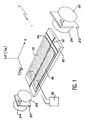
- FIG. 1 schematically represents a component according to the invention.
- This component 1 comprises a parallelepipedic substrate 10 of birefringent material, on which a light guide 12 is formed.
- the substrate 10 has for example a thickness of 0.5 mm, a length of a few tens of mm and a width of 8 mm.
- the guide is produced by diffusion of a metal in the birefringent material.
- This metal is advantageously chosen from titanium (Ti), magnesium (Mg), nickel (Ni), vanadium (Vn) or other materials.
- the guide 12 covers the length of the substrate 10 and has for example a width of 3 micrometers.
- the birefringent material is advantageously chosen from lithium niobate (LiNbO3), lithium tantalate (LiTaO3) or other materials. This material is cut so that an electromagnetic wave propagating in the guide decomposes into two waves having polarizations perpendicular to each other and along the neutral axes of the material.
- the birefringent material being LiNbO3
- the neutral axis corresponding to the extraordinary index is oriented along a Z axis
- the neutral axis corresponding to the ordinary index no is oriented along a Y axis
- the propagation of light in the guide takes place along an X axis.
- the X, Y, Z axes form a space reference.
- the face of the substrate 10 on which the guide 12 is formed is covered with a thin dielectric layer 14, for example SiO having a thickness of approximately 400 nm.
- the dielectric layer 14 is covered by two electrodes 15, 16 for example of aluminum and having a thickness of approximately 500 nm. These electrodes are advantageously rectangular and have a length of 20 mm for example.
- the electrode 15 is arranged so as to cover the guide 12 along its length.
- the guide 12 dividing the face of the substrate 10 into two parts, the electrode 15 largely covers one of the parts and projects beyond the other by about 6 micrometers.
- the other electrode 16 covers another part of the substrate: the difference between the electrodes is for example 7 micrometers.
- the electrodes 15, 16 are connected to an electrical power source 18.
- the assembly formed by the dielectric layer 14, the electrodes 15, 16 and the power source 18, makes it possible to apply an electric field in the substrate 10 , perpendicular to the guide 12 and uniformly along the guide 12.
- the voltages delivered by the power source 18 are of the order of ten volts.
- Component 1 also includes first and second rectilinear polarizers 20, 22 arranged at each end of the light guide 12. These polarizers 20, 22 have polarization directions d1 and d2 parallel and advantageously arranged at 45 ° from the axes Y and Z , that is to say at 45 ° from the neutral axes of the birefringent material, (d1 and d2 are symbolized by arrows in FIG. 1).
- Component 1 further comprises focusing means 24, 26, 28, 30 which allow the polarizers to pass through and a suitable focusing either when the light is introduced into the guide 12 or when it is introduced into an output fiber (not shown).
- the polarizers 20, 22 and the focusing assembly 24, 26, 28, 30 can also be produced by optical fibers.
- Any light beam of any polarization penetrating into the component 1 is firstly polarized rectilinearly and focused in the light guide 12. During its propagation in the guide 12, in the absence of any applied electric field, the wave electromagnetic is divided into two polarization waves directed along the neutral axes of the birefringent material and propagating at different speeds.
- the application of an electric field makes it possible to vary the birefringence of the material and therefore to modify the delay between the two waves.
- the phase shift introduced by the electric field is proportional to its amplitude.
- the two waves are again polarized in parallel.
- the component 1 plays the role of an interferometer.
- FIG. 2 schematically represents a transmission system by coherence modulation comprising a component according to the invention.
- Component 1 plays the role of consistency modulator here.
- the power source 18 allows the application of a variable electric field introducing variations in the delay between the two waves propagating in the light guide.
- the power source 18 may consist of a video amplifier connected to a video camera (not shown) and the output voltage of which is proportional to the signal delivered by the camera. The information contained in this signal is transported in the form of a delay by the light beam inside a single-mode optical fiber 36.
- the delay introduced into the birefringent material must be greater than the coherence length L of the light beam. In this way, the waves produced in the modulator from the light beam do not interfere at the output of the modulator.
- a photodiode 40 of the HgCdTe detector type for example, allows the demodulated light beam to be transformed into an electrical signal. This signal is amplified by an amplifier 42 and allows viewing of the images recorded by the video camera.
- a multiplexing system 50 delivers multiplexed signals on a main transmission line 52.
- the multiplexing system 50 combines a serial architecture with a parallel architecture.
- the system 50 consists of a set of light sources 54 and modulators produced by components 1 in accordance with the invention allowing modulation by optical delays of the light signals delivered by the sources 54.
- the light sources 54 can be single-mode or multimode laser diodes, light-emitting diodes or superluminescent diodes or any combination of these different types of sources.
- the modulators 1 introduce optical delays greater than the coherence lengths of the sources; more generally, they are such that no modulation of the output light intensity appears when the optical delay is modulated by the signal to be transmitted.
- the different stages of the system 50 are connected to the inputs of a coupler 56 which is connected to the main transmission line 52.
- Couplers 58 connected to the transmission line derive part of the multiplexed signals to secondary transmission lines 60.
- the output of each coupler 58 is connected to the input of an optical amplifier 62 whose bandwidth is adapted to the signals transmitting.
- Fiber amplifiers with stimulated Raman effect or the like, semiconductor amplifiers or any other amplifier with sufficient bandwidth can be used.
- Couplers 64 connect the secondary transmission lines to distribution channels 66. In a cable distribution system, these channels 66 serve the users. They are connected to detection systems 68 to demultiplex and demodulate the signals transmitted in the distribution channels. Each coupler 64 has, at the output, as many distribution channels 66 as there are users.
- the signals arriving at the input of the detection system are marred by a noise of intensity inherent to the light sources used. Given the information transmitted, coded in the form of a delay and extracted by constructive interference, the noise brought by the source acts as a multiplicative term of the signals.
- the detection system 68 presented in FIG. 3 overcomes the intensity noise generated by the light sources and the optical amplifier 62. It comprises a separator 70 of the signal transmitted on the distribution channel 66 to which he is connected. This signal is therefore divided into a first signal and a second signal. A detector 72 of the photodiode type delivers an electrical signal proportional to the first signal.
- the second signal is transmitted to a demodulation means 74: for example, a Mach Zehnder type interferometer tuned to the delay introduced by one of the components 1 of the multiplexing system 50.
- This means 74 is connected to a second detector of the photodiode type 76 delivering an electrical signal proportional to the second demodulated signal.
- a divider 78 divides the signal delivered from the second detector 76 by the signal delivered by the first detector 72. At the output of the divider 78, a demodulated signal free of noise due to the light sources 54 and to the optical amplifier 62 is obtained.
- the component according to the invention also performs the function of integrated tunable selective filter.
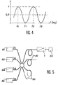
- FIG. 4 schematically represents the transmission curve of a component according to the invention as a function of the frequency of the light wave guided inside the component.
- the transmission T of the component then has the appearance of a sinusoid as a function of the frequency of the light beam. Interference is constructive for frequencies f o , f2, ... and T is 1, whereas they are destructive for the frequencies f1, f3, ... and T is 0.
- the values of f o , f1, ... depend on the characteristics of the component (birefringent material used, length of the guide, value of the applied voltage ).
- the component is therefore in this case a selective filter.
- the value of these frequencies depends on the electric field applied: the filter is tunable.
- FIG. 5 schematically represents a wavelength multiplexing and demultiplexing system comprising the component according to the invention.
- the light sources 80, 82, 84, 86 emit light beams at different wavelengths, ⁇ 1, ⁇ 2, ⁇ 3, ⁇ 4, respectively. These light beams are delivered to the inputs of a coupler 88 which performs their multiplexing and which delivers the multiplexed beams on transmission optical fibers 90.
- the latter are connected to demultiplexing systems comprising a component 1 according to the invention and a photodetector 92.
- the light beams at wavelengths ⁇ 1, ⁇ 2, ⁇ 3, ⁇ 4 have coherence lengths greater than the delay introduced by component 1 which here acts as a tunable selective filter. Indeed, according to the applied electric field, one can choose the wavelength which is transmitted by the component and, filter the others. In order to improve the selectivity of such a device, several components can be connected in series, the transmissions T are all centered on the same wavelength, but the periodicity of the transmission curve is double, triple, ... that of the first component.
Landscapes
- Physics & Mathematics (AREA)
- Nonlinear Science (AREA)
- Chemical & Material Sciences (AREA)
- Engineering & Computer Science (AREA)
- Ceramic Engineering (AREA)
- Crystallography & Structural Chemistry (AREA)
- General Physics & Mathematics (AREA)
- Optics & Photonics (AREA)
- Optical Communication System (AREA)
- Optical Integrated Circuits (AREA)
- Light Guides In General And Applications Therefor (AREA)
Claims (10)
- Mehrzweckbauteil mit integrierter Optik umfassend :- ein Substrat (10) aus doppelbrechendem Material mit zwei neutralen, zueinander senkrecht liegenden Achsen, wobei eine der neutralen Achsen der normalen Indexziffer des Substrats und die andere neutrale Achse der extraordinären Indexziffer des Substrats entspricht,- eine Lichtführung (12), die in einer Seite des Substrats (10) ausgebildet ist,- Einrichtungen (14, 15, 16, 18) zum Anlegen eines elektrischen Feldes,- einen ersten geradlinigen Polarisator (20) der an einem Ende der Lichtführung (12) angeordnet ist,- einen zweiten geradlinigen Polarisator (22), der an dem anderen Ende der Führung (12) angeordnet ist und eine Polarisationsrichtung (d2) aufweist, die zu der (d1) des ersten Polarisators parallel verläuft,- Fokussiermittel (24, 26, 28, 30),dadurch gekennzeichnet, daß :- die Lichtführung (12) zu einer Ebene, die die beiden neutralen Achsen enthält senkrecht steht,- und das angelegte elektrische Feld ist zu der Substratseite (10), in der die Führung (12) ausgebildet ist, senkrecht und entlang der Lichtführung (12) einheitlich.
- Bauteil nach Anspruch 1, dadurch gekennzeichnet, daß das elektrische Feld zumindest eine variable Komponente umfaßt.
- Bauteil nach Anspruch 1, dadurch gekennzeichnet, daß das elektrische Feld zumindest eine kontinuierliche Komponente umfaßt.
- Bauteil nach Anspruch 1, dadurch gekennzeichnet, daß die Mittel (14, 15, 16, 18) zum Anlegen eines elektrischen Feldes umfassen :- eine dielektrische Schicht (14), die die Seite des doppelbrechenden Materials überdeckt, in der die Führung (12) ausgebildet ist ;- eine erste Elektrode (15), die die dielektrische Schicht (14) partiell zumindest über der Lichtführung (12) abdeckt ;- eine zweite Elektrode (16), die einen anderen Teil der dielektrischen Schicht (14) abdeckt ;- eine elektrische Versorgungsquelle (18), die an die Elektroden (15, 16) angeschlossen ist.
- Bauteil nach Anspruch 1, dadurch gekennzeichnet, daß die Polarisationsrichtung (d1, d2) der geradlinigen Polarisatoren (20, 22) in 45 zu neutralen Achsen des doppelbrechenden Materials (10) stehen.
- Bauteil nach Anspruch 1, dadurch gekennzeichnet, daß es einen abstimmbaren optischen Filter darstellt, der eine Ausführung von optischen Demultiplexierfunktionen per Trennung der optischen Frequenzen ermöglicht.
- Verteilungsnetz, dadurch gekennzeichnet, daß es umfaßt :- ein Multiplexiersystem (50), das optische Retardationen auslöst und mehrere Bauteile (1) nach Anspruch 1 umfaßt, um diese Retardationen zu erzeugen ;- eine Hauptübertragungsleitung (52), die mit dem Multiplexiersystem (50) verbunden ist ;- zumindest einen Koppler (58), der die Hauptübertragungsleitung (52) mit sekundären Übertragunsleitungen (60) verbindet ;- zumindest einen optischen Verstärker (62), der es ermöglicht, das optische Leistungsniveau auf eine sekundäre Übertragungsleitung (60) anzuheben.
- Verteilungsnetz nach Anspruch 7, dadurch gekennzeichnet, daß es ferner umfaßt :
- Koppler (64), die die sekundären Übertragungleitungen (60) mit Verteilungswegen (66) verbinden, wobei jeder Verteilungsweg (66) ein Erfassungssystem (68) aufweist, das geeignete Retardationen einführt. - Verteilungsnetz nach Anspruch 8, dadurch gekennzeichnet, daß die Erfassungssysteme (68) jeweils umfassen :- einen Trenner (70) des auf dem Verteilungsweg (66) übermittelten Signals in ein erstes Signal und ein zweites Signal ; und- eine Einrichtung zur Reduktion des Geräuschpegels.
- Verteilungsnetz nach Anspruch 9, dadurch gekennzeichnet, daß die Einrichtung zur Reduktion des Geräuschpegels umfaßt :- eine erste Erfassungseinrichtung (72), die dem ersten Signal ein proportionelles elektrisches Signal übermittelt ;- eine Einrichtung (74) zur Demodulation des zweiten Signals ;- eine zweite Erfassungseinrichtung (76), die dem zweiten demodulierten Signal ein proportionelles Signal übermittelt ;- eine Teilvorrichtung (78), die die Teilung des von der zweiten Erfassungsvorrichtung (72) übermittelten Signals durch das von der ersten Erfassungsvorrichtung (76) übermittelte Signal ausführt.
Applications Claiming Priority (2)
| Application Number | Priority Date | Filing Date | Title |
|---|---|---|---|
| FR8913105A FR2652916B1 (fr) | 1989-10-06 | 1989-10-06 | Composant polyvalent d'optique integree et reseau de distribution avec amplification optique. |
| FR8913105 | 1989-10-06 |
Publications (2)
| Publication Number | Publication Date |
|---|---|
| EP0421880A1 EP0421880A1 (de) | 1991-04-10 |
| EP0421880B1 true EP0421880B1 (de) | 1994-12-28 |
Family
ID=9386173
Family Applications (1)
| Application Number | Title | Priority Date | Filing Date |
|---|---|---|---|
| EP90402751A Expired - Lifetime EP0421880B1 (de) | 1989-10-06 | 1990-10-04 | Polyvalentes integriertes optisches Bauteil und Verteilungsnetz mit optischer Verstärkung |
Country Status (6)
| Country | Link |
|---|---|
| US (1) | US5125049A (de) |
| EP (1) | EP0421880B1 (de) |
| JP (1) | JPH03132620A (de) |
| CA (1) | CA2027036A1 (de) |
| DE (1) | DE69015546T2 (de) |
| FR (1) | FR2652916B1 (de) |
Families Citing this family (3)
| Publication number | Priority date | Publication date | Assignee | Title |
|---|---|---|---|---|
| JPH02289821A (ja) * | 1989-02-17 | 1990-11-29 | Nippon Telegr & Teleph Corp <Ntt> | 光制御素子 |
| FR2673057B1 (fr) * | 1991-02-20 | 1994-04-08 | France Telecom | Reseau de communication optique. |
| WO2018155294A1 (ja) * | 2017-02-22 | 2018-08-30 | シャープ株式会社 | 照明装置および表示装置 |
Family Cites Families (9)
| Publication number | Priority date | Publication date | Assignee | Title |
|---|---|---|---|---|
| US3923374A (en) * | 1974-07-22 | 1975-12-02 | Us Navy | High speed electro-optic waveguide modulator |
| US3951513A (en) * | 1974-09-09 | 1976-04-20 | Masi James V | Semiconductor light modulating optical wave guide |
| CA1236883A (en) * | 1984-07-02 | 1988-05-17 | Neal S. Bergano | Lightwave transmission system using homodyne detection |
| GB2165115B (en) * | 1984-08-25 | 1988-06-02 | Plessey Co Plc | Improvements relating to optical data transmission systems |
| US4614408A (en) * | 1984-08-27 | 1986-09-30 | Eastman Kodak Company | Electrooptic device for scanning and information modulating a plurality of light beams |
| US4691984A (en) * | 1985-09-26 | 1987-09-08 | Trw Inc. | Wavelength-independent polarization converter |
| FR2608869B1 (fr) * | 1986-12-23 | 1988-12-23 | Goedgebuer Jean Pierre | Systeme de multiplexage et de demultiplexage faisant intervenir des retards optiques, pour la transmission de signaux sur fibre optique |
| US4966730A (en) * | 1988-02-11 | 1990-10-30 | E. I. Du Pont De Nemours And Company | Nonlinear optical devices from derivatives of stilbene and diphenylacetylene |
| US4957362A (en) * | 1989-09-08 | 1990-09-18 | Environmental Research Institute Of Michigan | Method and apparatus for electro-optical phase detection |
-
1989
- 1989-10-06 FR FR8913105A patent/FR2652916B1/fr not_active Expired - Fee Related
-
1990
- 1990-10-04 DE DE69015546T patent/DE69015546T2/de not_active Expired - Fee Related
- 1990-10-04 EP EP90402751A patent/EP0421880B1/de not_active Expired - Lifetime
- 1990-10-05 JP JP2268262A patent/JPH03132620A/ja active Pending
- 1990-10-05 US US07/593,090 patent/US5125049A/en not_active Expired - Fee Related
- 1990-10-05 CA CA002027036A patent/CA2027036A1/en not_active Abandoned
Also Published As
| Publication number | Publication date |
|---|---|
| CA2027036A1 (en) | 1991-04-07 |
| DE69015546T2 (de) | 1995-08-17 |
| DE69015546D1 (de) | 1995-02-09 |
| FR2652916B1 (fr) | 1993-10-08 |
| EP0421880A1 (de) | 1991-04-10 |
| US5125049A (en) | 1992-06-23 |
| JPH03132620A (ja) | 1991-06-06 |
| FR2652916A1 (fr) | 1991-04-12 |
Similar Documents
| Publication | Publication Date | Title |
|---|---|---|
| EP0017571B1 (de) | Lichtintensitätsmodulator in integrierter Optik und integrierte optische Schaltung mit einem solchen Modulator | |
| EP0882251B1 (de) | Lichtimpulskontrolle mittels programmierbarer akustooptischer vorrichtung | |
| JP6661913B2 (ja) | 光モジュール、及びこれを用いた光送信機 | |
| FR2502353A1 (fr) | Filtre de longueur d'onde accordable et independant de la polarisation | |
| FR2704702A1 (fr) | Dispositif et procédé de compenssation de dispersion dans un sysstème de transmission à fibre optique. | |
| FR2694817A1 (fr) | Filtre optique accordable interférométrique. | |
| EP0788016A1 (de) | Polarisationsunabhängiger Kerr-Modulator, und nein optischer Taktregenerationsschaltung mit einem derartigen Modulator | |
| FR2772150A1 (fr) | Modulateur optique utilisant un isolateur et transmetteur optique comprenant le susdit | |
| EP0732782A1 (de) | Optischer Duplexer | |
| EP3672109A1 (de) | Vorrichtung und system zur kohärenten rekombination von optischen fasern mit mehreren wellenlängen | |
| FR2796164A1 (fr) | Filtre optique a fibre a reseau de bragg avec une reponse temps de groupe constante dans la bande utile | |
| EP0716486B1 (de) | Wellenlängenkonverter | |
| WO2001098821A1 (fr) | Dispositif acousto-optique programmable | |
| EP0816896B1 (de) | Optisches Bauelement | |
| EP0421880B1 (de) | Polyvalentes integriertes optisches Bauteil und Verteilungsnetz mit optischer Verstärkung | |
| EP0505235A1 (de) | Breitbandinterkorrelationsverfahren und Vorrichtung | |
| EP0099282A1 (de) | Von der Polarisation unabhängiger integriert-optischer Modulator | |
| CA2292789A1 (fr) | Modulateur de type mach-zehnder presentant un taux d'extinction tres eleve | |
| FR2728357A1 (fr) | Dispositif acousto-optique pour filtrage optique | |
| EP3200363B1 (de) | System zur linearen optischen abtastung und kohärenten erkennung eines optischen signals | |
| EP0671791A1 (de) | Elektrooptischer Halbleitermodulator und optisches Transmissionssystem unter Verwendung dieses Modulators | |
| FR3025659A1 (fr) | Source laser multi-longueurs d'onde auto-alignee et emetteur-recepteur integrant une telle source | |
| FR2746192A1 (fr) | Dispositif optique non-lineaire de traitement de signaux optiques | |
| FR2685786A1 (fr) | Coupleur de proximite en optique integree. | |
| EP0849620B1 (de) | Elektrooptischer Lichtmodulator |
Legal Events
| Date | Code | Title | Description |
|---|---|---|---|
| PUAI | Public reference made under article 153(3) epc to a published international application that has entered the european phase |
Free format text: ORIGINAL CODE: 0009012 |
|
| AK | Designated contracting states |
Kind code of ref document: A1 Designated state(s): DE GB NL |
|
| 17P | Request for examination filed |
Effective date: 19910914 |
|
| 17Q | First examination report despatched |
Effective date: 19931012 |
|
| RAP1 | Party data changed (applicant data changed or rights of an application transferred) |
Owner name: FRANCE TELECOM |
|
| GRAA | (expected) grant |
Free format text: ORIGINAL CODE: 0009210 |
|
| AK | Designated contracting states |
Kind code of ref document: B1 Designated state(s): DE GB NL |
|
| REF | Corresponds to: |
Ref document number: 69015546 Country of ref document: DE Date of ref document: 19950209 |
|
| GBT | Gb: translation of ep patent filed (gb section 77(6)(a)/1977) |
Effective date: 19950301 |
|
| PLBE | No opposition filed within time limit |
Free format text: ORIGINAL CODE: 0009261 |
|
| STAA | Information on the status of an ep patent application or granted ep patent |
Free format text: STATUS: NO OPPOSITION FILED WITHIN TIME LIMIT |
|
| 26N | No opposition filed | ||
| PGFP | Annual fee paid to national office [announced via postgrant information from national office to epo] |
Ref country code: GB Payment date: 19960927 Year of fee payment: 7 |
|
| PGFP | Annual fee paid to national office [announced via postgrant information from national office to epo] |
Ref country code: DE Payment date: 19961022 Year of fee payment: 7 |
|
| PGFP | Annual fee paid to national office [announced via postgrant information from national office to epo] |
Ref country code: NL Payment date: 19961031 Year of fee payment: 7 |
|
| PG25 | Lapsed in a contracting state [announced via postgrant information from national office to epo] |
Ref country code: GB Free format text: LAPSE BECAUSE OF NON-PAYMENT OF DUE FEES Effective date: 19971004 |
|
| PG25 | Lapsed in a contracting state [announced via postgrant information from national office to epo] |
Ref country code: NL Free format text: LAPSE BECAUSE OF NON-PAYMENT OF DUE FEES Effective date: 19980501 |
|
| GBPC | Gb: european patent ceased through non-payment of renewal fee |
Effective date: 19971004 |
|
| NLV4 | Nl: lapsed or anulled due to non-payment of the annual fee |
Effective date: 19980501 |
|
| PG25 | Lapsed in a contracting state [announced via postgrant information from national office to epo] |
Ref country code: DE Free format text: LAPSE BECAUSE OF NON-PAYMENT OF DUE FEES Effective date: 19980701 |