EP0422541A2 - Méthode et appareil pour affichage parallèle de polygones et de pixels - Google Patents
Méthode et appareil pour affichage parallèle de polygones et de pixels Download PDFInfo
- Publication number
- EP0422541A2 EP0422541A2 EP90119223A EP90119223A EP0422541A2 EP 0422541 A2 EP0422541 A2 EP 0422541A2 EP 90119223 A EP90119223 A EP 90119223A EP 90119223 A EP90119223 A EP 90119223A EP 0422541 A2 EP0422541 A2 EP 0422541A2
- Authority
- EP
- European Patent Office
- Prior art keywords
- edge
- interpolator
- memory
- polygon
- raster engine
- Prior art date
- Legal status (The legal status is an assumption and is not a legal conclusion. Google has not performed a legal analysis and makes no representation as to the accuracy of the status listed.)
- Granted
Links
Images


Classifications
-
- G—PHYSICS
- G06—COMPUTING OR CALCULATING; COUNTING
- G06T—IMAGE DATA PROCESSING OR GENERATION, IN GENERAL
- G06T15/00—Three-dimensional [3D] image rendering
- G06T15/50—Lighting effects
- G06T15/80—Shading
- G06T15/87—Gouraud shading
Definitions
- This invention is directed generally to a rendering engine architecture for computer graphics and, more specifically, to a parallel polygon/pixel rendering engine and method for providing three-dimensional Gouraud shaded objects rapidly.
- Known polygon raster engines typically rasterize only one polygon at a time, a single line at a time while using only one rendering engine pipeline.
- the invention offers an improvement over the prior art by providing an apparatus which rasterizes one polygon at a time by simultaneously creating multiple lines of pixels to rapidly fill the polygon.
- the simultaneous rendering of multiple lines results in an increase in throughput capability which further enables display animation to be achieved.
- EP-A 0 382 139 entitled Generic Interpolation Pipeline Processor published 16.08.1990, and EP-A 0 379 983 entitled "Memory Interface Controller” published 01.08.1990 are incorporated herein by reference in their entirety.
- EP-A 0 382 139 teaches a generic interpolation pipeline processor or "GIPP" design to accelerate the polygon draw-and-fill operations used in real-time video display systems.
- the GIPP performs integer interpolation calculations, such as those found in intensity interpolation shading, at high speed (effectively, for example, 225 million operations per second).
- a single independent variable is used to calculate two different dependent variables in parallel.
- a single GIPP can be used to draw correctly shaded monochrome lines at up to 25 million pixels per second.
- the GIPP is equipped with an internal counter to allow the drawing of shaded lines by specifying only the values at the end points.
- the inputs are double-buffered to allow efficient utilization of the chip's speed.
- the GIPP uses hardware handshaking to read its input data, and supply status bits indicating division by zero or invalid output data.
- Two GIPPs may be used to draw polygon edges and another one or more may be used to fill between the edges with a minimal amount of extraneous logic. When polygon edges are joined at their end points, a Join signal may be used to avoid writing both new end points into the GIPP.
- the present invention utilizes a plurality of GIPPs in order to accomplish high speed rendering of graphic display objects.
- the memory interface controller (MIC) of EP-A 0 379 983 is a memory interface controller apparatus for use in a digital system, such as a graphics display system.
- the apparatus comprises means for initializing the system memory, means for receiving incoming pixel data and means for performing hidden surface removal on the incoming pixel data as well as means for construction of images with transparent objects.
- the present invention uses a plurality of MICs in combination with GIPPs as well as other elements in order to provide three-dimensional animation with Gouraud shading.
- the apparatus of the invention provides a raster graphics generator (RGG) including a parallel polygon/pixel rendering engine for a digital map capable of producing real-time linear shaded, three dimensional, raster graphics for video generation.
- RMG raster graphics generator
- the invention is suitable for use with avionic display systems, particularly digital map displays which include an instruction and interpreter unit and an image scanner.
- the apparatus of the invention as characterized in claim 1 comprises a raster engine, a memory interface and a bit mapped memory.
- the raster engine further includes a raster engine control and generic interpolation polygon processsor interface, an edge interpolator, a line interpolator and a controller for the edge and line interpolators.
- the raster engine control and GIPP interface is electrically connected to receive data from the instruction interface unit and is further electrically connected to the edge interpolator and interpolator controller.
- the edge interpolator is adapted to receive data from the raster engine control and the line interpolator is electrically connected to receive data from the edge interpolator.
- a first edge pipeline is connected to a second output of the raster engineer control and GIPP interface and a second edge pipeline is connected to an output of the first edge pipeline as well as an output of the edge interpolator.
- An output from the second stage of the edge pipeline and a plurality of outputs from the line interpolators are then fed to a memory interface which is connected to receive data from the plurality of outputs.
- the memory interface accepts color, linearly shaded, three dimensional pixel data from the raster edge.
- the memory interface controls data transfers between the raster engine and the memory interface with a hold control signal.
- a bit mapped memory controller is connected to the memory interface.
- a bit mapped memory is also connected to receive data from the memory interface and control signals from the bit mapped memory controller.
- the bit map memory controller controls the memory interface components and the bit map memory during both normal and test modes.
- the edge interpolator is comprised of a plurality of generic interpolation pipeline processors or GIPPs.
- the edge interpolators may preferably comprise at least two GIPPs while the line interpolators may preferably comprise at least four GIPPs.
- the memory interface is preferably comprised of a plurality of memory interface chips (MICs).
- the bit mapped memory controller is preferably comprised of programmable logic arrays.
- a plurality of test interface units may be included in the design of the raster engine in order to facilitate manufacturing and debugging procedures should a failure occur.
- the raster engine of the invention has the capability for simultaneously rendering multiple polygon lines for a single polygon.
- the raster engine uses an interleaved memory wherein each parallel pipeline works with a portion of the memory. Such raster engine for a digital display system significantly increases throughput of data for rendering images.
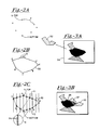
- FIGs 2A, 2B, 2C sequentially illustrate the computer algorithm employed by the invention to generate polygons used for rapidly providing three dimensional Gouraud shaded objects.
- the raster engine initially accepts data representing a number of points a, b, c, d, e, f and g, generally designated P. Each point is described by cartesian coordinates (X, Y, Z), color coordinates (R, G, B), a translucency coefficient (K) and an invisibility factor (T).
- the points, P are sorted from top to bottom using the Y coordinate as the sorting discriminator.
- the points generally define a convex polygon.
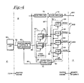
- Figure 1 shows a block diagram of one embodiment of the polygon/pixel rendering engine of the invention is shown as used in a display system including an instruction interpreter unit (IIU) 10 and an image scanner 18.
- the raster graphics generator 100 of the invention comprises a raster engine 12, a memory interface 14, and a bit mapped memory 16 having a controller 20.
- the invention may advantageously include test interfaces 40, 42 and 44.
- the instruction interpreter unit 10 (IIU) provides an interface for the command bus 46, accepts and processes the graphics commands as provided by the display system 50, and outputs polygon commands to the raster engine via bus 52.
- the raster engine 12 receives polygon commands via bus 52 from the IIU and outputs linearly shaded, color raster graphics video to the memory interface via bus 54.
- the memory interface is connected to receive the raster graphics video signals from the raster engine via bus 54.
- the memory interface also implements hidden surface removal and transparency processes as required for the polygons rendered by the raster engine.
- the memory interface also outputs this processed data to the bit mapped memory 16.
- the bit mapped memory (BMM) 16 has two purposes. It is used by the memory interface as a read/write frame buffer to perform transparency and hidden surface removal processes, and it interfaces with the video bus 56, providing colored, transparent, linearly shaded, three dimensional raster graphics video signals to the image scanner 18 via video bus 56.
- the controller 20 provides control signals to the memory interface and BMM during both normal and test modes.
- test interface units 40 and 42 and test interface controller 44 may be advantageously included in a system utilizing the apparatus of the invention for facilitating manufacturing and debugging of large scale integrated circuits embodying the apparatus of the invention. In some cases it may be preferable to build the system as an application specific integrated circuit (ASIC) from gallium arsenide semi-conductor material.
- ASIC application specific integrated circuit
- Figures 3A and 3B conceptually illustrate the addition of a polygon 32 to a bit mapped memory 34 already containing several rendered polygons.
- the polygon 32 in this example, exhibits transparency characteristics as can be shown in Figure 2B since the polygon 36 has an area 37 which is visible through the overlaid polygon 32 which is overlaid on polygon 36.
- several polygons are typically joined in this fashion to create images and symbols representing objects in the real world such as terrain, trees, vehicles, etc.
- the IIU 10 further includes a vertex list 60.
- the raster engine 12 is further comprised of the raster engine control and GIPP interface 62, edge interpolator 64, line interpolators 68, a first stage edge pipeline 70 and a second stage edge pipeline 72.
- the raster engine control and GIPP interface (REC) 62 is advantageously implemented in a programmable logic device. The REC reads data transmitted on bus 52 from the vertex list 60 which is typically comprised of an instruction list RAM further including at least two.
- the REC reads the data from the instruction list RAM on an as needed basis to provide data line 80 as required by the edge interpolators 64. Serving as a controller between the edge interpolators and the line interpolators is inter-GIPP controller 74. The REC is further explained below with reference to the REC diagram shown in Figure 8.
- the edge interpolators 64 are preferably comprised of a first and second edge interpolators GIPP1 and GIPP2 which are each further comprised of at least three GIPP chips.
- Each GIPP chip can interpolate two axes at a time across the coordinate. Therefore, six of these chips are used for the edge interpolation function.
- Each of the chips provides edge data, in this case along the X axis to the second stage of the edge pipeline 72 via bus 82.
- there are four line interpolators 84 each comprised of at least 2 GIPP chips.
- Each line interpolator 84 linearly interpolates Z, R, G and B across the Y coordinates.
- the line interpolators have outputs 86B which feed the interpolated data into the memory interface 14.
- the inter-GIPP controller 74 is electrically connected between the edge and line interpolators.
- the inter-GIPP controller coordinates the transfer of data between the edge interpolators and the line interpolators and monitors the operation of the edge interpolation GIPP chips. Processing of pixel data interior to the polygons is evenly distributed among the four line interpolators by decoding the two least significant bits, (LSBs) of each pixel's X coordinate as the data is clocked out of the edge interpolator onto an inter-GIPP bus 88. Since both edge interpolators share bus 88, the inter-GIPP controller 74 also includes a multiplexer for multiplexing the data by controlling the output enables of the GIPPs via control lines 90 and 92.
- LSBs least significant bits
- the inter-GIPP controller further monitors the same two bits of each X coordinate from each of the two edge interpolators 76 to ensure that the data is synchronized as it is passed to the line interpolators. If an error is detected in this synchronization check, error recovery is handed off to the REC 80 through a discrete output 94.
- the REC reads from two instruction lists which are contained in the vertex list 60.
- the first instruction list corresponds to information required for the first edge interpolator GIPP1 and the second corresponds to information required for edge interpolator GIPP2.
- Each new vertex is JOIN loaded to the last point in accordance with the JOIN function of the GIPP chips as described in Miller, et al.
- End of file (EOF) and end of polygon (EOP) comprise data in the form of "TAGS" stored in the vertex list 60.
- the raster engine controller waits for a frame synchronization signal prior to resetting the edge interpolator GIPPS at step 222. After resetting the edge interpolator GIPPS at step 222, the first edge of the polygon is loaded to both edge interpolators at step 224. The raster engine controller will not overload the GIPPS, therefore, at steps 226 and 228.
- the polygon abcdefg of Figure 2B may be divided into two display lists.
- the first display list would include vertices a, b, c and d and the second display list would include vertices a, g, f, e and d.
- the raster engine controller would read the first display list into the first set of edge GIPPs and the second display list into the second set of edge GIPPS.
- point d would be tagged with an end of polygon signal 1 (EOP1) to signify the end of the first display list to the raster engine controller.
- EOP1 end of polygon signal 1
- EOP2 end of polygon 2
- the first display list will signal end of polygon prior to exhausting the second display list.
- the end of polygon signals EOP1 and EOP2 do not refer to separate polygons but two separate display lists describing the top and bottom of a single polygon.
- the polygon could have been divided from left to right using the top most and bottom most values, namely b and f, as the beginning and end of the polygon markers.
- the point d is tagged once with a single bit to denote end of polygon.
- the controller recognizes the end of display list 1 or display list 2 as the case may be, through correlation with the time at which the signal is received.
- the raster engine controller therefore, proceeds to process the polygon edges at steps 226 and 228.
- step 226 if the first set of edge GIPPs is not full it loads the mix points from display list 1, if the display list is not exhausted, it proceeds to load edge GIPP2 with the next points from display list 2 at step 228. If step 228 encounters an EOP2 signal the process proceeds to step 230 which checks to see if the first set of edge GIPPs is full until an EOP1 signal is received signifying the exhaustion of the display list for edge GIPP1.
- step 226 encounters an EOP1 signal, the raster engine controller proceeds to finish filling the set of second edge GIPPs until an EOF or EOP2 signal is received.
- An EOF signal signifies the exhaustion of all polygons in the construction list memory and returns control to step 220 to await the next frame signal.
- both edge GIPP interpolators interpolate the edges from left to right with the first edge interpolator, interpolating the top most points and the second edge interpolator interpolating the bottom most points.
- the information is passed to the line interpolators which interpolate in a similar manner across the Y coordinates of the system as explained with reference with Figure 2C above.
- the memory interface as implement in one embodiment of the invention comprises at least 4 MIC chips 102.
- the interface lines shown are consistent with those described by Snodgrass, et al.
- the memory interface 14 accepts color, linearly shaded, three dimensional pixel data from the raster engine 12.
- the memory interface controls data transfers between the raster engine and the memory interface with the holds control line signals. HOLD 1, HOLD 2, HOLD 3 and HOLD 4.
- FIG. 6 a more detailed block diagram of a portion of the bit mapped memory is shown with the interfaces between the bit mapped memory and the memory interface and the bit mapped memory and the video bus.
- the portion shown in Figure 6 is one of four identical sections of the bit mapped memory.
- the memory interface reads pixel data from the BMM which is located at the same screen coordinates as the pixel data received from the raster engine.
- the memory interface performs hidden surface removal by comparing the Z-coordinates of the corresponding pixels.
- the pixel that is "in front" of the other i.e., the pixel occupying a place on the display screen which is closer to the front of the screen
- the new pixel is written into the BMM by the memory interface.
- the memory interface performs self-test or BMM test at the command of the IIU.
- the memory interface is also responsible for clearing the BMM before processing the next display's information.
- the color, Z-coordinate, and transparency initial settings are configured by the IIU in a well-known manner.
- the memory interface operates at 12.5 MHz for processing data and 25 MHz for memory accesses.
- the memory interface processes a maximum of 50 million pixels per second.
- the BMM provides the memory interface with a frame buffer which is used by the memory interface as a read-modify-write module to perform hidden surface removal and transparency functions.
- the BMM is shown in Figure 6 as comprised of a PING-PONG frame buffer memory including PING registers 104 and 106 and RAM 108, as well as output buffer 110.
- the PONG section of the memory comprises registers 112, 114 and RAM 116 together with output buffer 118.
- a third section comprises a Z buffer including registers 120, 122 and RAM 124.
- the BMM also provides a video bus interface for the rendering engine. A space is provided for color values and transparency factors. At any given time, one half of the memory is used by the memory interface and the other half by the video bus.
- the BMM memory is frame sized and provides space for Z-coordinates. The BMM operates in a pipe-line fashion for the memory interface and an asynchronous fashion for the video bus.
- the memory interface 14 to BMM 16 interface is comprised of a bi-directional data bus and memory controlled discrete lines.
- the memory interface 14 reads or writes pixel data in 25 MHz cycles.
- the pixel data is defined by its address (screen coordinates (X, Y)), its Z-depth, its color (R, G, B) and its transparency factor (K).
- the coordinate system is right handed with the origin at the upper left hand corner of the view volume.
- the memory interface outputs four control signals to the BMM: WRITE-EN*, CLK-EN*, READ*, and WRITE*. These signals are described in EP-A 0 379 983.
- the BMM controller 20 is preferably implemented in a programmable array logic device (PAL).
- PAL programmable array logic device
- the BMM controller interfaces the raster graphics generator with the image scanner 18 and provides control signals to the MIC within the memory interface. It also provides control signals to the BMM during both normal operational and test modes.
- FIG. 7B shows a flow chart diagram of an initialization method processed by the BMM controller in the preferred embodiment of the invention.
- the BMM controller 20 waits for an end of frame (EOF*) signal from the raster engine. When this occurs, it then waits at step 202 for all the empty signals (EMPTY0*, EMPTY1*, EMPTY2*, and EMPTY3*) on all four MIC chips to go low. This event indicates that all the pipeline is empty.
- the BMM controller asserts a signal called RGG_COMPLETE* to the image scanner. This signal is applied when the raster graphics generator has finished processing all the information for the display in a predetermined allotted time frame.
- the video bus controls the PING-PONG function of the BMM by asserting a signal called FRAME_SYNC*.
- the BMM controller changes the appropriate control signals so as to allow the video bus and the MICs to change which half of the PING-PONG memory they are accessing at step 206.
- the BMM controller determines which half of the memory the MICs can access and which half of the memory the video bus can access.
- the MICs and the video bus work simultaneously on opposite halves.
- the controller asserts a CLEAR* signal at step 210 which is transmitted to the MIC chips. This causes the MICs to initialize the half of memory they are allowed access. CLEAR* is deasserted when the MICs signal the completion of initialization by asserting all the MIC empty bits. Upon completion of the initialization cycles, the MICs and the BMM are ready to process the new image. The cycle repeats itself for each new image.
- the soft reset (S_R*) signal is transmitted from the IIU in some cases. Upon receiving this signal, CLEAR* is asserted which causes the MICs to reset and then clear the BMM.
- test interface signals are also included as inputs to the BMM controller, namely, TEST, MIC/MEM* and PING-PONG*.
- the three test interface signals are only used when the raster graphics generator is in test mode.
- the TEST pin is asserted by the TI during test mode.
- the MIC/MEM* signal is sued to signify that the TI is examining the output of the MICs or interfacing with the BMM. If this signifies the latter, the third pin, PING/PONG* is used to select which half of the BMM is being accessed by the IIU. If the BMM is selected, the controller tri-states the MICs' outputs by asserting an OUTPUT_DIS signal.
Landscapes
- Engineering & Computer Science (AREA)
- Computer Graphics (AREA)
- Physics & Mathematics (AREA)
- General Physics & Mathematics (AREA)
- Theoretical Computer Science (AREA)
- Image Generation (AREA)
Applications Claiming Priority (2)
| Application Number | Priority Date | Filing Date | Title |
|---|---|---|---|
| US41972289A | 1989-10-11 | 1989-10-11 | |
| US419722 | 1989-10-11 |
Publications (3)
| Publication Number | Publication Date |
|---|---|
| EP0422541A2 true EP0422541A2 (fr) | 1991-04-17 |
| EP0422541A3 EP0422541A3 (en) | 1993-01-13 |
| EP0422541B1 EP0422541B1 (fr) | 1997-02-26 |
Family
ID=23663475
Family Applications (1)
| Application Number | Title | Priority Date | Filing Date |
|---|---|---|---|
| EP90119223A Expired - Lifetime EP0422541B1 (fr) | 1989-10-11 | 1990-10-06 | Méthode et appareil pour affichage parallèle de polygones et de pixels |
Country Status (5)
| Country | Link |
|---|---|
| US (1) | US5392392A (fr) |
| EP (1) | EP0422541B1 (fr) |
| JP (2) | JPH03241480A (fr) |
| CA (1) | CA2026527A1 (fr) |
| DE (1) | DE69029987T2 (fr) |
Cited By (6)
| Publication number | Priority date | Publication date | Assignee | Title |
|---|---|---|---|---|
| GB2259432A (en) * | 1991-09-06 | 1993-03-10 | Canon Res Ct Europe Ltd | Three dimensional graphics processing |
| EP0620532A3 (fr) * | 1993-04-15 | 1996-11-06 | Sony Corp | Procédé et dispositif pour la création d'un signal d'image tridimensionnel et de son affichage en deux dimensions. |
| GB2343602A (en) * | 1998-11-06 | 2000-05-10 | Videologic Ltd | Shading 3-dimensional computer generated images |
| WO2001071519A3 (fr) * | 2000-03-23 | 2002-06-06 | Sony Computer Entertainment Inc | Appareil et procede de traitement d'images |
| US6924807B2 (en) | 2000-03-23 | 2005-08-02 | Sony Computer Entertainment Inc. | Image processing apparatus and method |
| CN102831631A (zh) * | 2012-08-23 | 2012-12-19 | 上海创图网络科技发展有限公司 | 一种大规模三维动画的渲染方法及渲染装置 |
Families Citing this family (17)
| Publication number | Priority date | Publication date | Assignee | Title |
|---|---|---|---|---|
| IL102289A (en) * | 1992-06-24 | 1997-08-14 | R Technologies Ltd B V | Method and system for processing moving images |
| US5619624A (en) * | 1994-05-20 | 1997-04-08 | Management Graphics, Inc. | Apparatus for selecting a rasterizer processing order for a plurality of graphic image files |
| KR100243179B1 (ko) * | 1994-06-30 | 2000-02-01 | 윤종용 | 그래픽 시스템의 신호처리방법 및 장치 |
| US5611029A (en) * | 1995-01-31 | 1997-03-11 | Compaq Computer Corporation | Run slice line draw engine with non-linear shading capabilities |
| DE69630261T2 (de) * | 1995-06-30 | 2004-08-05 | Matsushita Electric Industrial Co., Ltd., Kadoma | Verfahren und Vorrichtung zum Darstellen und Abbilden von Bildern |
| US5696944A (en) * | 1995-08-08 | 1997-12-09 | Hewlett-Packard Company | Computer graphics system having double buffered vertex ram with granularity |
| US6434649B1 (en) * | 1998-10-14 | 2002-08-13 | Hitachi, Ltd. | Data streamer |
| US6560674B1 (en) | 1998-10-14 | 2003-05-06 | Hitachi, Ltd. | Data cache system |
| US6347344B1 (en) * | 1998-10-14 | 2002-02-12 | Hitachi, Ltd. | Integrated multimedia system with local processor, data transfer switch, processing modules, fixed functional unit, data streamer, interface unit and multiplexer, all integrated on multimedia processor |
| US6608625B1 (en) | 1998-10-14 | 2003-08-19 | Hitachi, Ltd. | Three dimensional graphic processor |
| US6240341B1 (en) * | 1999-01-18 | 2001-05-29 | Honeywell International Inc. | Flight management system (FMS) with integrated bit mapped data charts |
| KR100385233B1 (ko) * | 2000-03-14 | 2003-05-23 | 삼성전자주식회사 | 데이터 프로세싱 시스템의 익스포넌트 유닛 |
| US6651116B1 (en) | 2000-05-15 | 2003-11-18 | International Business Machines Corporation | Output interface for a raster object memory in a method, system and program |
| US7119809B1 (en) * | 2000-05-15 | 2006-10-10 | S3 Graphics Co., Ltd. | Parallel architecture for graphics primitive decomposition |
| US6831647B1 (en) * | 2000-09-28 | 2004-12-14 | Rockwell Automation Technologies, Inc. | Raster engine with bounded video signature analyzer |
| GB0823254D0 (en) | 2008-12-19 | 2009-01-28 | Imagination Tech Ltd | Multi level display control list in tile based 3D computer graphics system |
| US9721363B2 (en) * | 2014-05-19 | 2017-08-01 | Google Inc. | Encoding polygon data for fast retrieval and rendering |
Family Cites Families (6)
| Publication number | Priority date | Publication date | Assignee | Title |
|---|---|---|---|---|
| US4974177A (en) * | 1985-10-04 | 1990-11-27 | Daikin Industries Ltd. | Mapping circuit of a CRT display device |
| US4924414A (en) * | 1986-09-24 | 1990-05-08 | Daikin Industries, Ltd. | Apparatus and method for obtaining priority numbers for drawing figures forming a display figure |
| JPH0812705B2 (ja) * | 1986-09-29 | 1996-02-07 | 株式会社東芝 | 画像処理装置 |
| US5088053A (en) * | 1987-11-16 | 1992-02-11 | Intel Corporation | Memory controller as for a video signal processor |
| US4949280A (en) * | 1988-05-10 | 1990-08-14 | Battelle Memorial Institute | Parallel processor-based raster graphics system architecture |
| US5060172A (en) * | 1989-07-06 | 1991-10-22 | Digital Equipment Corporation | Method and apparatus for displaying smooth-shaded objects |
-
1990
- 1990-09-28 CA CA002026527A patent/CA2026527A1/fr not_active Abandoned
- 1990-10-06 EP EP90119223A patent/EP0422541B1/fr not_active Expired - Lifetime
- 1990-10-06 DE DE69029987T patent/DE69029987T2/de not_active Expired - Fee Related
- 1990-10-11 JP JP2270662A patent/JPH03241480A/ja active Pending
-
1993
- 1993-01-12 US US08/004,476 patent/US5392392A/en not_active Expired - Lifetime
-
1999
- 1999-10-08 JP JP007679U patent/JP2000000018U/ja active Pending
Cited By (13)
| Publication number | Priority date | Publication date | Assignee | Title |
|---|---|---|---|---|
| US5579454A (en) * | 1991-09-06 | 1996-11-26 | Canon Kabushiki Kaisha | Three dimensional graphics processing with pre-sorting of surface portions |
| GB2259432A (en) * | 1991-09-06 | 1993-03-10 | Canon Res Ct Europe Ltd | Three dimensional graphics processing |
| EP1008958A1 (fr) * | 1993-04-15 | 2000-06-14 | Sony Corporation | Procédé et dispositif pour la création d'un signal d'image tridimensionnelet de son affichage en deux dimensions |
| EP0620532A3 (fr) * | 1993-04-15 | 1996-11-06 | Sony Corp | Procédé et dispositif pour la création d'un signal d'image tridimensionnel et de son affichage en deux dimensions. |
| GB2343602B (en) * | 1998-11-06 | 2003-03-19 | Videologic Ltd | Shading 3-dimensional computer generated images |
| GB2343602A (en) * | 1998-11-06 | 2000-05-10 | Videologic Ltd | Shading 3-dimensional computer generated images |
| US6741247B1 (en) | 1998-11-06 | 2004-05-25 | Imagination Technologies Limited | Shading 3-dimensional computer generated images |
| EP1127337B2 (fr) † | 1998-11-06 | 2014-03-26 | Imagination Technologies Limited | Ombrage d'images informatiques en trois dimensions |
| WO2001071519A3 (fr) * | 2000-03-23 | 2002-06-06 | Sony Computer Entertainment Inc | Appareil et procede de traitement d'images |
| JP2003528394A (ja) * | 2000-03-23 | 2003-09-24 | 株式会社ソニー・コンピュータエンタテインメント | 画像処理装置及び画像処理方法 |
| US6924807B2 (en) | 2000-03-23 | 2005-08-02 | Sony Computer Entertainment Inc. | Image processing apparatus and method |
| CN102831631A (zh) * | 2012-08-23 | 2012-12-19 | 上海创图网络科技发展有限公司 | 一种大规模三维动画的渲染方法及渲染装置 |
| CN102831631B (zh) * | 2012-08-23 | 2015-03-11 | 上海创图网络科技发展有限公司 | 一种大规模三维动画的渲染方法及渲染装置 |
Also Published As
| Publication number | Publication date |
|---|---|
| EP0422541A3 (en) | 1993-01-13 |
| US5392392A (en) | 1995-02-21 |
| DE69029987T2 (de) | 1997-07-24 |
| DE69029987D1 (de) | 1997-04-03 |
| CA2026527A1 (fr) | 1991-04-12 |
| JPH03241480A (ja) | 1991-10-28 |
| JP2000000018U (ja) | 2000-02-18 |
| EP0422541B1 (fr) | 1997-02-26 |
Similar Documents
| Publication | Publication Date | Title |
|---|---|---|
| US5392392A (en) | Parallel polygon/pixel rendering engine | |
| US5553208A (en) | Image synthesizing system having a field buffer unit that stores texture coordinates | |
| US5649173A (en) | Hardware architecture for image generation and manipulation | |
| US4829295A (en) | Image synthesizer | |
| US6456284B1 (en) | Graphics processor, system and method for generating screen pixels in raster order utilizing a single interpolator | |
| US6999087B2 (en) | Dynamically adjusting sample density in a graphics system | |
| US5801711A (en) | Polyline and triangle strip data management techniques for enhancing performance of computer graphics system | |
| US6975322B2 (en) | Dynamically adjusting a number of rendering passes in a graphics system | |
| US7358974B2 (en) | Method and system for minimizing an amount of data needed to test data against subarea boundaries in spatially composited digital video | |
| US5757374A (en) | Method and apparatus for performing texture mapping | |
| EP0367183A2 (fr) | Système de traitement à grande vitesse d'images graphiques informatiques | |
| EP0740272A2 (fr) | Procédé et dispositif pour représenter rapidement une image à trois dimensions | |
| JP2001357410A (ja) | 別々に生成された3次元イメージを合成するグラフィックス・システム | |
| US4845663A (en) | Image processor with free flow pipeline bus | |
| US20030169259A1 (en) | Graphics data synchronization with multiple data paths in a graphics accelerator | |
| US6750869B1 (en) | Method and design for improved fragment processing | |
| EP1345168B1 (fr) | Réglage dynamique de la densité d'échantillonnage et/ou de la fréquence de rendu dans un système graphique | |
| US20030043159A1 (en) | Graphics resampling system and method for use thereof | |
| US5784075A (en) | Memory mapping techniques for enhancing performance of computer graphics system | |
| EP0425187B1 (fr) | Dessin de primitives du type "polygone avec bords" dans un système d'affichage graphique commandé par ordinateur | |
| US5671373A (en) | Data bus protocol for computer graphics system | |
| US5943066A (en) | Programmable retargeter method and apparatus | |
| US5883642A (en) | Programmable retargeter method and apparatus | |
| US6563507B1 (en) | Storage circuit control device and graphic computation device | |
| JPH05249953A (ja) | 画像表示装置 |
Legal Events
| Date | Code | Title | Description |
|---|---|---|---|
| PUAI | Public reference made under article 153(3) epc to a published international application that has entered the european phase |
Free format text: ORIGINAL CODE: 0009012 |
|
| AK | Designated contracting states |
Kind code of ref document: A2 Designated state(s): DE FR GB IT |
|
| PUAL | Search report despatched |
Free format text: ORIGINAL CODE: 0009013 |
|
| AK | Designated contracting states |
Kind code of ref document: A3 Designated state(s): DE FR GB IT |
|
| 17P | Request for examination filed |
Effective date: 19930710 |
|
| 17Q | First examination report despatched |
Effective date: 19951121 |
|
| GRAG | Despatch of communication of intention to grant |
Free format text: ORIGINAL CODE: EPIDOS AGRA |
|
| GRAH | Despatch of communication of intention to grant a patent |
Free format text: ORIGINAL CODE: EPIDOS IGRA |
|
| GRAH | Despatch of communication of intention to grant a patent |
Free format text: ORIGINAL CODE: EPIDOS IGRA |
|
| GRAA | (expected) grant |
Free format text: ORIGINAL CODE: 0009210 |
|
| AK | Designated contracting states |
Kind code of ref document: B1 Designated state(s): DE FR GB IT |
|
| REF | Corresponds to: |
Ref document number: 69029987 Country of ref document: DE Date of ref document: 19970403 |
|
| ET | Fr: translation filed | ||
| ITF | It: translation for a ep patent filed | ||
| PLBE | No opposition filed within time limit |
Free format text: ORIGINAL CODE: 0009261 |
|
| STAA | Information on the status of an ep patent application or granted ep patent |
Free format text: STATUS: NO OPPOSITION FILED WITHIN TIME LIMIT |
|
| 26N | No opposition filed | ||
| PGFP | Annual fee paid to national office [announced via postgrant information from national office to epo] |
Ref country code: GB Payment date: 20010914 Year of fee payment: 12 |
|
| PGFP | Annual fee paid to national office [announced via postgrant information from national office to epo] |
Ref country code: FR Payment date: 20011005 Year of fee payment: 12 |
|
| PGFP | Annual fee paid to national office [announced via postgrant information from national office to epo] |
Ref country code: DE Payment date: 20011030 Year of fee payment: 12 |
|
| REG | Reference to a national code |
Ref country code: GB Ref legal event code: IF02 |
|
| PG25 | Lapsed in a contracting state [announced via postgrant information from national office to epo] |
Ref country code: GB Free format text: LAPSE BECAUSE OF NON-PAYMENT OF DUE FEES Effective date: 20021006 |
|
| PG25 | Lapsed in a contracting state [announced via postgrant information from national office to epo] |
Ref country code: DE Free format text: LAPSE BECAUSE OF NON-PAYMENT OF DUE FEES Effective date: 20030501 |
|
| GBPC | Gb: european patent ceased through non-payment of renewal fee |
Effective date: 20021006 |
|
| PG25 | Lapsed in a contracting state [announced via postgrant information from national office to epo] |
Ref country code: FR Free format text: LAPSE BECAUSE OF NON-PAYMENT OF DUE FEES Effective date: 20030630 |
|
| REG | Reference to a national code |
Ref country code: FR Ref legal event code: ST |
|
| PG25 | Lapsed in a contracting state [announced via postgrant information from national office to epo] |
Ref country code: IT Free format text: LAPSE BECAUSE OF NON-PAYMENT OF DUE FEES;WARNING: LAPSES OF ITALIAN PATENTS WITH EFFECTIVE DATE BEFORE 2007 MAY HAVE OCCURRED AT ANY TIME BEFORE 2007. THE CORRECT EFFECTIVE DATE MAY BE DIFFERENT FROM THE ONE RECORDED. Effective date: 20051006 |