EP0423680B1 - Verfahren zur Herstellung einer Anzeigevorrichtung mit Beugungsgitterstrukturen - Google Patents
Verfahren zur Herstellung einer Anzeigevorrichtung mit Beugungsgitterstrukturen Download PDFInfo
- Publication number
- EP0423680B1 EP0423680B1 EP90119739A EP90119739A EP0423680B1 EP 0423680 B1 EP0423680 B1 EP 0423680B1 EP 90119739 A EP90119739 A EP 90119739A EP 90119739 A EP90119739 A EP 90119739A EP 0423680 B1 EP0423680 B1 EP 0423680B1
- Authority
- EP
- European Patent Office
- Prior art keywords
- dot
- image data
- images
- image
- diffraction grating
- Prior art date
- Legal status (The legal status is an assumption and is not a legal conclusion. Google has not performed a legal analysis and makes no representation as to the accuracy of the status listed.)
- Expired - Lifetime
Links
Images




Classifications
-
- G—PHYSICS
- G03—PHOTOGRAPHY; CINEMATOGRAPHY; ANALOGOUS TECHNIQUES USING WAVES OTHER THAN OPTICAL WAVES; ELECTROGRAPHY; HOLOGRAPHY
- G03H—HOLOGRAPHIC PROCESSES OR APPARATUS
- G03H1/00—Holographic processes or apparatus using light, infrared or ultraviolet waves for obtaining holograms or for obtaining an image from them; Details peculiar thereto
- G03H1/26—Processes or apparatus specially adapted to produce multiple sub- holograms or to obtain images from them, e.g. multicolour technique
- G03H1/30—Processes or apparatus specially adapted to produce multiple sub- holograms or to obtain images from them, e.g. multicolour technique discrete holograms only
-
- G—PHYSICS
- G02—OPTICS
- G02B—OPTICAL ELEMENTS, SYSTEMS OR APPARATUS
- G02B5/00—Optical elements other than lenses
- G02B5/18—Diffraction gratings
-
- G—PHYSICS
- G02—OPTICS
- G02B—OPTICAL ELEMENTS, SYSTEMS OR APPARATUS
- G02B5/00—Optical elements other than lenses
- G02B5/32—Holograms used as optical elements
-
- G—PHYSICS
- G03—PHOTOGRAPHY; CINEMATOGRAPHY; ANALOGOUS TECHNIQUES USING WAVES OTHER THAN OPTICAL WAVES; ELECTROGRAPHY; HOLOGRAPHY
- G03H—HOLOGRAPHIC PROCESSES OR APPARATUS
- G03H1/00—Holographic processes or apparatus using light, infrared or ultraviolet waves for obtaining holograms or for obtaining an image from them; Details peculiar thereto
- G03H1/04—Processes or apparatus for producing holograms
- G03H1/0476—Holographic printer
- G03H2001/0482—Interference based printer
-
- G—PHYSICS
- G03—PHOTOGRAPHY; CINEMATOGRAPHY; ANALOGOUS TECHNIQUES USING WAVES OTHER THAN OPTICAL WAVES; ELECTROGRAPHY; HOLOGRAPHY
- G03H—HOLOGRAPHIC PROCESSES OR APPARATUS
- G03H1/00—Holographic processes or apparatus using light, infrared or ultraviolet waves for obtaining holograms or for obtaining an image from them; Details peculiar thereto
- G03H1/04—Processes or apparatus for producing holograms
- G03H1/0493—Special holograms not otherwise provided for, e.g. conoscopic, referenceless holography
- G03H2001/0497—Dot matrix holograms
-
- Y—GENERAL TAGGING OF NEW TECHNOLOGICAL DEVELOPMENTS; GENERAL TAGGING OF CROSS-SECTIONAL TECHNOLOGIES SPANNING OVER SEVERAL SECTIONS OF THE IPC; TECHNICAL SUBJECTS COVERED BY FORMER USPC CROSS-REFERENCE ART COLLECTIONS [XRACs] AND DIGESTS
- Y10—TECHNICAL SUBJECTS COVERED BY FORMER USPC
- Y10S—TECHNICAL SUBJECTS COVERED BY FORMER USPC CROSS-REFERENCE ART COLLECTIONS [XRACs] AND DIGESTS
- Y10S359/00—Optical: systems and elements
- Y10S359/90—Methods
Definitions
- the direction ⁇ and the pitch d of the diffraction grating 18 which are used to diffract the illumination light 91 in an arbitrary direction can be obtained. That is, if the incidence angle ⁇ of the illumination light 91, and the direction and the wavelength ⁇ of the 1st-order diffracted light 92 are provided, the direction ⁇ and the pitch d of the diffraction grating 18 can be obtained.
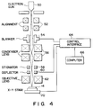
- This embodiment is a method of manufacturing dots of diffraction gratings by interference of two laser beams.
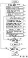
- step f2, g2, and h2 the pitch and direction of a diffraction grating and an exposure time are determined on the basis of these data and the light source position and the view direction input in step c2.
- the direction of the diffraction grating are obtained by using the above-mentioned equations.
- angle ⁇ of a 1st-order diffracted light is small, the pitch of the diffraction gratings depends on only a reproduced light color. Therefore the pitch corresponding to the color of the dot is selected from the pitches of the R, G and B.
- U.S. Serial No. 276,469 on November 25, 1988 is incorporated as a reference.
Landscapes
- Physics & Mathematics (AREA)
- General Physics & Mathematics (AREA)
- Optics & Photonics (AREA)
- Diffracting Gratings Or Hologram Optical Elements (AREA)
- Optical Integrated Circuits (AREA)
- Holo Graphy (AREA)
- Investigating Materials By The Use Of Optical Means Adapted For Particular Applications (AREA)
- Testing, Inspecting, Measuring Of Stereoscopic Televisions And Televisions (AREA)
- Analysing Materials By The Use Of Radiation (AREA)
Claims (4)
- Verfahren zur Herstellung einer Anzeigevorrichtung (15) mit einer Vielzahl von Beugungspunkten (16); die zum Ermöglichen einer Beobachtung eines Objekts (85) mit Parallaxe angeordnet sind, mit den Schritten:(a) eines Aufzeichnens einer Vielzahl von zweidimensionalen Bildern (80) des Objekts (85) aus einer Vielzahl von Positionen, damit eine Vielzahl von Ansichten des Objekts (85) erhalten wird, und eines Eingebens dieser Bilder (80) in einen Computer (82),(b) eines Auswählens von Bilddaten entsprechend einem ersten der Vielzahl von Bildern (80),(c) eines Eingebens von Daten entsprechend der Position einer Wiedergabe-Lichtquelle (91) und der Blickrichtung der Anzeigevorrichtung (15) in den Computer (82),(d) eines Lesens von Bilddaten entsprechend einem vorbestimmten Punkt (16) des ersten Bildes,(e) eines Bestimmens für den Punkt auf der Grundlage der Daten der Position der Wiedergabe-Lichtquelle, der Blickrichtung und der Punktdaten, der Punktfläche, des Abstands (d) sowie der Richtung (Ω) eines Beugungsgitters (18) derart, daß Licht von der Quelle (91) in der Blickrichtung gebeugt wird,(f) eines Bewegens eines X-Y-Stands (20), auf dem eine strahlungsempfindliche Platte (14) in einer Position angeordnet ist, die der des Punktes (16) entspricht, und eines Aufzeichnens des Gitters (18) in der Platte (14) durch Verwendung einer Elektronen-Abtasteinheit (50 bis 62),(g) eines sequentiellen Verarbeitens sämtlicher Daten, die dem ersten Bild entsprechen, durch Wiederholen der Schritte (d) bis (f) für jeden Punkt (16) des ersten Bildes und(h) eines Auswählens von Bilddaten, die einem anderen der Bilder (80) entsprechen, und eines Wiederholens der Schritte (c) bis (g), bis die Bilddaten sämtlicher Bilder (80) verarbeitet sind.
- Verfahren nach Anspruch 1, wobei eine Richtung Ω und ein Abstand d des Beugungsgitters (18) gemäß den folgenden Gleichungen erhalten werden:


- Verfahren zur Herstellung einer Anzeigevorrichtung (15) mit einer Vielzahl von Beugungspunkten (116), die zum Ermöglichen einer Beobachtung eines Objekts (85) mit Parallaxe durch Verwendung eines Zweistrahl-Interferenzverfahrens angeordnet sind, mit den Schritten:(a) eines Aufzeichnens einer Vielzahl von zweidimensionalen Bildern (80) des Objekts (85) aus einer Vielzahl von Positionen, damit eine Vielzahl von Ansichten des Objekts (85) erhalten wird, und eines Eingebens dieser Bilder (80) in einen Computer (82),(b) eines Auswählens von Bilddaten entsprechend einem ersten der Vielzahl von Bildern (80),(c) eines Eingebens von Daten entsprechend einer Position einer Wiedergabe-Lichtquelle (91) und der Blickrichtung der Anzeigevorrichtung (15) in den Computer (82),(d) eines Lesens von Bilddaten entsprechend einem vorbestimmten Punkt (116) des ersten Bildes,(e) eines Bestimmens für den Punkt (116) auf der Grundlage der Daten der Position der Wiedergabe-Lichtquelle, der Blickrichtung und der Punktdaten, der Belichtungszeit, des Abstands (d) sowie der Richtung (Ω) eines Beugungsgitters (118) derart, daß Licht von der Quelle (91) in der Blickrichtung gebeugt wird,(f) eines Bewegens eines X-Y-Θ-Stands (120, 128), auf dem eine strahlungsempfindliche Platte (114) in einer Position angeordnet ist, die der des Punktes (116) entspricht, und eines Bildens des Gitters (118) in der Platte (114) durch Verwendung eines Zweistrahl-Interferenzverfahrens,(g) eines sequentiellen Verarbeitens sämtlicher Daten, die dem ersten Bild entsprechen, durch Wiederholen der Schritte (d) bis (f) für jeden Punkt (116) des ersten Bildes und(h) eines Auswählens von Bilddaten, die einem anderen der Bilder (80) entsprechen, und eines Wiederholens der Schritte (c) bis (g), bis die Bilddaten sämtlicher Bilder (80) verarbeitet sind.
- Verfahren nach Anspruch 3, wobei eine Richtung Ω des Beugungsgitters (118) gemäß der folgenden Gleichung erhalten wird:

Applications Claiming Priority (2)
| Application Number | Priority Date | Filing Date | Title |
|---|---|---|---|
| JP268780/89 | 1989-10-16 | ||
| JP26878089 | 1989-10-16 |
Publications (3)
| Publication Number | Publication Date |
|---|---|
| EP0423680A2 EP0423680A2 (de) | 1991-04-24 |
| EP0423680A3 EP0423680A3 (en) | 1992-03-18 |
| EP0423680B1 true EP0423680B1 (de) | 1995-09-13 |
Family
ID=17463185
Family Applications (1)
| Application Number | Title | Priority Date | Filing Date |
|---|---|---|---|
| EP90119739A Expired - Lifetime EP0423680B1 (de) | 1989-10-16 | 1990-10-15 | Verfahren zur Herstellung einer Anzeigevorrichtung mit Beugungsgitterstrukturen |
Country Status (7)
| Country | Link |
|---|---|
| US (1) | US5132812A (de) |
| EP (1) | EP0423680B1 (de) |
| JP (1) | JP2508387B2 (de) |
| AT (1) | ATE127936T1 (de) |
| AU (1) | AU616361B2 (de) |
| CA (1) | CA2027462C (de) |
| DE (1) | DE69022349T2 (de) |
Families Citing this family (79)
| Publication number | Priority date | Publication date | Assignee | Title |
|---|---|---|---|---|
| CA2060057C (en) * | 1991-01-29 | 1997-12-16 | Susumu Takahashi | Display having diffraction grating pattern |
| EP0534616B1 (de) * | 1991-08-29 | 1997-10-29 | Fujitsu Limited | Vorrichtung zum Aufzeichnen von Hologrammen und holographisches optisches Element |
| JP2725913B2 (ja) * | 1991-08-29 | 1998-03-11 | 富士通株式会社 | ホログラム描画装置 |
| JP2774398B2 (ja) * | 1991-09-17 | 1998-07-09 | 富士通株式会社 | ホログラム作成装置 |
| JPH0572407A (ja) * | 1991-09-11 | 1993-03-26 | Toppan Printing Co Ltd | 回折格子プロツター |
| JPH0572405A (ja) * | 1991-09-11 | 1993-03-26 | Toppan Printing Co Ltd | 回折格子プロツター |
| JP2830530B2 (ja) * | 1991-09-11 | 1998-12-02 | 凸版印刷株式会社 | 回折格子プロッター |
| US6219015B1 (en) | 1992-04-28 | 2001-04-17 | The Board Of Directors Of The Leland Stanford, Junior University | Method and apparatus for using an array of grating light valves to produce multicolor optical images |
| JPH0635391A (ja) * | 1992-07-20 | 1994-02-10 | Fujitsu Ltd | 立体表示装置 |
| JPH0635392A (ja) * | 1992-07-20 | 1994-02-10 | Fujitsu Ltd | 立体表示装置 |
| US5991078A (en) * | 1992-08-19 | 1999-11-23 | Dai Nippon Printing Co., Ltd. | Display medium employing diffraction grating and method of producing diffraction grating assembly |
| CA2183979A1 (en) * | 1994-02-28 | 1995-08-31 | Peter Leigh-Jones | Difraction surfaces and methods for the manufacture thereof |
| US5841579A (en) | 1995-06-07 | 1998-11-24 | Silicon Light Machines | Flat diffraction grating light valve |
| US5629801A (en) * | 1995-06-07 | 1997-05-13 | Silicon Light Machines | Diffraction grating light doubling collection system |
| US5798743A (en) * | 1995-06-07 | 1998-08-25 | Silicon Light Machines | Clear-behind matrix addressing for display systems |
| US5661592A (en) * | 1995-06-07 | 1997-08-26 | Silicon Light Machines | Method of making and an apparatus for a flat diffraction grating light valve |
| DE19623352C2 (de) * | 1996-06-12 | 1999-11-11 | Kurz Leonhard Fa | Verfahren zur Herstellung von eine räumlich gemusterte Oberfläche aufweisenden Druck- oder Prägezylindern |
| US6064404A (en) * | 1996-11-05 | 2000-05-16 | Silicon Light Machines | Bandwidth and frame buffer size reduction in a digital pulse-width-modulated display system |
| AUPO384796A0 (en) * | 1996-11-26 | 1996-12-19 | Commonwealth Scientific And Industrial Research Organisation | Colour image diffractive device |
| US5982553A (en) | 1997-03-20 | 1999-11-09 | Silicon Light Machines | Display device incorporating one-dimensional grating light-valve array |
| US6088102A (en) | 1997-10-31 | 2000-07-11 | Silicon Light Machines | Display apparatus including grating light-valve array and interferometric optical system |
| US6271808B1 (en) | 1998-06-05 | 2001-08-07 | Silicon Light Machines | Stereo head mounted display using a single display device |
| US6130770A (en) | 1998-06-23 | 2000-10-10 | Silicon Light Machines | Electron gun activated grating light valve |
| US6101036A (en) | 1998-06-23 | 2000-08-08 | Silicon Light Machines | Embossed diffraction grating alone and in combination with changeable image display |
| US6215579B1 (en) | 1998-06-24 | 2001-04-10 | Silicon Light Machines | Method and apparatus for modulating an incident light beam for forming a two-dimensional image |
| US6303986B1 (en) | 1998-07-29 | 2001-10-16 | Silicon Light Machines | Method of and apparatus for sealing an hermetic lid to a semiconductor die |
| US6872984B1 (en) | 1998-07-29 | 2005-03-29 | Silicon Light Machines Corporation | Method of sealing a hermetic lid to a semiconductor die at an angle |
| US6956878B1 (en) | 2000-02-07 | 2005-10-18 | Silicon Light Machines Corporation | Method and apparatus for reducing laser speckle using polarization averaging |
| US7177081B2 (en) | 2001-03-08 | 2007-02-13 | Silicon Light Machines Corporation | High contrast grating light valve type device |
| US6865346B1 (en) | 2001-06-05 | 2005-03-08 | Silicon Light Machines Corporation | Fiber optic transceiver |
| US6747781B2 (en) | 2001-06-25 | 2004-06-08 | Silicon Light Machines, Inc. | Method, apparatus, and diffuser for reducing laser speckle |
| US6782205B2 (en) | 2001-06-25 | 2004-08-24 | Silicon Light Machines | Method and apparatus for dynamic equalization in wavelength division multiplexing |
| US6829092B2 (en) | 2001-08-15 | 2004-12-07 | Silicon Light Machines, Inc. | Blazed grating light valve |
| US6930364B2 (en) | 2001-09-13 | 2005-08-16 | Silicon Light Machines Corporation | Microelectronic mechanical system and methods |
| US6956995B1 (en) | 2001-11-09 | 2005-10-18 | Silicon Light Machines Corporation | Optical communication arrangement |
| US6800238B1 (en) | 2002-01-15 | 2004-10-05 | Silicon Light Machines, Inc. | Method for domain patterning in low coercive field ferroelectrics |
| US6767751B2 (en) | 2002-05-28 | 2004-07-27 | Silicon Light Machines, Inc. | Integrated driver process flow |
| US6728023B1 (en) | 2002-05-28 | 2004-04-27 | Silicon Light Machines | Optical device arrays with optimized image resolution |
| US7054515B1 (en) | 2002-05-30 | 2006-05-30 | Silicon Light Machines Corporation | Diffractive light modulator-based dynamic equalizer with integrated spectral monitor |
| US6822797B1 (en) | 2002-05-31 | 2004-11-23 | Silicon Light Machines, Inc. | Light modulator structure for producing high-contrast operation using zero-order light |
| US6829258B1 (en) | 2002-06-26 | 2004-12-07 | Silicon Light Machines, Inc. | Rapidly tunable external cavity laser |
| US6813059B2 (en) | 2002-06-28 | 2004-11-02 | Silicon Light Machines, Inc. | Reduced formation of asperities in contact micro-structures |
| US6908201B2 (en) | 2002-06-28 | 2005-06-21 | Silicon Light Machines Corporation | Micro-support structures |
| US7057795B2 (en) | 2002-08-20 | 2006-06-06 | Silicon Light Machines Corporation | Micro-structures with individually addressable ribbon pairs |
| US6801354B1 (en) | 2002-08-20 | 2004-10-05 | Silicon Light Machines, Inc. | 2-D diffraction grating for substantially eliminating polarization dependent losses |
| US6712480B1 (en) | 2002-09-27 | 2004-03-30 | Silicon Light Machines | Controlled curvature of stressed micro-structures |
| US6928207B1 (en) | 2002-12-12 | 2005-08-09 | Silicon Light Machines Corporation | Apparatus for selectively blocking WDM channels |
| US7057819B1 (en) | 2002-12-17 | 2006-06-06 | Silicon Light Machines Corporation | High contrast tilting ribbon blazed grating |
| US6987600B1 (en) | 2002-12-17 | 2006-01-17 | Silicon Light Machines Corporation | Arbitrary phase profile for better equalization in dynamic gain equalizer |
| US6934070B1 (en) | 2002-12-18 | 2005-08-23 | Silicon Light Machines Corporation | Chirped optical MEM device |
| US6927891B1 (en) | 2002-12-23 | 2005-08-09 | Silicon Light Machines Corporation | Tilt-able grating plane for improved crosstalk in 1×N blaze switches |
| US7068372B1 (en) | 2003-01-28 | 2006-06-27 | Silicon Light Machines Corporation | MEMS interferometer-based reconfigurable optical add-and-drop multiplexor |
| US7286764B1 (en) | 2003-02-03 | 2007-10-23 | Silicon Light Machines Corporation | Reconfigurable modulator-based optical add-and-drop multiplexer |
| US6947613B1 (en) | 2003-02-11 | 2005-09-20 | Silicon Light Machines Corporation | Wavelength selective switch and equalizer |
| US6922272B1 (en) | 2003-02-14 | 2005-07-26 | Silicon Light Machines Corporation | Method and apparatus for leveling thermal stress variations in multi-layer MEMS devices |
| US6806997B1 (en) | 2003-02-28 | 2004-10-19 | Silicon Light Machines, Inc. | Patterned diffractive light modulator ribbon for PDL reduction |
| US6829077B1 (en) | 2003-02-28 | 2004-12-07 | Silicon Light Machines, Inc. | Diffractive light modulator with dynamically rotatable diffraction plane |
| US7027202B1 (en) | 2003-02-28 | 2006-04-11 | Silicon Light Machines Corp | Silicon substrate as a light modulator sacrificial layer |
| US6922273B1 (en) | 2003-02-28 | 2005-07-26 | Silicon Light Machines Corporation | PDL mitigation structure for diffractive MEMS and gratings |
| US7391973B1 (en) | 2003-02-28 | 2008-06-24 | Silicon Light Machines Corporation | Two-stage gain equalizer |
| US7042611B1 (en) | 2003-03-03 | 2006-05-09 | Silicon Light Machines Corporation | Pre-deflected bias ribbons |
| EP1676157B9 (de) * | 2003-10-15 | 2011-09-07 | Giesecke & Devrient GmbH | Verfahren zum Erzeugen eines ebenen oder gekrümmten Gitterbildes |
| DE102005017355A1 (de) * | 2005-04-14 | 2006-10-19 | Giesecke & Devrient Gmbh | Beugungsgitter und Verfahren zu seiner Herstellung |
| JP4779415B2 (ja) * | 2005-04-18 | 2011-09-28 | 大日本印刷株式会社 | 画像形成方法及び画像表示体 |
| DE102005032997A1 (de) | 2005-07-14 | 2007-01-18 | Giesecke & Devrient Gmbh | Gitterbild und Verfahren zu seiner Herstellung |
| WO2007089770A2 (en) * | 2006-01-31 | 2007-08-09 | Polychromix Corporation | Hand-held ir spectrometer with a fixed grating and a diffractive mems-array |
| JP5488581B2 (ja) * | 2006-08-22 | 2014-05-14 | 大日本印刷株式会社 | 立体模様が表現された回折格子記録媒体の作成方法 |
| US7891818B2 (en) | 2006-12-12 | 2011-02-22 | Evans & Sutherland Computer Corporation | System and method for aligning RGB light in a single modulator projector |
| US8358317B2 (en) | 2008-05-23 | 2013-01-22 | Evans & Sutherland Computer Corporation | System and method for displaying a planar image on a curved surface |
| US8702248B1 (en) | 2008-06-11 | 2014-04-22 | Evans & Sutherland Computer Corporation | Projection method for reducing interpixel gaps on a viewing surface |
| KR101539935B1 (ko) * | 2008-06-24 | 2015-07-28 | 삼성전자주식회사 | 3차원 비디오 영상 처리 방법 및 장치 |
| US20090317062A1 (en) * | 2008-06-24 | 2009-12-24 | Samsung Electronics Co., Ltd. | Image processing method and apparatus |
| KR101560617B1 (ko) * | 2008-09-10 | 2015-10-16 | 삼성전자주식회사 | 광 발생 장치 및 그 제어 방법 |
| US8077378B1 (en) | 2008-11-12 | 2011-12-13 | Evans & Sutherland Computer Corporation | Calibration system and method for light modulation device |
| JP5419540B2 (ja) * | 2009-05-18 | 2014-02-19 | パナソニック株式会社 | 構造発色体 |
| US9641826B1 (en) | 2011-10-06 | 2017-05-02 | Evans & Sutherland Computer Corporation | System and method for displaying distant 3-D stereo on a dome surface |
| CN103246195B (zh) * | 2013-05-08 | 2015-12-02 | 苏州苏大维格光电科技股份有限公司 | 三维激光打印方法与系统 |
| US10054859B2 (en) | 2016-01-06 | 2018-08-21 | Soochow University | Real-time variable parameter micro-nano optical field modulation system and interference lithography system |
| CN105511074B (zh) * | 2016-01-06 | 2018-01-09 | 苏州大学 | 实时变参量微纳米光场调制系统和干涉光刻系统 |
Family Cites Families (10)
| Publication number | Priority date | Publication date | Assignee | Title |
|---|---|---|---|---|
| US3646335A (en) * | 1969-02-11 | 1972-02-29 | Us Army | Recorder correlator using scanning recorder devices |
| US3832027A (en) * | 1969-03-12 | 1974-08-27 | Bell Telephone Labor Inc | Synthetic hologram generation from a plurality of two-dimensional views |
| US4498740A (en) * | 1983-04-18 | 1985-02-12 | Aerodyne, Research, Inc. | Hologram writer and method |
| EP0213726B1 (de) * | 1985-07-26 | 1993-03-03 | Matsushita Electric Industrial Co., Ltd. | Holographische Multiplex/Demultiplexvorrichtung, und ihr Herstellungsverfahren |
| US4846552A (en) * | 1986-04-16 | 1989-07-11 | The United States Of America As Represented By The Secretary Of The Air Force | Method of fabricating high efficiency binary planar optical elements |
| US4778262A (en) * | 1986-10-14 | 1988-10-18 | American Bank Note Holographics, Inc. | Computer aided holography and holographic computer graphics |
| EP0311340B1 (de) * | 1987-10-05 | 1993-08-04 | Matsushita Electric Industrial Co., Ltd. | Optische Lesekopf |
| US5058992A (en) * | 1988-09-07 | 1991-10-22 | Toppan Printing Co., Ltd. | Method for producing a display with a diffraction grating pattern and a display produced by the method |
| US4896044A (en) * | 1989-02-17 | 1990-01-23 | Purdue Research Foundation | Scanning tunneling microscope nanoetching method |
| US5016953A (en) * | 1989-08-31 | 1991-05-21 | Hughes Aircraft Company | Reduction of noise in computer generated holograms |
-
1990
- 1990-09-05 JP JP2233105A patent/JP2508387B2/ja not_active Expired - Lifetime
- 1990-10-12 CA CA002027462A patent/CA2027462C/en not_active Expired - Lifetime
- 1990-10-12 AU AU64597/90A patent/AU616361B2/en not_active Expired
- 1990-10-15 DE DE69022349T patent/DE69022349T2/de not_active Expired - Lifetime
- 1990-10-15 US US07/597,229 patent/US5132812A/en not_active Expired - Lifetime
- 1990-10-15 AT AT90119739T patent/ATE127936T1/de not_active IP Right Cessation
- 1990-10-15 EP EP90119739A patent/EP0423680B1/de not_active Expired - Lifetime
Also Published As
| Publication number | Publication date |
|---|---|
| AU6459790A (en) | 1991-05-23 |
| CA2027462C (en) | 1998-08-11 |
| EP0423680A3 (en) | 1992-03-18 |
| DE69022349D1 (de) | 1995-10-19 |
| CA2027462A1 (en) | 1991-04-17 |
| AU616361B2 (en) | 1991-10-24 |
| EP0423680A2 (de) | 1991-04-24 |
| JP2508387B2 (ja) | 1996-06-19 |
| JPH03206401A (ja) | 1991-09-09 |
| US5132812A (en) | 1992-07-21 |
| DE69022349T2 (de) | 1996-02-08 |
| ATE127936T1 (de) | 1995-09-15 |
Similar Documents
| Publication | Publication Date | Title |
|---|---|---|
| EP0423680B1 (de) | Verfahren zur Herstellung einer Anzeigevorrichtung mit Beugungsgitterstrukturen | |
| US5058992A (en) | Method for producing a display with a diffraction grating pattern and a display produced by the method | |
| US5301062A (en) | Display having diffraction grating pattern | |
| JP2979951B2 (ja) | 回折格子パターンを有するディスプレイ | |
| US20020171883A1 (en) | System for making a hologram of an image | |
| JPS62232616A (ja) | 連続調カラ−画像のフルカラ−再生方法および装置 | |
| JP3283582B2 (ja) | 回折格子アレイおよびそれを用いた立体像表示装置 | |
| JPH0272320A (ja) | 回折格子パターンを有するディスプレイの作製方法 | |
| JP2745902B2 (ja) | 回折格子パターンを有するディスプレイ | |
| JPH03180801A (ja) | 回析格子パターンを良するディスプレイの作製方法 | |
| JP2976774B2 (ja) | 回折格子パターンを有するディスプレイ | |
| JP2586230B2 (ja) | 回折格子パターンを有するディスプレイ | |
| JP2630047B2 (ja) | 回折格子パターンを有するディスプレイおよびその作製方法 | |
| KR101962213B1 (ko) | 표면 요철형 미세픽셀의 회절을 이용하여 입체영상이 나타나는 글래스 마스터 제작방법 | |
| JPH0820563B2 (ja) | 回折格子パターンを有するディスプレイ | |
| JP3248371B2 (ja) | 立体像表示装置 | |
| JP4325017B2 (ja) | 回折格子パターンの作製方法 | |
| JP2822798B2 (ja) | ホログラムの作製方法 | |
| JP3932599B2 (ja) | 回折格子パターン | |
| JPH0272319A (ja) | 回折格子パターンを有するディスプレイの作製方法 | |
| JP2803377B2 (ja) | レインボー・ホログラムの作成方法 | |
| JP3438249B2 (ja) | 大型フルカラーホログラフィックステレオグラムの作製方法および装置 | |
| JP2830530B2 (ja) | 回折格子プロッター | |
| JP3951576B2 (ja) | 回折格子パターン | |
| JP3590982B2 (ja) | マイクロ・ミラー・デバイスを用いた立体・可変画像表示装置 |
Legal Events
| Date | Code | Title | Description |
|---|---|---|---|
| PUAI | Public reference made under article 153(3) epc to a published international application that has entered the european phase |
Free format text: ORIGINAL CODE: 0009012 |
|
| 17P | Request for examination filed |
Effective date: 19901015 |
|
| AK | Designated contracting states |
Kind code of ref document: A2 Designated state(s): AT CH DE FR GB LI |
|
| PUAL | Search report despatched |
Free format text: ORIGINAL CODE: 0009013 |
|
| AK | Designated contracting states |
Kind code of ref document: A3 Designated state(s): AT CH DE FR GB LI |
|
| 17Q | First examination report despatched |
Effective date: 19940202 |
|
| GRAA | (expected) grant |
Free format text: ORIGINAL CODE: 0009210 |
|
| AK | Designated contracting states |
Kind code of ref document: B1 Designated state(s): AT CH DE FR GB LI |
|
| REF | Corresponds to: |
Ref document number: 127936 Country of ref document: AT Date of ref document: 19950915 Kind code of ref document: T |
|
| ET | Fr: translation filed | ||
| REF | Corresponds to: |
Ref document number: 69022349 Country of ref document: DE Date of ref document: 19951019 |
|
| PLBE | No opposition filed within time limit |
Free format text: ORIGINAL CODE: 0009261 |
|
| STAA | Information on the status of an ep patent application or granted ep patent |
Free format text: STATUS: NO OPPOSITION FILED WITHIN TIME LIMIT |
|
| 26N | No opposition filed | ||
| REG | Reference to a national code |
Ref country code: GB Ref legal event code: IF02 |
|
| REG | Reference to a national code |
Ref country code: CH Ref legal event code: PFA Owner name: TOPPAN PRINTING CO., LTD Free format text: TOPPAN PRINTING CO., LTD#5-1, TAITO 1-CHOME#TAITO-KU/TOKYO (JP) -TRANSFER TO- TOPPAN PRINTING CO., LTD#5-1, TAITO 1-CHOME#TAITO-KU/TOKYO (JP) |
|
| PGFP | Annual fee paid to national office [announced via postgrant information from national office to epo] |
Ref country code: AT Payment date: 20091013 Year of fee payment: 20 Ref country code: CH Payment date: 20091014 Year of fee payment: 20 Ref country code: DE Payment date: 20091008 Year of fee payment: 20 |
|
| PGFP | Annual fee paid to national office [announced via postgrant information from national office to epo] |
Ref country code: GB Payment date: 20091014 Year of fee payment: 20 Ref country code: FR Payment date: 20091029 Year of fee payment: 20 |
|
| REG | Reference to a national code |
Ref country code: CH Ref legal event code: PL |
|
| REG | Reference to a national code |
Ref country code: GB Ref legal event code: PE20 Expiry date: 20101014 |
|
| PG25 | Lapsed in a contracting state [announced via postgrant information from national office to epo] |
Ref country code: GB Free format text: LAPSE BECAUSE OF EXPIRATION OF PROTECTION Effective date: 20101014 |
|
| PG25 | Lapsed in a contracting state [announced via postgrant information from national office to epo] |
Ref country code: DE Free format text: LAPSE BECAUSE OF EXPIRATION OF PROTECTION Effective date: 20101015 |