EP0423970B1 - Elektrischer Verbinder mit geringer Einschubkraft und geringer Leiterplattenbelastung - Google Patents
Elektrischer Verbinder mit geringer Einschubkraft und geringer Leiterplattenbelastung Download PDFInfo
- Publication number
- EP0423970B1 EP0423970B1 EP90310783A EP90310783A EP0423970B1 EP 0423970 B1 EP0423970 B1 EP 0423970B1 EP 90310783 A EP90310783 A EP 90310783A EP 90310783 A EP90310783 A EP 90310783A EP 0423970 B1 EP0423970 B1 EP 0423970B1
- Authority
- EP
- European Patent Office
- Prior art keywords
- contact
- board
- cavity
- housing
- latch
- Prior art date
- Legal status (The legal status is an assumption and is not a legal conclusion. Google has not performed a legal analysis and makes no representation as to the accuracy of the status listed.)
- Expired - Lifetime
Links
- 238000003780 insertion Methods 0.000 title claims description 7
- 230000037431 insertion Effects 0.000 title claims description 7
- 235000012431 wafers Nutrition 0.000 claims description 29
- 230000001154 acute effect Effects 0.000 claims description 4
- 230000013011 mating Effects 0.000 claims description 4
- 239000000463 material Substances 0.000 claims description 2
- 230000035515 penetration Effects 0.000 claims description 2
- 230000000149 penetrating effect Effects 0.000 claims 3
- 230000001681 protective effect Effects 0.000 claims 1
- 238000000034 method Methods 0.000 description 3
- 238000000465 moulding Methods 0.000 description 2
- 230000004323 axial length Effects 0.000 description 1
- 230000001186 cumulative effect Effects 0.000 description 1
- 229920001169 thermoplastic Polymers 0.000 description 1
- 239000004416 thermosoftening plastic Substances 0.000 description 1
Images


Classifications
-
- H—ELECTRICITY
- H01—ELECTRIC ELEMENTS
- H01R—ELECTRICALLY-CONDUCTIVE CONNECTIONS; STRUCTURAL ASSOCIATIONS OF A PLURALITY OF MUTUALLY-INSULATED ELECTRICAL CONNECTING ELEMENTS; COUPLING DEVICES; CURRENT COLLECTORS
- H01R12/00—Structural associations of a plurality of mutually-insulated electrical connecting elements, specially adapted for printed circuits, e.g. printed circuit boards [PCB], flat or ribbon cables, or like generally planar structures, e.g. terminal strips, terminal blocks; Coupling devices specially adapted for printed circuits, flat or ribbon cables, or like generally planar structures; Terminals specially adapted for contact with, or insertion into, printed circuits, flat or ribbon cables, or like generally planar structures
- H01R12/70—Coupling devices
- H01R12/82—Coupling devices connected with low or zero insertion force
- H01R12/83—Coupling devices connected with low or zero insertion force connected with pivoting of printed circuits or like after insertion
Definitions
- This invention relates to electrical connectors for making electrical connections to printed circuit boards. More particularly, this invention relates to zero or low insertion force electrical connectors for making electrical connections to conductive strips mounted along the edges of printed circuit boards.
- Zero insertion force connectors are disclosed in US-A-4,575,172 and US-A-3,848,952. These connectors generally consist of a housing enclosing a pair of generally C-shaped or U-shaped electrical contact arms of differing lengths. The edge of the printed circuit board is inserted between the arms without making contact with either arm. The board is then rotated into position in the housing so that one arm engages one side of the edge of the board and the second arm engages the opposing side of the edge of the board. At least one arm thus engages a contact on the edge of the board with sufficient normal force to assure electrical contact, but without any wiping between the arm and the contact.
- the contacts are exposed to direct impact against the edge of a printed circuit board when the board is inserted out of alignment into the connector or when the board edge is warped to a significant degree. This direct impact can damage the contacts in the connector as well as the contacts on the edge of the board.
- US-A-3,732,531 discloses an electrical connector according to the preamble of claim 1.
- the present invention is characterised by the features of the characterising portion of claim 1.
- the present invention is a low-insertion-force electrical connector for connecting a daughter circuit board to a mother circuit board, the daughter circuit board having an edge, first and second opposed surfaces abutting the edge, and at least one contact on one of the two opposed surfaces
- the electrical connector comprising a housing having a plurality of adjacent insulating wafers spaced apart and joined by two opposing ramp means, each wafer having a wafer cavity, whereby adjacent wafers cooperatively provide a board cavity for penetration of the daughter board edge into the board cavity in the housing, and at least one contact disposed in the space between a pair of adjacent wafers, the contact having a pair of opposing contact spring means disposed in the board cavity between adjacent wafers, and a pair of latch arms, each latch arm having an inclined latch surface for mating contact with the ramp means, the inclined surfaces and ramp means cooperatively providing means for positioning the contact in the housing.
- FIG 1 of the drawing shows the housing, generally 10, for an electrical connector housing having shrouded contacts such as shown in Figure 2.
- the housing 10 is made of a suitable insulating thermoplastic.
- the housing 10 consists of a series of interconnected, insulating, parallel, uniformly spaced wafers, 12, 14, 13. Adjacent wafers 12, 14 are interconnected by: (i) a central stop web 16, (ii) a first outer ramp 18 spaced from one side of the stop web 16, (iii) a second outer ramp 20 spaced from the other side of the stop web 16, (iv) a first shroud 22 between the first ramp 18 and the stop web 16, and (v) a second shroud 24 between the second ramp 20 and stop web 16.
- the stop web 16, first and second ramps 18, 20, and first and second shrouds 22, 24 extend the entire axial length A of the housing 10, providing substantial torsional stability and rigidity to the connector housing 10 with a minimum of housing material.
- Each wafer, 13 for example has a planar body 26 with a planar bottom edge 27 of the perpendicular to the plane of the wafer's body 26.
- a cavity 28 penetrates the central section of the body 26 on the side of the body 26 opposite the bottom edge 27 of the body 26.
- the cavity 28 is bounded by a first wall section 30, a second wall section 32 opposing the first wall section 30, and a flatted base section 34 interconnecting the two wall sections 30, 32.
- the first wall 30 has a first planar cavity side 35 adjacent the cavity 28 and extending perpendicularly from the planar cavity bottom 37 of the flatted base section 34.
- the first shroud 22 extends perpendicularly from the first wall 30 toward, and to interconnect with, the adjacent wafer 36.
- the first shroud 22 also extends perpendicularly from the plane of the cavity side of the first wall 30 to penetrate the cavity 28.
- the second wall 32 has a second planar cavity side 40 that also extends perpendicularly from the planar cavity bottom 37 of the flatted base section 34.
- the second wall 32 also has a third planar cavity side 42 that extends from the second cavity side 40 away from the cavity bottom 37.
- the second shroud 24 extends perpendicularly from the second wall 32 toward, and to interconnect with, the adjacent wafer 36.
- the second shroud 24 has an inclined cavity side 44 co-planar with, and partially coextensive with, the plane of the third cavity side 42 on the second wall 32.
- the inclined cavity side 44 and the third cavity side 42 thus cooperatively provide an inclined ramp into a deep throat area in the cavity 28 bounded by the first cavity side 35, bottom cavity side or throat 37, and second cavity side 40.
- the first ramp 18 has a first inner inclined surface 46 and a second inner inclined surface 48.
- the first and second inner inclined surfaces 46, 48 are parallel, but spaced apart and interconnected by a planar inner wall 47 parallel to but spaced from the first planar side 35 of the first wall section 30.
- the angle of incline for the inclined surface 46 is acute to the plane of the cavity's flatted base section 34, and the incline is toward the flatted base section 34 from the edges of the inclined surfaces 46, 48 furthest from the flatted base section 34.
- the second inclined surface 48 is at the distal end 50 of the first ramp 18 furthest from the base section 34.
- the upper end 52 of the first ramp 18 is flatted and perpendicular to the planes of the wafers 12, 14, 13, 36. As measured from a line perpendicularly intersecting the upper end 52 and the plane of the distal end 50, the end 50 is spaced from the line on the side of the line opposite the flatted base section 34.
- the second ramp 20 is the mirror image of the first ramp 18 on the opposite side of the flatted base section 34. Where the first and second ramps 18, 20 are coextensive with the wafers, e.g., 14, third and fourth inclined shroud sections, 54, 56 respectively, extend perpendicularly from the back end, e.g., 52, of each such ramp, e.g., 18.
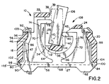
- the preferred embodiment of the shrouded type of contact 58 is mounted in the housing 10.
- the contact 58 and housing 10 cooperatively provide means for retaining the contact 58 in the housing 10 without placing any axial bowing stress on the housing 10 while simultaneously urging the lower contact pads 60, 62 on the contact 58 in a direction outwardly of and away from the bottom edge 27 of the housing 10 into contact with mating pads on a mother printed circuit board.
- the contact 58 has a G-shaped board contact section 64.
- the mid-section 66 of the G-shaped section 64 joins a transverse support member 68.
- the G-shaped member has a first contact arm 70 opposite a second contact arm 72 that extends from opposing sides of the mid-section 66 distal from the transverse support member 68.
- the first contact arm 70 is substantially longer than the second contact arm 72.
- the free ends 74, 76 of the opposing contact arms, 70, 72 respectively, extend from the mid-section 66 substantially perpendicularly from the support member 68.
- Each such free end 74, 76 also has a contact extension point, 78, 80 respectively, extending perpendicularly from their respective free ends 74, 76 toward each other 78, 80 in a plane parallel to the plane of the support member 68.
- the contact pads 60, 62 extend somewhat from the side of the support member 68 opposite the G-shaped contact 64.
- the pads 60, 62 are also spaced apart, extending from the opposing ends, 82, 84 respectively, of the support member 68.
- a first latch arm 86 and second latch arm 88 extend perpendicularly from the sides of the support member 68 opposite the contact pads 60, 62.
- the first latch arm 86 extends opposite the first contact pad 60
- the second latch arm extends opposite the second contact pad 62.
- the G-shaped contact section 64 is centered between, and spaced inwardly from, the substantially parallel first and second latch arms 86, 88.
- the latch arms 86, 88 are mirror images of each other.
- the first latch arm 86 for example, has an extension end 90 extending perpendicularly from the support member 68, a latch end 92 opposite the extension end 90, and an inclined mid-ramp 94 between its two ends 90, 92.
- the latch end 92 extends substantially perpendicularly from the latch arm 86 away from the G-shaped contact section 64.
- the latch end 92 also has an undercut 96 on the outermost edge of the latch end 92 nearest the support member 68.
- the inclined mid-ramp 94 is at an acute angle to the plane of the support member 68 in the direction of the G-shaped contact section 64. That angle, however, is slightly greater than that for the first inclined surface 46 of the first ramp 18 on the housing 10.
- the first latch arm 86 and second latch arm 88 are spaced somewhat laterally inwardly from the outermost opposing ends 98, 100 of the support member 68.
- the support member 86 thus has planar latch surfaces 102, 104 that extend perpendicularly from the latch arms, 86, 88 respectively, at the outermost ends, 98, 100 respectively, of the support member 86.
- the contact 64 is mounted in the housing 10 by forcing the housing 10 downwardly on the contact 64 in the orientation shown in Figure 2.
- the ramps 18, 20 on the housing 10 resiliently deflect the latch arms, 86, 88 respectively, inwardly toward the G-shaped contact section 64, until the second inclined surface 48 abuts the planar latch surface 102 of the support member 68.
- the latch end 92 is free to resiliently retract back toward its undeflected, free-state orientation as shown in Figure 2, because the distance between the undercut 96 and the latch surface 102 is slightly greater than the distance between the opposing mating ends 103, 105 of the first ramp 18.
- the first and second ramps 18, 20, are spaced apart, however, so that the first inclined surface 46 engages the mid-ramp 94 in the first latch arm 86 to urge it to deflect toward the G-shaped contact section 64.
- the opposite engagement of opposing surfaces at the second latch arm 86 and second ramp 20 combine to cooperatively urge the contact pads 60, 62 uniformly away form the cavity 28, and to simultaneously center the G-shaped contact 64 in the housing 10.
- the opposing contact sections 78, 80 penetrate the cavity 28.
- the first contact point 78 extends at a distance from the over stress lip 38 on the first shroud 22 toward the support member 68, and into the cavity 28 somewhat beyond the innermost cavity-penetrating edge 39 of the over-stress lip 38.
- the second contact point 80 reciprocally extends into the cavity 28 somewhat beyond the second cavity side 40 of the second wall section 32 in the vicinity of the junction of the second and third wall cavity sides 40, 42.
- a "daughter" printed circuit board 106 is mounted in the connector, generally 108, by inserting an edge 110 of the daughter board 106 into the cavity 28 at an acute angle to flatted base section 34 without appreciable contact between the daughter board 106 and the contact arms 70, 72.
- the daughter board 106 is then rotated into position perpendicular to the plane of the flatted base section 34.
- the contact extensions 78, 80 firmly engage respective sides 112, 114 of the daughter board 106 perpendicular to the planes of the sides 112, 114.
- the shrouds 22, 24, 54, 56 protect the contact 58 when the daughter board 106 is inserted in the connector 108.
- the first shroud 22 also serves, via its over-stress lip 38, as a board rotation stop, to prevent the daughter board 106 from deflecting the contact extensions 78, 80 any further than necessary to attain optional pressure of the extensions 78, 80 against the respective sides 112, 114 of the daughter board 106.
- the flatted base section 34 and stop 36 provide a strong, rigid board stop, preventing the daughter board 106 from ramming or contacting the mid-section 66 of the contact 88.
- the daughter board 106 may be maintained in the position shown in phantom in Figure 2, i.e. with the contact sections engaged with the daughter board as previously described, by a latch means 180 (see Figure 3) adjacent the ends of the daughter board slot in the housing 10.
Landscapes
- Coupling Device And Connection With Printed Circuit (AREA)
Claims (7)
- Elektrischer Verbinder mit geringer Einschubkraft zum Verbinden einer Tochterleiterplatte (106) mit einer Mutterleiterplatte, wobei die Tochterleiterplatte (106) einen Rand (110), eine erste und eine zweite Oberfläche in Gegenüberlage, die an den Rand anstoßen, und zumindest einen Kontakt an einer der beiden gegenüberliegenden Oberflächen aufweist und wobei der elektrische Verbinder versehen ist mita. einem Gehäuse (10) mit einer Mehrzahl aneinandergrenzender isolierender Plättchen (12,14) im Abstand zueinander und verbunden durch zwei einander gegenüberliegende Rampeneinrichtungen (18,20), wobei jedes Plättchen einen Plättchenhohlraum (28) besitzt, wodurch benachbarte Plättchen (12,14) zusammenwirkend einen Plattenhohlraum für das Eindringen des Tochterplattenrandes (110) in den Plattenhohlraum im Gehäuse (10) bilden, undb. zumindest einem Kontakt (58), der in dem Raum zwischen einem Paar benachbarter Plättchen (12,14) angeordnet ist, wobei der Kontakt (58) ein Paar einander gegenüberliegender Federkontakteinrichtungen (78,80) im Plattenhohlraum zwischen benachbarten Plättchen (12,14) und ein Paar von Verriegelungsarmen (86,88) besitzt, jeder Verriegelungsarm (86,88) eine schräge Verriegelungsfläche (94) für einen Gegenkontakt mit der Rampeneinrichtung (18,20) aufweist und die schrägen Flächen (94) und die Rampeneinrichtungen (18,20) zusammenwirkend eine Einrichtung zum Positionieren des Kontakts (58) im Gehäuse (10) bilden,dadurch gekennzeichnet, daß das Gehäuse (10) so gestaltet ist, daß es das Einschieben der Tochterplatte (106) mit einer ersten Winkelausrichtung mit geringer Einschubkraft und Drehung in eine zweite Betriebswinkelausrichtung ermöglicht, in der der Kontaktteil der Tochterplatte (106) mit zumindest einer der Federekontakteinrichtungen (78,80) in Wirkeingriff steht, und eine Einrichtung (180) zum Halten der Tochterplatte (106) in der zweiten Betriebswinkelausrichtung aufweist und
das Gehäuse zumindest eine erste Ummantelung (22) und eine zweite Ummantelung (24) besitzt, wobei die erste Ummantelung (22) einen wesentlichen Bereich eines in den Hohlraum (58) eindringenden Kontaktarms (88) abschirmt und einen Anschlag gegen Überbeanspruchung zum Verhindern einer Überdrehung der Tochterplatte (106) bildet, und die erste und zweite Ummantelung (22,24) jeweils benachbarte Plättchen (12,14) des Gehäuses (10) miteinander verbinden. - Verbinder nach Anspruch 1, bei dema. das Gehäuse (10) eine Tochterplattenmontageseite gegenüber einer Mutterplattenmontageseite aufweist, wobei die Mehrzahl der Plättchen (12,14) in die Tochterplattenmontageseite eindringt,b. jede Rampeneinrichtung (18,20) einen langgestreckten Abschnitt mit gegenüberliegenden Rampenenden (103,105) und zumindest einer schrägen Rampenfläche (46) zwischen den gegenüberliegenden Enden in einem spitzen Winkel zur Mutterplattenmontageseite des Gehäuses umfaßt undc. jeder Verriegelungsarm (86,88) einander gegenüberliegende Verriegelungsenden (92,102) aufweist, die voneinander weiter als der Abstand zwischen den gegenüberliegenden Rampenenden (103,105) beabstandet sind, die schräge Verriegelungsfläche (94) zwischen den gegenüberliegenden Verriegelungsenden (103,105) des Verriegelungsarms (86) liegt und die schrägen Verriegelungsflächen (46) an den gegenüberliegenden Verriegelungsarmen (86,88) mit im wesentlichen gleichen und entgegengesetzten Winkeln verlaufen.
- Verbinder nach einem beliebigen vorhergehenden Anspruch, bei dem die Plättchen ferner durch eine Anschlageinrichtung (38) angrenzend an eine Hohlraumverengung im Hohlraum (28) miteinander verbunden sind.
- Verbinder nach einem beliebigen vorhergehenden Anspruch, bei dem zumindest ein Plättchen (141) zumindest eine Ausnehmung (142,144) im Plättchen aufweist, um das Material im Plättchen (141) zu minimieren und die zur Herstellung des Verbinders verwendete Form ohne einen übermäßigen Verlust an Festigkeit für den Verbinder zu verstärken.
- Verbinder nach einem beliebigen vorhergehenden Anspruch, dadurch gekennzeichnet, daß zumindest ein Kontakt (i) ein die Federkontaktarme abstützendes Stützglied und (ii) zumindest ein Plattenkontaktteil an der Gliedseite gegenüber der Federkontakteinrichtung aufweist.
- Verbinder nach einem der Ansprüche 1 bis 5, dadurch gekennzeichnet, daß jeder Verriegelungsarm (86,88) ein freigelegtes Ende angrenzend an den Plattenhohlraum besitzt und jedes Plättchen ferner eine schützende Verriegelungsummantelung angrenzend an den Plattenhohlraum aufweist, wodurch die freigelegten Enden der Verriegelungsarme (86,88) vor einer Berührung mit der Tochterplatte (106) geschützt sind.
- Verbinder nach Anspruch 6, bei dem die zweite Ummantelung (24) einen wesentlichen Bereich des in den Hohlraum (58) eindringenden anderen Kontaktarms (80) abschirmt.
Applications Claiming Priority (2)
| Application Number | Priority Date | Filing Date | Title |
|---|---|---|---|
| US07/422,703 US4957448A (en) | 1989-10-17 | 1989-10-17 | Low insertion force, low board stress electrical connector |
| US422703 | 1989-10-17 |
Publications (3)
| Publication Number | Publication Date |
|---|---|
| EP0423970A2 EP0423970A2 (de) | 1991-04-24 |
| EP0423970A3 EP0423970A3 (en) | 1992-02-26 |
| EP0423970B1 true EP0423970B1 (de) | 1995-06-14 |
Family
ID=23675998
Family Applications (1)
| Application Number | Title | Priority Date | Filing Date |
|---|---|---|---|
| EP90310783A Expired - Lifetime EP0423970B1 (de) | 1989-10-17 | 1990-10-02 | Elektrischer Verbinder mit geringer Einschubkraft und geringer Leiterplattenbelastung |
Country Status (4)
| Country | Link |
|---|---|
| US (1) | US4957448A (de) |
| EP (1) | EP0423970B1 (de) |
| JP (1) | JPH0630266B2 (de) |
| DE (1) | DE69020090T2 (de) |
Families Citing this family (8)
| Publication number | Priority date | Publication date | Assignee | Title |
|---|---|---|---|---|
| US5085593A (en) * | 1991-01-14 | 1992-02-04 | Kenny Tuan | Elasticity-enhanced contact element of electrical connector |
| US5174780A (en) * | 1991-03-29 | 1992-12-29 | Yang Lee Su Lan | Slant socket for memory module |
| US5061200A (en) * | 1991-03-29 | 1991-10-29 | Yang Lee Su Lan | Stress-dispersed contact element of low insertion force electrical connector |
| JPH0590867U (ja) * | 1992-05-22 | 1993-12-10 | デュポン・ジャパン・リミテッド | 電気コネクタ |
| US5292265A (en) * | 1993-03-02 | 1994-03-08 | Molex Incorporated | Edge mounted circuit board electrical connector |
| US5626487A (en) * | 1995-02-03 | 1997-05-06 | Hon Hai Precision Ind. Co., Ltd. | Contact for slanted SIMM socket |
| US5580267A (en) * | 1995-09-19 | 1996-12-03 | Molex Incorporated | Electrical connector for a printed circuit board |
| US5725389A (en) * | 1995-11-09 | 1998-03-10 | Molex Incorporated | Edge card connector |
Family Cites Families (7)
| Publication number | Priority date | Publication date | Assignee | Title |
|---|---|---|---|---|
| FR1543470A (fr) * | 1967-09-14 | 1968-10-25 | Socapex | Connecteur pour cartes imprimées |
| DE2621984B2 (de) * | 1976-05-18 | 1978-03-30 | Preh Elektrofeinmechanische Werke Jakob Preh Nachf., 8740 Bad Neustadt | Kontaktfederleiste |
| US4575172A (en) * | 1984-04-06 | 1986-03-11 | Molex Incorporated | Low insertion force electrical connector with stress controlled contacts |
| US4737120A (en) * | 1986-11-12 | 1988-04-12 | Amp Incorporated | Electrical connector with low insertion force and overstress protection |
| US4718859A (en) * | 1987-03-16 | 1988-01-12 | Molex Incorporated | Zero insertion force connector for flexible flat cable |
| US4832617A (en) * | 1988-03-31 | 1989-05-23 | Foxx Conn International, Inc. | Circuit board socket, contact and method of manufacture |
| US4826446A (en) * | 1988-05-04 | 1989-05-02 | Burndy Corporation | Electrical contact pins and assemblies |
-
1989
- 1989-10-17 US US07/422,703 patent/US4957448A/en not_active Expired - Fee Related
-
1990
- 1990-08-27 JP JP2225028A patent/JPH0630266B2/ja not_active Expired - Lifetime
- 1990-10-02 EP EP90310783A patent/EP0423970B1/de not_active Expired - Lifetime
- 1990-10-02 DE DE69020090T patent/DE69020090T2/de not_active Expired - Fee Related
Also Published As
| Publication number | Publication date |
|---|---|
| EP0423970A2 (de) | 1991-04-24 |
| JPH03145081A (ja) | 1991-06-20 |
| JPH0630266B2 (ja) | 1994-04-20 |
| EP0423970A3 (en) | 1992-02-26 |
| DE69020090T2 (de) | 1996-01-18 |
| DE69020090D1 (de) | 1995-07-20 |
| US4957448A (en) | 1990-09-18 |
Similar Documents
| Publication | Publication Date | Title |
|---|---|---|
| EP0569893B1 (de) | Elektrischer Flachbauverbinder | |
| EP0543278B1 (de) | Elektrischer Flachbauverbinder | |
| US5842875A (en) | Electric connector assembly for use in coupling two printed boards | |
| EP0356156B1 (de) | Randverbinder für Leiterplatten und Anschlusselement dafür | |
| US5478253A (en) | Electrostatic discharge contacts for blind mating connectors | |
| EP0664581A2 (de) | Niederprofilverbinder zwischen Leiterplatten | |
| EP0633631B1 (de) | Elektrischer Randverbinder für Leiterplatten | |
| EP0567007A2 (de) | Elektrischer Verbinder zur Oberflächenmontage | |
| JP3452662B2 (ja) | 基板用電気コネクタ及びその保持装置 | |
| EP0952632A2 (de) | Elektrischer Verbinder mit eingesetzten Anschlüssen | |
| US5080596A (en) | Connector with contact spacer plate providing greater lateral force on rear contacts | |
| EP0926779B1 (de) | Leiterplatten-Randverbinder hoher Kontaktdichte und dessen Herstellungsverfahren | |
| KR100970944B1 (ko) | 전기커넥터 조립체 | |
| JPH0673306B2 (ja) | 電気コネクタ | |
| JPH0512827B2 (de) | ||
| JPS60230378A (ja) | 低挿入力の電気コネクタ | |
| US6027357A (en) | Electrical connector having metal latch | |
| EP0614250B1 (de) | Elektrischer Randverbinder für gedruckte Leiterplatten | |
| US4984996A (en) | Printed circuit board edge connector | |
| EP0487866B1 (de) | Elektrische Verbinderanordung zum Montieren auf gedruckter Leiterplatte | |
| KR19980701989A (ko) | 직각형 커넥터와 취합하기 위한 플랜지 플러그 커넥터 | |
| EP0423971B1 (de) | Einseitiger Steckverbinder mit hohem Anschlag und hoher Dichtheit | |
| US4957448A (en) | Low insertion force, low board stress electrical connector | |
| US5071372A (en) | Connector with contact spacer plate having tapered channels | |
| JP7283971B2 (ja) | 基板用コネクタ、及び基板用コネクタ構造 |
Legal Events
| Date | Code | Title | Description |
|---|---|---|---|
| PUAI | Public reference made under article 153(3) epc to a published international application that has entered the european phase |
Free format text: ORIGINAL CODE: 0009012 |
|
| AK | Designated contracting states |
Kind code of ref document: A2 Designated state(s): DE FR GB IT NL |
|
| PUAL | Search report despatched |
Free format text: ORIGINAL CODE: 0009013 |
|
| AK | Designated contracting states |
Kind code of ref document: A3 Designated state(s): DE FR GB IT NL |
|
| 17P | Request for examination filed |
Effective date: 19920718 |
|
| 17Q | First examination report despatched |
Effective date: 19931008 |
|
| GRAA | (expected) grant |
Free format text: ORIGINAL CODE: 0009210 |
|
| AK | Designated contracting states |
Kind code of ref document: B1 Designated state(s): DE FR GB IT NL |
|
| ITF | It: translation for a ep patent filed | ||
| REF | Corresponds to: |
Ref document number: 69020090 Country of ref document: DE Date of ref document: 19950720 |
|
| ET | Fr: translation filed | ||
| PLBE | No opposition filed within time limit |
Free format text: ORIGINAL CODE: 0009261 |
|
| STAA | Information on the status of an ep patent application or granted ep patent |
Free format text: STATUS: NO OPPOSITION FILED WITHIN TIME LIMIT |
|
| 26N | No opposition filed | ||
| PGFP | Annual fee paid to national office [announced via postgrant information from national office to epo] |
Ref country code: GB Payment date: 19990913 Year of fee payment: 10 |
|
| PGFP | Annual fee paid to national office [announced via postgrant information from national office to epo] |
Ref country code: NL Payment date: 19990921 Year of fee payment: 10 |
|
| PGFP | Annual fee paid to national office [announced via postgrant information from national office to epo] |
Ref country code: FR Payment date: 19991013 Year of fee payment: 10 |
|
| PGFP | Annual fee paid to national office [announced via postgrant information from national office to epo] |
Ref country code: DE Payment date: 19991027 Year of fee payment: 10 |
|
| PG25 | Lapsed in a contracting state [announced via postgrant information from national office to epo] |
Ref country code: GB Free format text: LAPSE BECAUSE OF NON-PAYMENT OF DUE FEES Effective date: 20001002 |
|
| PG25 | Lapsed in a contracting state [announced via postgrant information from national office to epo] |
Ref country code: NL Free format text: LAPSE BECAUSE OF NON-PAYMENT OF DUE FEES Effective date: 20010501 |
|
| GBPC | Gb: european patent ceased through non-payment of renewal fee |
Effective date: 20001002 |
|
| PG25 | Lapsed in a contracting state [announced via postgrant information from national office to epo] |
Ref country code: FR Free format text: LAPSE BECAUSE OF NON-PAYMENT OF DUE FEES Effective date: 20010629 |
|
| NLV4 | Nl: lapsed or anulled due to non-payment of the annual fee |
Effective date: 20010501 |
|
| PG25 | Lapsed in a contracting state [announced via postgrant information from national office to epo] |
Ref country code: DE Free format text: LAPSE BECAUSE OF NON-PAYMENT OF DUE FEES Effective date: 20010703 |
|
| REG | Reference to a national code |
Ref country code: FR Ref legal event code: ST |
|
| PG25 | Lapsed in a contracting state [announced via postgrant information from national office to epo] |
Ref country code: IT Free format text: LAPSE BECAUSE OF NON-PAYMENT OF DUE FEES;WARNING: LAPSES OF ITALIAN PATENTS WITH EFFECTIVE DATE BEFORE 2007 MAY HAVE OCCURRED AT ANY TIME BEFORE 2007. THE CORRECT EFFECTIVE DATE MAY BE DIFFERENT FROM THE ONE RECORDED. Effective date: 20051002 |