EP0424163A2 - Accès antémémoire basé sur prévision de traduction - Google Patents
Accès antémémoire basé sur prévision de traduction Download PDFInfo
- Publication number
- EP0424163A2 EP0424163A2 EP90311473A EP90311473A EP0424163A2 EP 0424163 A2 EP0424163 A2 EP 0424163A2 EP 90311473 A EP90311473 A EP 90311473A EP 90311473 A EP90311473 A EP 90311473A EP 0424163 A2 EP0424163 A2 EP 0424163A2
- Authority
- EP
- European Patent Office
- Prior art keywords
- address
- real address
- real
- predicted
- cache memory
- Prior art date
- Legal status (The legal status is an assumption and is not a legal conclusion. Google has not performed a legal analysis and makes no representation as to the accuracy of the status listed.)
- Withdrawn
Links
Images


Classifications
-
- G—PHYSICS
- G06—COMPUTING OR CALCULATING; COUNTING
- G06F—ELECTRIC DIGITAL DATA PROCESSING
- G06F12/00—Accessing, addressing or allocating within memory systems or architectures
- G06F12/02—Addressing or allocation; Relocation
- G06F12/08—Addressing or allocation; Relocation in hierarchically structured memory systems, e.g. virtual memory systems
- G06F12/10—Address translation
- G06F12/1027—Address translation using associative or pseudo-associative address translation means, e.g. translation look-aside buffer [TLB]
- G06F12/1045—Address translation using associative or pseudo-associative address translation means, e.g. translation look-aside buffer [TLB] associated with a data cache
- G06F12/1054—Address translation using associative or pseudo-associative address translation means, e.g. translation look-aside buffer [TLB] associated with a data cache the data cache being concurrently physically addressed
-
- G—PHYSICS
- G06—COMPUTING OR CALCULATING; COUNTING
- G06F—ELECTRIC DIGITAL DATA PROCESSING
- G06F9/00—Arrangements for program control, e.g. control units
- G06F9/06—Arrangements for program control, e.g. control units using stored programs, i.e. using an internal store of processing equipment to receive or retain programs
- G06F9/30—Arrangements for executing machine instructions, e.g. instruction decode
- G06F9/38—Concurrent instruction execution, e.g. pipeline or look ahead
- G06F9/3824—Operand accessing
- G06F9/383—Operand prefetching
-
- G—PHYSICS
- G06—COMPUTING OR CALCULATING; COUNTING
- G06F—ELECTRIC DIGITAL DATA PROCESSING
- G06F9/00—Arrangements for program control, e.g. control units
- G06F9/06—Arrangements for program control, e.g. control units using stored programs, i.e. using an internal store of processing equipment to receive or retain programs
- G06F9/30—Arrangements for executing machine instructions, e.g. instruction decode
- G06F9/38—Concurrent instruction execution, e.g. pipeline or look ahead
- G06F9/3824—Operand accessing
- G06F9/383—Operand prefetching
- G06F9/3832—Value prediction for operands; operand history buffers
-
- G—PHYSICS
- G06—COMPUTING OR CALCULATING; COUNTING
- G06F—ELECTRIC DIGITAL DATA PROCESSING
- G06F2212/00—Indexing scheme relating to accessing, addressing or allocation within memory systems or architectures
- G06F2212/65—Details of virtual memory and virtual address translation
- G06F2212/654—Look-ahead translation
Definitions
- This invention relates to a method and apparatus for accessing information from the cache memory of a digital computer system.
- a cache memory access system of a digital computer typically comprises a translation buffer, a cache directory and a cache memory.
- the translation buffer contains a list of all the physical (also called real) addresses of data contained within the memory, matched to their logical (also called virtual) addresses.
- the computer When the computer requires data from the cache, it sends the cache translation buffer the logical address, and the translation buffer then compares the logical address to the list of logical addresses in the directory. When the translation buffer finds a match it sends the physical address which corresponds to the logical address, to the directory and the cache memory.
- the direc-tory contains a list of all the lines of data bytes (for example, 2K lines grouped in 128 bytes per line) that are currently in the cache memory and their associated real addresses.
- the directory receives the real address and determines whether the specific data required by the in-struction is currently in the cache. If the data is not in the cache then the cache access system does not directly access the cache; the requested data is retrieved through a separate mechanism which is outside the scope of this invention. If the data is in the cache, the cache memory retrieves the data from the real address and sends the data to the appropriate part of the computer system which re-quires the data.
- the computer system In order for the computer system to send the logical address to the cache access system, it must first generate the logical address and determine when the generated address is valid.
- a logical address is generated when an instruc-tion from the computer system is decoded and, in turn, requires data and a logical address generation.
- Logical address generation is accomplished by the cache access system taking part of the decoded instruction which has an address of the required data and generating a corresponding logical address.
- the timing of the validity of the address, and therefore, the speed of the cache memory access system is determined by a sequence of computer system machine cycles known as a pipeline structure. These cycles segment the operation of the digital computer so that common steps to a variety of instructions can be completed quickly without different parts of the digital computer being idle.
- a typical pipeline structure for a cache memory access system uses an Instruction decode cycle, followed by an Address generation cycle, followed by a Cache access cycle, and followed by an Execution cycle. These cycles serve to segment the operations of the cache memory access system.
- Figure 2 illustrates an example of a general pipeline structure (and summarizes the major actions performed for each stage) which is used in this invention in particular.
- the speed of the cache access system can be increased in two ways.
- First, the address generation cycle can be shortened by speeding up the generation of the logical address.
- the address generation is typically accomplished by an adder and this has generally meant implementing faster and faster adders. However, this is a hardware solution that is the same for all methods of accessing the cache, and can be implemented on any system. Even though the adder is faster, there is always a delay associated with the adder that increases as address requirements increase.
- the cache access machine cycle can be shortened by reducing the number of comparisons the directory must accomplish before it finds the address of the specific byte of data and determines whether that byte is in cache at all. Generally this has required larger and more complex logic circuits each time the cache size of the memory expands. The larger the logic, the more complicated the design, and the longer it takes to design the system.
- a cache memory and directory is divided into sets or congruence classes. For example, a 256K byte cache memory could be divided up into 512 congru-ence classes, each containing 4 lines of 128 bytes. The cache memory is then accessed by addressing all four lines of one congruence classes at once, and subsequently deter-mining which line, selected from the congruence class, is the correct one. This method is faster than the previous method of searching through all the addresses of the cache directory, i.e., one large set, because the number of comparisons required is smaller. Instead of comparing 2K lines with 128 bytes per line, the directory only compares 512 lines.
- a problem with the above method is that it depends on the logical address generated by the cache access system and sent to the translation buffer for accessing the memory. This is a problem because two logical addresses can be assigned to the same physical address. This is called the Synonym problem. Therefore, the set associativity method builds in a potential error (accessing different data than that required by the instruction) because it uses logical addresses. The potential error must be checked. When the check does find an error, the solution is to re-access the memory with the correct address. Even if the selection is correct (i.e., is a "hit" as opposed to an incorrect "miss") enough times, and the time wasted is averaged out over many instructions, the problem still exists because of the nature of the logical address generation.
- a prior art method of accessing a cache memory that illustrates the problem is when the choice of the line within a congruence class is based on the last line used from that congruence class. This choice is merely a guess (although a good one) that the last line used from the congruence class is the most likely line to have the data byte in it again. This guess is correct a significant fraction of the time, however, the guess is still made based on the logical (or virtual) address from the address genera-tion part of the cache access system. This means that the technique does not get rid of the error associated with the fact that two logical addresses can be associated with the same physical address (Synonym problem). The checking logic must still expand every time the cache memory gets larger because of this error.
- the present invention provides cache memory accessing apparatus for use in a data processing system comprising instruction execution means, comprising: means, responsive to the execution means, for calculating the real cache address of data required for execution of a current instruction; characterised by: means for maintaining a table, listing, for each type of instruction, the cache address used in a previous execution of that type of instruction; prediction means for determining a predicted cache address from the table, the predicted address being the address used in said previous execution of the same type of instruction as the current instruction; first retrieval means for retrieving data from the cache using the predicted cache address; means for comparing the calculated cache address and the predicted cache address; and second retrieval means responsive to the comparing means, for retrieving data from the cache using the calculated address when the calculated address is not equal to the predicted address.
- the present invention implements a cache access system that shortens the address generation machine cycle, indepen-dent of the hardware improvements, and avoids the synonym problem of logical addressing while shortening the cache access machine cycle.
- the invention is based on the concept of predicting what the real address will be independent of the generation of the logical address. This allows the cache memory to retrieve the information faster than waiting on the virtual address to be generated and then translating the virtual address into a real address. This is faster in two respects, first, the adder of the address generation is not a delay because it is bypassed, and second, the transla-tion buffer and directory are also bypassed so they are not a delay.
- the prediction of the real address requires verification-tion because it is only a prediction, even if it is a very good one.
- This verification is done in parallel with the retrieval of the data from the predicted address of the cache memory.
- the verification path performs the functions associated with the adder, the translation buffer, and the directory, but since they are performed in parallel with the cache access they do not delay the data retrieval unless the predicted address is not correct.
- the cache is re-accessed, wasting a single machine cycle.
- the re-access of the cache does not require two extra machine cycles (one to generate a correct address and one to re-access the cache memory) because the correct address has already been generated on the previous machine cycle to check the predicted real address.
- the cache access system of the present invention is divided into two parts, an access part and a verification part.
- the cache access system receives and decodes an instruction from a processor within a computer system.
- the decoded instruction will contain address information used to access data bits within the cache memory.
- the information from the decoded instruction is in the form of register indicators. These indicators indicate, to the cache access system, which registers within the computer contain the address information necessary to access the cache memory.
- One of the registers indicated by the decoded instruction is called the base register and contains a current address.
- the access part of the cache access system uses a part of the contents of the base register (current address) to generate a predicted real address.
- This predicted real address is, nominally, the same address that the verification part of the cache access system generates, called the real address which is based on all the address information supplied by the decoded instruction.
- the predicted real address is not the same as the address generated by the verification part, the predicted real address will be replaced by the real address and the cache memory re-accessed.
- the data accessed by the predicted real address is sent to the arithmetic logic unit (ALU) for execution as requested by the decoded instruction.
- ALU arithmetic logic unit
- the predicted real address is generated, in the access part of the cache access system, from a history table.
- the history table is a list of recently used current addresses and the corresponding real addresses that were generated by the verification part of the cache memory access system for those current addresses.
- a part of the current address is compared to a corresponding part of each address in the list of current addresses of the history table. when the part of the current address matches a part of a current address in the history table, the corresponding recently used real address becomes the predicted real address. This address is then used to access the cache memory while the verification part of the cache access system is generating the real address called for by the decoded instruction.
- the verification part of the cache memory access system uses an adder to generate a virtual address from all of the current address.
- the virtual address is then compared to a list of virtual addresses in a translation look aside buffer (TLB).
- TLB translation look aside buffer
- the TLB list of addresses is different from the history table because the TLB is accessed by the virtual address generated by the adder whereas the history table is accessed by part of the current address which has not been processed by the adder.
- the TLB contains a corresponding real address for each virtual address, and when a match is found between the virtual address from the adder and one of the virtual addresses in the TLB, the corresponding real address is then compared to the predicted real address already generated in the access part of the cache access system. If the predicted real address matches the real address, then the access system is not re-accessed after the cache access machine cycle. If the predicted real address does not match the real address, then the cache memory is re-accessed on the machine cycle following the cache access machine cycle.
- the cache access system When the comparison of the predicted real address to the real address is not a match, the cache access system must perform two functions, first it must re-access the cache as already explained, and second, it must update the source of the predicted real address. This is so that the source of the predicted real addresses reflects the latest status of the instructions. Updating the source of the predicted real addresses means that the history table must reflect the latest real address corresponding to the part of the current address that is compared in the history table. Therefore the history table either replaces the real address corresponding to the part of the current address in the history table with the real address from the TLB, or the history table replaces both the part of the current address and the corresponding real address with values from the TLB and the base register. Updating the history table each time there is an error will help maintain the incidence of incorrect predicted real addresses at a low level, and therefore, increase the cache memory access speed because fewer re-access conditions will be required.
- the source of the predicted real addresses can also be a translation look ahead table (TLAT) in combination with a history table.
- the TLAT is, like the history table, a list of recently used current addresses and their corresponding real addresses generated by the TLB. However, it is dis-tinct from the history table in that it is smaller than the history table and is updated on each instruction decode machine cycle rather than on each error in comparison between the predicted real address and the real address.
- the TLAT compares part of the current address with the current addresses in the TLAT and when it finds a match, the corresponding real address in the TLAT becomes the predicted real address.
- the TLAT works with the history table to ensure that only the most likely recent addresses are in the TLAT (i.e. the TLAT is a window to the history table).
- the TLAT is smaller than the history table which means that it makes fewer comparisons and results in faster predicted real address generation.
- the small TLAT also requires increased accuracy to avoid an increase in the number of incorrect predicted real addresses generated.
- the TLAT is comparing the part of the current address to its current addresses, the history table is also doing the same comparison.
- the output of the history table is then placed in the TLAT at the end of the next machine decode cycle. This means that the TLAT is updated on each decode machine cycle, maximizing its accura-cy.
- the larger history table is updated only when an incorrect comparison between the real and predicted real address is found.
- the TLAT in combination with the history table allows for the fast generation of the predicted real address while at the same time minimizing incorrect predict-ed real addresses, and therefore, increasing the overall speed of the cache access system.
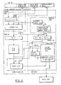
- the digital computer system sends an instruction to the instruction register (IR) 10 and a first storage means stores the instruction in the IR 10.
- the first storage means is a latch or similar standard type device for securely defining when the instruction is stored.
- the instruction is typically one of several instructions from a stack of instructions stored in the computer and sequentially sent to the instruction register for process-ing.
- the instruction is made up of a concatenated series of bits. It is also broken up into two parts, an operator part and operand part. The high order bits of thee instruction are assigned to the operator part of the instruction.
- the instruction is decoded and the decoded operator part re-quests the arithmetic logic unit (ALU) 500 to perform some type of function.
- ALU arithmetic logic unit
- the operand part of the instruction contains the address information indicating the location of the data, requested by the operand, within the memory or storage system of the comput-er.
- the operand of the instruction is a series of bits that is divided into three sections and two of the sections specify a register within the computer which holds informa-tion to be used in generating a desired address of data within cache memory.
- the third section is itself used in the generation of the desired address.
- the high order bits specify an index register and the middle group of bits specify a base register.
- the index and base registers are part of the general purpose registers (GPRs) 320 of the computer.
- the lower order group are called displacement bits 16.
- the contents of the index register and the base register are added, by an adder 310 to the displacement bits 16 to produce a virtual address.
- the virtual address is placed in the virtual address register (VAR) 40 and is used to index a table, called the translation look aside buffer (TLB) 420, which contains the desired or real address of the data in cache memory.
- VAR virtual address register
- TLB translation look aside buffer
- the cache memory access system 5 will determine, after the instruction is decoded, whether the data requested is within the cache memory 410 of the computer.
- the data is typically accessed as a group of data bits, designated as a word.
- the cache memory access system 5 will retrieve the data to be used by the ALU 500 on the machine cycle following the decode of the instruction.
- the ALU 500 will receive the data from a main storage access system, which is beyond the scope of this application.
- the cache memory access system 5 is divided into two parts, an access part and a verification part.
- the access part includes the cache directory 430, the cache memory means 400, and the ALU 500.
- the access part directly retrieves the data from the cache memory 410, through the use of a predicted address generation means 200.
- the verification part guarantees that the data retrieved by the cache memory is the data that was requested by the instruction.
- the verification part includes a virtual address generation means 300, a translation look aside buffer (TLB) 420, and a comparison means 440 to compare a predicted real address (generated by the access part of the cache system) with the real address generated by the TLB 420 within the verification part.
- TLB translation look aside buffer
- the cache memory array 410 is divided into 512 congru-ence classes of 4 lines each, and each line contains 128 bytes of data which results in a 256K byte cache memory array.
- One line of all the congruence classes form a set, and therefore the memory is accessed by choosing the bits that correspond to a set, a congruence class, and byte within a line.
- the predicted real address generation means (PRAGM) 200 chooses the bits associated with the set, part of the congruence class, and an address tag to retain identification of the address. These 19 bits form the high order portion of the predicted real address and are placed in the high order part of the predicted real address regis-ter (PRAR) 30.
- the virtual address generation means (VAGM) 300 generates a virtual address, and a portion, 12 bits (page offset bits), of that virtual address contains the bits associated with the data byte within the line and part of the congruence class. These bits form the low order portion of the predicted real address and are placed in the low order portion of the predicted real address register (PRAR) 30. Both the predicted real address generation means and the virtual address generation means place the results in the 30 during the instruction decode machine cycle.
- the cache memory means (CMM) 400 subsequently retrieves the data from the location, within the cache memory array 410, of the predicted real address which is in the PRAR 30. The retrieval of the data is performed on the machine cycle following the instruction decode cycle, also called the cache access machine cycle.
- the cache memory access system 5 verifies that the predicted real address is the address required by the instruction. This verification is accomplished by generating a virtual ad-dress, through a virtual address generation means (VAGM) 300, during the instruction decode machine cycle.
- VAGM virtual address generation means
- the virtual address is placed in a virtual address register (VAR) 40, and the contents of that register are subsequently compared against entries in a translation look aside buffer (TLB) 420.
- the TLB 420 contains potential addresses that are generated by the VAGM 300, and the corresponding real addresses (actual addresses required by the instruction) for each potential virtual address.
- the TLB 420 selects the real address corresponding to the matched potential virtual address.
- the selection of the real ad-dress, corresponding to the virtual address, from the entries in the TLB 420 is accomplished during the cache access machine cycle.
- the real address, selected by the TLB 420, is subse-quently sent to a comparison means, within the CMM 400.
- the comparison means of the 400 is for comparing the pre-dicted real address in the 30 to the real address generated by the TLB 420.
- the comparison means compares the two addresses bit by bit to determine whether the addresses are identical.
- the comparison of the predicted real address to the real address is accomplished during the cache access machine cycle after the real address selection in the TLB 420.
- the comparison of the real address to the predicted real address provides the verification of the predicted real address used to access the cache memory array during the cache access machine cycle.
- the CMM 400 retrieves the data and sends it to the ALU 500 for execution after the cache access machine cycle.
- the CMM 400 When the comparison is not a match, the CMM 400 will retrieve data from the location, within the cache memory array 410, of the real address obtained from the TLB 420. The CMM 400 re-trieves the data from the real address of the TLB on the machine cycle following the cache access machine cycle. Once the CMM 400 has retrieved the data from the real address of the TLB 420, the CMM 400 sends the data to the ALU 500 for execution.
- the CMM 400 has a receiving means not shown, which receives the real address or the predicted real address.
- the CMM 400 performs the same function regardless of the type (predicted or real) of address sent to the CMM 400.
- the receiving means compares the received address to addresses contained within a cache directory 430.
- the cache directory contains 512 congruence classes which correspond to 2K real addresses entered into the directory.
- the congruence class is identified by an identical 9 bit part of the four real addresses contained within each congruence class.
- the receiving means compares the 9 bit part of the four real addresses in the directory 430 with a correspond-ing 9 bit part of the received address. Then the receiving means compares the four address values selected in the directory with the received (real or predicted real) address to determine which set the received address is contained in.
- the cache memory While the receiving means is determining which set the received address is in, the cache memory is being accessed by part of the received address.
- the cache memory has a retrieval means which retrieves data within all the address-es associated within one congruence class.
- the retrieval means accesses all four data locations while the directory is determining which of four possible sets the data actually resides in. This is done by accessing the first 16 bits of the 256K addresses. This 16 bits includes the 9 bit congru-ence class information and 7 bits of byte address within each element of the congruence class.
- the retrieval means selects the correct data for the received (real or predicted real) address.
- the selection signal sent to the retrieval means which contains a selection means 415, determines which of the four bytes of data to select. The selection is made on the machine cycle following the cache access cycle and the selection signal is sent independently from the four addresses sent by the receiving means to the retrieval means.
- the selected data is sent to the ALU 500 which uses it in executing a function on the second machine cycle after the cache access machine cycle.
- the CMM 400 receives the predicted real address from the 30, which in turn, had received bits comprising the predicted real address from the PRAGM 200 and the VAGM 300.
- the PRAGM 200 generates the bits for the PRAR 30 from a history table 21a.
- the history table 210 stores a number of the most recent real addresses (128 addresses here) called for by recent instructions along with the corresponding content of the base register specified in the instruction register.
- the PRAGM 200 compares the content of the base register specified in the IR 10 with the most recently used base register contents stored in the history table 210, which were saved after being used.
- the 19 bits stored in the history table 210 are stored in the high order portion of the PRAR 30 by a third storage means.
- the third storage means is a latch or similar type device for transferring data into a register.
- These 19 high order bits contain an address tag as well as the bits associated with the set selection and 4 of 9 of the congruence class bits associated with the predicted real address.
- the VAGM 300 generates the bits associated with the predicted real address through an adder 310 and general purpose registers (GPRs) 320.
- the adder 310 is a means for adding the three parts of the address specified in the IR 10.
- the addition of the displacement bits with the content of the base register and the content of the index register, specified in the IR 10, generates the 31 bit virtual address placed in the virtual address register (VAR) 40.
- the virtual address' low order 12 bits are the page offset bits and the next 6 higher order bits are the virtual address page address bits.
- the adder 310 receives the instruction register (current address) displacement bits directly from the IR 10, the adder 310 receives the content of the base register and index register from the GPRs 320.
- the PRAGM also receives the content of the base register, which is a general purpose register (GPR).
- the adder resolves the 12 low order bits first which also correspond to all 7 bits choosing the byte within a line and 5 of the 9 bits associ-ated with the choice of the congruence class. These 12 bits are sent to the PRAR 30 and a second storage means stores the bits in the low order portion of the predicted real address.
- the second storage means is a standard latch or similar standard device for transferring data into register.
- the efficient operation of the cache access system 5 requires that the history table 210 have the most recently used real addresses and the corresponding base register contents. This is accomplished through a history table update in the cache access system 5.
- an update means updates the history table 210. This is because such a condition means that the last predicted address was incor-rect and therefore the value generated from the history table 210 was incorrect.
- the PRAGM 200 has found an entry in the history table 210 in which the content of the base register specified by the IR 10 matches a history table entry but the corresponding real address does not match the address given by the TLB 420.
- the corresponding real address in the history table is updated to reflect the real address generated by the TLB 420.
- the second situation requiring a history table update is when none of the entries in the history table 210 match the content of the base register. In this situation the least recently used entry in the history table 210 is replaced with the content of the base register specified in the IR 10 and the corresponding real address generated by the TLB 420.
- the above method of updating the history table 210 assumes that the history table 210 is fully associative, that is contains only one set.
- history table 210 is set associative, containing several sets, then when no match is found between the contents of the base register and the history table 210, the least recently used entry of the set selected by the partial content of the base register is replaced rather than the least recently used entry in the entire history table 210.
- This embodiment of the disclosed invention accesses the cache memory array 410 with two separate addresses.
- the first is the predicted real address which is a "best guess" of the location of data that the instruction requires. This guess is generated by a history table 210 and an adder 310.
- the history table 210 lists real address and their corre-sponding base register contents from the GPRs 320.
- the history table 210 matches a recently used base register content from the list of recently used base register con-tents, to the content of the current base register specified in the IR 10.
- the history table 210 selects the real address that corresponds to that recently used base register content and places it in the high order bits of the PRAR 30.
- the adder 310 adds the content of the current base register, content of the index register, and the displacement bits from the IR 10, and places those 31 bits in the VAR 20. It also takes the low order 12 bits from the adder, which are resolved earliest, and places them in the low order 12 bits of the PRAR 30. The 31 bits in the PRAR are then used to access the cache array. When the "guess" is right the cache memory sends the data to the ALU 500 to be executed. When the guess is wrong a real address, generated from the TLB 210, is used to access the cache array.
- the guess from the PRAR 30 is verified by comparing, in a comparison means 425, the predicted real address with the real address generated by the TLB 210. This comparison is accomplished while the cache array is retrieving the data in the predicted real address location.
- the real address is generated by matching the virtual address in the VAR 40 with entries in the TLB, which contains possible virtual address-es to be generated by the VAGM 300 and the corresponding real addresses. When the virtual address in the VAR 40 does not match the entries in the TLB 420, a process must be initiated to compile the corresponding real address. This is a conventional step in virtual memory machines and beyond the scope of this application.
- the data sent to the ALU 500 is delayed one machine cycle when the "guess" is wrong because the memory has to be re-accessed with the real address after the memory array has been accessed with the incorrect "guess" (predicted real) address.
- the incorrect guesses are minimized by updating the history table 210 with new current addresses and corresponding real addresses from the TLB 420.
- the history table is updated when guesses are determined to be incorrect.
- a current address which is already in the history table merely has its real address replaced, while a current address that is not in the history table, when the history table is to be updated, replaces an existing current instruction and its corresponding real address.
- FIG. 3 An alternate embodiment of this invention is shown in Figure 3. This embodiment is similar to the first embodi-ment except that the PRAGM 200 also comprises a translation look ahead table (TLAT) 220.
- the TLAT 220 is a smaller history table that has a recently used real address entry for each GPR available in the computer system, there are 16 in the present invention.
- 19 bits associated with the recently used real address entry of the TLAT 220, corresponding to the specified base register are placed in the high order positions of the PRAR 30.
- This is shown in Figure 3 by having the four bit base register identifier also specify the TLAT 220 entry. These 19 bits are concatenated with the 12 bit page offset bits (placed in the low order portions of the PRAR 30) from the adder 310 to form the predicted real address in the PRAR 30.
- the larger history table 210 is used to update the TLAT 220 on every machine cycle.
- the TLAT requires an array which can be read from and written to within the duration of the decode machine cycle so that it can be updated during that cycle.
- the new content of this affect-ed GPR is used to retrieve the corresponding predicted real address entry in the history table 210.
- This predicted real address is then used to replace the entry in the TLAT 220 corresponding to this GPR.
- the update process of the history table 220 is similar to the process described in the first embodiment.
- the predicted real address does not match the real address from the TLB 420, the history table must be updated with the real address from the TLB 420.
- the TLAT 220 must also be updated, similar to above described process, to reflect the changes in the history table 210.
- the TLAT 220 essentially acts as a window into the larger history table 210. Since a machine can only have fixed set of GPRs 320 and the TLAT 220 always has a predict-ed real address entry for each GPR, this technique can predict the real addresses with the same accuracy as the approach described in the first embodiment regardless of which GPR is used as the current base register. Additionally, the TLAT is a very small array and its access can be done in parallel with the GPR access which makes access to the array very fast. Therefore, the dual table approach (TLAT and history table) as described in this embodiment provides a faster way to predict real addresses than the technique described in the first embodiment with the same accuracy.
- cache memory access system that increases the speed with which an address can be accessed. This is achieved by shortening the machine cycles of the computer associated with the cache memory.
- the described cache memory access system avoids the synonym problem associated with set associative cache memories.
- the address accessed in response to an instruction is predicted based on only a part of the address selected by the instruction.
- the predicted address is generated quickly and with a low level of incorrect predictions, and is verified while the cache memory is retrieving the data associated with the predicted real address.
- the verification of the predicted real address is based on a virtual address which in turn is used to access a table of correct real addresses.
- the source of the predicted real address is updated to minimize the frequency of incorrect predicted real addresses.
Landscapes
- Engineering & Computer Science (AREA)
- Theoretical Computer Science (AREA)
- Software Systems (AREA)
- Physics & Mathematics (AREA)
- General Engineering & Computer Science (AREA)
- General Physics & Mathematics (AREA)
- Memory System Of A Hierarchy Structure (AREA)
Applications Claiming Priority (2)
| Application Number | Priority Date | Filing Date | Title |
|---|---|---|---|
| US424496 | 1989-10-20 | ||
| US07/424,496 US5148538A (en) | 1989-10-20 | 1989-10-20 | Translation look ahead based cache access |
Publications (2)
| Publication Number | Publication Date |
|---|---|
| EP0424163A2 true EP0424163A2 (fr) | 1991-04-24 |
| EP0424163A3 EP0424163A3 (en) | 1991-12-04 |
Family
ID=23682835
Family Applications (1)
| Application Number | Title | Priority Date | Filing Date |
|---|---|---|---|
| EP19900311473 Withdrawn EP0424163A3 (en) | 1989-10-20 | 1990-10-18 | Translation look ahead based cache access |
Country Status (3)
| Country | Link |
|---|---|
| US (1) | US5148538A (fr) |
| EP (1) | EP0424163A3 (fr) |
| JP (1) | JPH03194632A (fr) |
Cited By (6)
| Publication number | Priority date | Publication date | Assignee | Title |
|---|---|---|---|---|
| EP0581425A1 (fr) * | 1992-06-30 | 1994-02-02 | Sun Microsystems, Inc. | Recouvrement rapide de données d'une structure mémoire de données avec annotations prédictives d'un accès précédent |
| EP0652521A1 (fr) * | 1993-11-04 | 1995-05-10 | Sun Microsystems, Inc. | Recouvrement rapide de données d'une structure mémoire de données adressée physiquement avec annotation prédictives de franchissement de frontières de pages |
| WO2014100653A1 (fr) * | 2012-12-20 | 2014-06-26 | Qualcomm Incorporated | Adressage spéculatif utilisant une mémoire tampon de croisement de pages d'une adresse virtuelle à une adresse physique |
| EP4020228A1 (fr) * | 2020-12-23 | 2022-06-29 | Intel Corporation | Dispositif, système et procédé de retrait sélectif d'instructions de prélecture de logiciel |
| WO2024030707A1 (fr) * | 2022-08-01 | 2024-02-08 | Qualcomm Incorporated | Utilisation d'historique de pages retirées pour prélecture de répertoire de pages actives (tlb) d'instructions dans des dispositifs basés sur processeur |
| US12579075B2 (en) | 2022-08-01 | 2026-03-17 | Qualcomm Incorporated | Using retired pages history for instruction translation lookaside buffer (TLB) prefetching in processor-based devices |
Families Citing this family (59)
| Publication number | Priority date | Publication date | Assignee | Title |
|---|---|---|---|---|
| US5247653A (en) * | 1990-08-17 | 1993-09-21 | Seagate Technology, Inc. | Adaptive segment control and method for simulating a multi-segment cache |
| JP2514292B2 (ja) * | 1991-04-25 | 1996-07-10 | インターナショナル・ビジネス・マシーンズ・コーポレイション | オペランドペ―ジメモリ及び命令ペ―ジメモリを有するコンピュ―タシステム |
| JPH0546475A (ja) * | 1991-08-15 | 1993-02-26 | Fujitsu Ltd | バツフア記憶制御方式 |
| WO1993018459A1 (fr) * | 1992-03-06 | 1993-09-16 | Rambus Inc. | Preextraction dans un cache afin de reduire au minimum le temps d'acces a la memoire centrale et la taille du cache dans un systeme informatique |
| US5392410A (en) * | 1992-04-30 | 1995-02-21 | International Business Machines Corporation | History table for prediction of virtual address translation for cache access |
| US5418922A (en) * | 1992-04-30 | 1995-05-23 | International Business Machines Corporation | History table for set prediction for accessing a set associative cache |
| US5361391A (en) * | 1992-06-22 | 1994-11-01 | Sun Microsystems, Inc. | Intelligent cache memory and prefetch method based on CPU data fetching characteristics |
| JP3199465B2 (ja) * | 1992-07-22 | 2001-08-20 | 株式会社日立製作所 | 情報処理装置 |
| JPH0659972A (ja) * | 1992-08-05 | 1994-03-04 | Oki Electric Ind Co Ltd | メモリ制御装置 |
| GB2270791B (en) * | 1992-09-21 | 1996-07-17 | Grass Valley Group | Disk-based digital video recorder |
| US5442766A (en) * | 1992-10-09 | 1995-08-15 | International Business Machines Corporation | Method and system for distributed instruction address translation in a multiscalar data processing system |
| US5386534A (en) * | 1992-10-27 | 1995-01-31 | Motorola, Inc. | Data processing system for generating symmetrical range of addresses of instructing-address-value with the use of inverting sign value |
| US5651130A (en) * | 1993-03-22 | 1997-07-22 | Compaq Computer Corporation | Memory controller that dynamically predicts page misses |
| US5422837A (en) * | 1993-12-14 | 1995-06-06 | Bull Hn Information Systems Inc. | Apparatus for detecting differences between double precision results produced by dual processing units operating in parallel |
| JPH07287668A (ja) | 1994-04-19 | 1995-10-31 | Hitachi Ltd | データ処理装置 |
| US5890221A (en) * | 1994-10-05 | 1999-03-30 | International Business Machines Corporation | Method and system for offset miss sequence handling in a data cache array having multiple content addressable field per cache line utilizing an MRU bit |
| US5933860A (en) * | 1995-02-10 | 1999-08-03 | Digital Equipment Corporation | Multiprobe instruction cache with instruction-based probe hint generation and training whereby the cache bank or way to be accessed next is predicted |
| US5778436A (en) * | 1995-03-06 | 1998-07-07 | Duke University | Predictive caching system and method based on memory access which previously followed a cache miss |
| US6813699B1 (en) * | 1995-06-02 | 2004-11-02 | Transmeta Corporation | Speculative address translation for processor using segmentation and optional paging |
| US5987561A (en) | 1995-08-31 | 1999-11-16 | Advanced Micro Devices, Inc. | Superscalar microprocessor employing a data cache capable of performing store accesses in a single clock cycle |
| US5860104A (en) * | 1995-08-31 | 1999-01-12 | Advanced Micro Devices, Inc. | Data cache which speculatively updates a predicted data cache storage location with store data and subsequently corrects mispredicted updates |
| US5752069A (en) * | 1995-08-31 | 1998-05-12 | Advanced Micro Devices, Inc. | Superscalar microprocessor employing away prediction structure |
| US5596735A (en) * | 1996-02-23 | 1997-01-21 | Cyrix Corporation | Circuit and method for addressing segment descriptor tables |
| US5838943A (en) * | 1996-03-26 | 1998-11-17 | Advanced Micro Devices, Inc. | Apparatus for speculatively storing and restoring data to a cache memory |
| US5893930A (en) * | 1996-07-12 | 1999-04-13 | International Business Machines Corporation | Predictive translation of a data address utilizing sets of associative entries stored consecutively in a translation lookaside buffer |
| US5956752A (en) * | 1996-12-16 | 1999-09-21 | Intel Corporation | Method and apparatus for accessing a cache using index prediction |
| US5956746A (en) * | 1997-08-13 | 1999-09-21 | Intel Corporation | Computer system having tag information in a processor and cache memory |
| US6134643A (en) * | 1997-11-26 | 2000-10-17 | Intel Corporation | Method and apparatus for cache line prediction and prefetching using a prefetch controller and buffer and access history |
| US6138215A (en) * | 1998-04-30 | 2000-10-24 | International Business Machines Corporation | Method for absolute address history table synonym resolution |
| US6138223A (en) * | 1998-04-30 | 2000-10-24 | International Business Machines Corporation | Absolute address history table index generation for predicting instruction and operand cache accesses |
| US6230260B1 (en) | 1998-09-01 | 2001-05-08 | International Business Machines Corporation | Circuit arrangement and method of speculative instruction execution utilizing instruction history caching |
| US6418525B1 (en) * | 1999-01-29 | 2002-07-09 | International Business Machines Corporation | Method and apparatus for reducing latency in set-associative caches using set prediction |
| KR100343940B1 (ko) * | 1999-02-26 | 2002-07-20 | 삼성전자 주식회사 | 트랜슬레이션 룩어헤드 버퍼 예측 비트를 이용한 쓰기동작시의 캐쉬 얼리어싱 방지 |
| JP2001034537A (ja) | 1999-07-23 | 2001-02-09 | Toshiba Corp | アドレス変換回路 |
| US6425058B1 (en) | 1999-09-07 | 2002-07-23 | International Business Machines Corporation | Cache management mechanism to enable information-type dependent cache policies |
| US6412043B1 (en) | 1999-10-01 | 2002-06-25 | Hitachi, Ltd. | Microprocessor having improved memory management unit and cache memory |
| US6553460B1 (en) | 1999-10-01 | 2003-04-22 | Hitachi, Ltd. | Microprocessor having improved memory management unit and cache memory |
| US6629207B1 (en) | 1999-10-01 | 2003-09-30 | Hitachi, Ltd. | Method for loading instructions or data into a locked way of a cache memory |
| US6772325B1 (en) * | 1999-10-01 | 2004-08-03 | Hitachi, Ltd. | Processor architecture and operation for exploiting improved branch control instruction |
| US6598128B1 (en) | 1999-10-01 | 2003-07-22 | Hitachi, Ltd. | Microprocessor having improved memory management unit and cache memory |
| US6421761B1 (en) * | 1999-11-09 | 2002-07-16 | International Business Machines Corporation | Partitioned cache and management method for selectively caching data by type |
| JP3848161B2 (ja) * | 1999-12-09 | 2006-11-22 | 富士通株式会社 | アドレス変換履歴テーブルを用いたメモリアクセス装置及び方法 |
| US7707397B2 (en) * | 2001-05-04 | 2010-04-27 | Via Technologies, Inc. | Variable group associativity branch target address cache delivering multiple target addresses per cache line |
| US7310706B1 (en) | 2001-06-01 | 2007-12-18 | Mips Technologies, Inc. | Random cache line refill |
| US6745313B2 (en) * | 2002-01-09 | 2004-06-01 | International Business Machines Corporation | Absolute address bits kept in branch history table |
| US6839826B2 (en) * | 2002-02-06 | 2005-01-04 | Sandisk Corporation | Memory device with pointer structure to map logical to physical addresses |
| EP1658563B1 (fr) * | 2003-08-28 | 2013-06-05 | MIPS Technologies, Inc. | Appareil et méthode pour declenchement de flux d'instructions concurrents dans un microprocesseur a traitement multifiliere |
| US7117290B2 (en) * | 2003-09-03 | 2006-10-03 | Advanced Micro Devices, Inc. | MicroTLB and micro tag for reducing power in a processor |
| US20050050278A1 (en) * | 2003-09-03 | 2005-03-03 | Advanced Micro Devices, Inc. | Low power way-predicted cache |
| US7237098B2 (en) * | 2003-09-08 | 2007-06-26 | Ip-First, Llc | Apparatus and method for selectively overriding return stack prediction in response to detection of non-standard return sequence |
| US7328429B2 (en) * | 2003-11-13 | 2008-02-05 | Intel Corporation | Instruction operand tracing for software debug |
| US20080114940A1 (en) * | 2004-09-30 | 2008-05-15 | Renesas Technology Corp. | Data Processor |
| US9946547B2 (en) | 2006-09-29 | 2018-04-17 | Arm Finance Overseas Limited | Load/store unit for a processor, and applications thereof |
| US7594079B2 (en) * | 2006-09-29 | 2009-09-22 | Mips Technologies, Inc. | Data cache virtual hint way prediction, and applications thereof |
| US8255634B2 (en) * | 2010-08-11 | 2012-08-28 | Lsi Corporation | Apparatus and methods for look-ahead virtual volume meta-data processing in a storage controller |
| US8176218B2 (en) | 2010-08-11 | 2012-05-08 | Lsi Corporation | Apparatus and methods for real-time routing of received commands in a split-path architecture storage controller |
| US8261003B2 (en) | 2010-08-11 | 2012-09-04 | Lsi Corporation | Apparatus and methods for managing expanded capacity of virtual volumes in a storage system |
| US10275256B2 (en) * | 2016-02-22 | 2019-04-30 | International Business Machines Corporation | Branch prediction in a computer processor |
| US10579522B2 (en) | 2016-09-13 | 2020-03-03 | Andes Technology Corporation | Method and device for accessing a cache memory |
Family Cites Families (9)
| Publication number | Priority date | Publication date | Assignee | Title |
|---|---|---|---|---|
| US4332010A (en) * | 1980-03-17 | 1982-05-25 | International Business Machines Corporation | Cache synonym detection and handling mechanism |
| US4400774A (en) * | 1981-02-02 | 1983-08-23 | Bell Telephone Laboratories, Incorporated | Cache addressing arrangement in a computer system |
| JPS57143782A (en) * | 1981-03-03 | 1982-09-06 | Toshiba Corp | Information processor |
| US4441155A (en) * | 1981-11-23 | 1984-04-03 | International Business Machines Corporation | Page controlled cache directory addressing |
| JPS60123946A (ja) * | 1983-12-09 | 1985-07-02 | Hitachi Ltd | アドレス変換装置 |
| US4737909A (en) * | 1985-04-01 | 1988-04-12 | National Semiconductor Corp. | Cache memory address apparatus |
| US4785398A (en) * | 1985-12-19 | 1988-11-15 | Honeywell Bull Inc. | Virtual cache system using page level number generating CAM to access other memories for processing requests relating to a page |
| US4774659A (en) * | 1986-04-16 | 1988-09-27 | Astronautics Corporation Of America | Computer system employing virtual memory |
| US4757447A (en) * | 1986-07-28 | 1988-07-12 | Amdahl Corporation | Virtual memory system having identity marking for common address space |
-
1989
- 1989-10-20 US US07/424,496 patent/US5148538A/en not_active Expired - Fee Related
-
1990
- 1990-09-20 JP JP2251670A patent/JPH03194632A/ja active Granted
- 1990-10-18 EP EP19900311473 patent/EP0424163A3/en not_active Withdrawn
Cited By (10)
| Publication number | Priority date | Publication date | Assignee | Title |
|---|---|---|---|---|
| EP0581425A1 (fr) * | 1992-06-30 | 1994-02-02 | Sun Microsystems, Inc. | Recouvrement rapide de données d'une structure mémoire de données avec annotations prédictives d'un accès précédent |
| EP0652521A1 (fr) * | 1993-11-04 | 1995-05-10 | Sun Microsystems, Inc. | Recouvrement rapide de données d'une structure mémoire de données adressée physiquement avec annotation prédictives de franchissement de frontières de pages |
| US5548739A (en) * | 1993-11-04 | 1996-08-20 | Sun Microsystems, Inc. | Method and apparatus for rapidly retrieving data from a physically addressed data storage structure using address page crossing predictive annotations |
| WO2014100653A1 (fr) * | 2012-12-20 | 2014-06-26 | Qualcomm Incorporated | Adressage spéculatif utilisant une mémoire tampon de croisement de pages d'une adresse virtuelle à une adresse physique |
| JP2016505972A (ja) * | 2012-12-20 | 2016-02-25 | クアルコム,インコーポレイテッド | 仮想アドレス−物理アドレスページクロスバッファを用いた推測的なアドレッシング |
| US9804969B2 (en) | 2012-12-20 | 2017-10-31 | Qualcomm Incorporated | Speculative addressing using a virtual address-to-physical address page crossing buffer |
| EP4020228A1 (fr) * | 2020-12-23 | 2022-06-29 | Intel Corporation | Dispositif, système et procédé de retrait sélectif d'instructions de prélecture de logiciel |
| US12111772B2 (en) | 2020-12-23 | 2024-10-08 | Intel Corporation | Device, system and method for selectively dropping software prefetch instructions |
| WO2024030707A1 (fr) * | 2022-08-01 | 2024-02-08 | Qualcomm Incorporated | Utilisation d'historique de pages retirées pour prélecture de répertoire de pages actives (tlb) d'instructions dans des dispositifs basés sur processeur |
| US12579075B2 (en) | 2022-08-01 | 2026-03-17 | Qualcomm Incorporated | Using retired pages history for instruction translation lookaside buffer (TLB) prefetching in processor-based devices |
Also Published As
| Publication number | Publication date |
|---|---|
| EP0424163A3 (en) | 1991-12-04 |
| US5148538A (en) | 1992-09-15 |
| JPH0564816B2 (fr) | 1993-09-16 |
| JPH03194632A (ja) | 1991-08-26 |
Similar Documents
| Publication | Publication Date | Title |
|---|---|---|
| US5148538A (en) | Translation look ahead based cache access | |
| US4807110A (en) | Prefetching system for a cache having a second directory for sequentially accessed blocks | |
| JP2618175B2 (ja) | キャッシュ・アクセスのための仮想アドレス変換予測の履歴テーブル | |
| US4811215A (en) | Instruction execution accelerator for a pipelined digital machine with virtual memory | |
| US4942520A (en) | Method and apparatus for indexing, accessing and updating a memory | |
| US7493480B2 (en) | Method and apparatus for prefetching branch history information | |
| EP0088239B1 (fr) | Remplacement d'antémémoire de multiprocesseur sans contrôle de programme | |
| US6449714B1 (en) | Total flexibility of predicted fetching of multiple sectors from an aligned instruction cache for instruction execution | |
| US6560690B2 (en) | System and method for employing a global bit for page sharing in a linear-addressed cache | |
| EP0480193A2 (fr) | Mécanisme de prédiction de branchements multiprédictif | |
| EP0227892A2 (fr) | Mise à jour pour table historique de branchement dans un système de traitement en pipeline | |
| EP0243724A2 (fr) | Hiérarchie de mémoires à niveaux multiples avec mode d'adressage variable | |
| EP0394624B1 (fr) | Système de processeur à multiples séquences | |
| US6138225A (en) | Address translation system having first and second translation look aside buffers | |
| KR100335672B1 (ko) | 메모리페이지크로싱예측주석을사용하는실제주소지정데이타기억구조로부터의빠른데이타검색 | |
| JPH10232834A (ja) | キャッシュメモリを作動する方法およびコンピュータシステム | |
| US4914582A (en) | Cache tag lookaside | |
| JPH0321934B2 (fr) | ||
| US4831622A (en) | Apparatus for forcing a reload from main memory upon cache memory error | |
| JPH11203199A (ja) | キャッシュ・メモリ | |
| US5412786A (en) | Data pre-fetch control device | |
| JPWO2001042927A1 (ja) | アドレス変換履歴テーブルを用いたメモリアクセス装置及び方法 | |
| EP0173909B1 (fr) | Circuit de commande de marquage le moins recémment utilisé pour tampon à consultation parallèle | |
| US6745313B2 (en) | Absolute address bits kept in branch history table | |
| EP0206050A2 (fr) | Antémémoire à étiquettes physiques adressée virtuellement |
Legal Events
| Date | Code | Title | Description |
|---|---|---|---|
| PUAI | Public reference made under article 153(3) epc to a published international application that has entered the european phase |
Free format text: ORIGINAL CODE: 0009012 |
|
| 17P | Request for examination filed |
Effective date: 19901213 |
|
| AK | Designated contracting states |
Kind code of ref document: A2 Designated state(s): DE FR GB |
|
| PUAL | Search report despatched |
Free format text: ORIGINAL CODE: 0009013 |
|
| AK | Designated contracting states |
Kind code of ref document: A3 Designated state(s): DE FR GB |
|
| 17Q | First examination report despatched |
Effective date: 19950707 |
|
| STAA | Information on the status of an ep patent application or granted ep patent |
Free format text: STATUS: THE APPLICATION IS DEEMED TO BE WITHDRAWN |
|
| 18D | Application deemed to be withdrawn |
Effective date: 19970501 |