EP0424249A2 - Triggerimpulsgeneratorschaltung - Google Patents
Triggerimpulsgeneratorschaltung Download PDFInfo
- Publication number
- EP0424249A2 EP0424249A2 EP90402906A EP90402906A EP0424249A2 EP 0424249 A2 EP0424249 A2 EP 0424249A2 EP 90402906 A EP90402906 A EP 90402906A EP 90402906 A EP90402906 A EP 90402906A EP 0424249 A2 EP0424249 A2 EP 0424249A2
- Authority
- EP
- European Patent Office
- Prior art keywords
- input
- gate
- circuit
- signal
- mos transistor
- Prior art date
- Legal status (The legal status is an assumption and is not a legal conclusion. Google has not performed a legal analysis and makes no representation as to the accuracy of the status listed.)
- Withdrawn
Links
Images


Classifications
-
- H—ELECTRICITY
- H03—ELECTRONIC CIRCUITRY
- H03K—PULSE TECHNIQUE
- H03K5/00—Manipulating of pulses not covered by one of the other main groups of this subclass
-
- H—ELECTRICITY
- H03—ELECTRONIC CIRCUITRY
- H03K—PULSE TECHNIQUE
- H03K3/00—Circuits for generating electric pulses; Monostable, bistable or multistable circuits
- H03K3/02—Generators characterised by the type of circuit or by the means used for producing pulses
- H03K3/353—Generators characterised by the type of circuit or by the means used for producing pulses by the use, as active elements, of field-effect transistors with internal or external positive feedback
- H03K3/356—Bistable circuits
- H03K3/356104—Bistable circuits using complementary field-effect transistors
- H03K3/356113—Bistable circuits using complementary field-effect transistors using additional transistors in the input circuit
-
- H—ELECTRICITY
- H03—ELECTRONIC CIRCUITRY
- H03K—PULSE TECHNIQUE
- H03K5/00—Manipulating of pulses not covered by one of the other main groups of this subclass
- H03K5/153—Arrangements in which a pulse is delivered at the instant when a predetermined characteristic of an input signal is present or at a fixed time interval after this instant
- H03K5/1534—Transition or edge detectors
Definitions
- the present invention relates to a trigger pulse generating circuit disposed in a semiconductor integrated circuit, etc., to detect a changeover in an input signal and generate a trigger pulse.
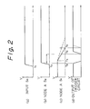
- Figure 1 shows an example of conventional trigger pulse generating circuits.
- trigger pulse generating circuit 1 has an input portion IN and an output portion OUT.
- a two-input NAND gate NG is disposed between the input and output portions.
- the two-input NAND gate NG has an output terminal connected to the output portion OUT, and input terminals 5 and 6.
- a signal processing circuit 2 is disposed between the NAND gate NG and the input portion IN to provide complementary signals S1 and S2 to the input terminals 5 and 6 of the NAND gate NG, respectively, in response to a changeover in an input signal.
- the signal processing circuit 2 includes circuits 3 and 4 to delay a drop in the signals S1 and S2 to be supplied to the input terminals 5 and 6 of the NAND gate NG.
- the signal processing circuit 2 mainly comprises MOS transistors. Signal levels of the complementary input signals S1 and S2 to be supplied to the input terminals 5 and 6 of the NAND gate NG are determined by voltages at points A and B, respectively. The voltages at the points A and B change in response to an input signal supplied to the input portion IN.
- the input signal to the input portion IN is supplied, on the one hand, directly to MOS transistors Q6 and Q7, and on the other hand, to MOS transistors Q1 and Q3 via an inverter IVT.
- a MOS transistor Q5 is turned OFF, and a MOS transistor Q8 ON.
- the MOS transistor Q6 is turned OFF, and the MOS transistor Q7 is turned ON. Namely, the MOS transistors Q7 and Q8 are conductive, while the MOS transistors Q5 and Q6 are in an OFF state. As a result, a current flows from the point B through the MOS transistors Q7 and Q8 and a resistor R2 toward a ground GND, thereby decreasing the potential at the point B as shown in Fig. 2(c).
- the signal processing circuit 2 of the trigger pulse generating circuit 1 produces the two complementary signals S1 and S2, which are provided to the NAND gate NG.
- the NAND gate NG then generates a trigger pulse in response to levels of the signals S1 and S2. More precisely, each of the signals S1 and S2 to be provided to the NAND gate NG has a delay in a rise time (from L to H) and in a fall time (from H to L), wherein the fall time is longer than the rise time. Based on the difference of the delays, a trigger pulse is generated.
- a voltage at the point A i.e., a voltage of the signal S2 changes from L to H at time t2 that is slightly delayed from the time t1 as shown in Fig. 2(b).
- a voltage at the point B i.e., a voltage of the signal S1 starts to fall from H to L at time t4 as shown in Fig. 2(c).
- a threshold of the NAND gate NG is set to an H level, usually one half of Vcc. According to the threshold, an output of the NAND gate falls at the time t2 when the potential of the point A reaches 1/2 H. Also, the output of the NAND gate rises at the time t5 when the potential of the point B becomes 1/2 H or smaller.
- a time period td between the time t3 and the time t5 is used as the width of a trigger pulse.
- the conventional trigger pulse generating circuit controls a fall time of one of the signals S1 and S2 to adjust the width of a trigger pulse.
- Supposing a fall waveform at the point B is as indicated with a dotted line in Fig. 2, the level of the signal S1 becomes 1/2 H, i.e., 1/2 Vcc at time t6, so that the width td of a trigger pulse may be extended.
- the fall times of signals to be supplied to the NAND gate NG are controlled by the adjusting circuits 3 and 4 of Fig. 1, and delays of the signals are controlled by optionally changing the values of internal resistance of the MOS transistors Q3, Q4, Q7, and Q8 as well as the resistance values of the resistors R1 and R2.
- the adjusting circuits 3 and 4 involve the MOS transistors Q3, Q4, Q7, and Q8.
- the resistance of a MOS transistor changes depending on temperature. Even when the circuits 3 and 4 are designed to provide required delays, they may be affected by temperature change during use to fluctuate signal fall times at the points A and B, thereby changing the width of a trigger pulse. This may cause a malfunction.
- a time constant CR determines a signal fall time.
- a total resistance component (a component R) of the time constant CR is considered to be the internal resistance of the MOS transistor Q3 plus the internal resistance of MOS transistor Q4 plus the resistance of resistor R1, as well as the internal resistance of MOS transistor Q7 plus the internal resistance of MOS transistor Q8 plus the resistance of resistor R2.
- a component C comprises the capacitance of respective MOS transistors, floating capacitance on wires, and capacitive components connected to the input and/or output side.
- the internal resistance of a MOS transistor is intrinsically high. Since the trigger pulse generating circuit uses a plurality of MOS transistors, the internal resistance of the MOS transistors assumes a large proportion of the component R. The internal resistance of the MOS transistors is easily affected by temperature change at a rate of 0.3%deg to 0.4%/deg and by manufacturing unevenness which is rated at plus/minus 30%. In this way, the component R fluctuates in response to the manufacturing unevenness and temperature change, thereby causing the problems mentioned above.
- the resistors R1 and R2 of Fig. 1 are diffused resistors formed on the circuit. Similar to the MOS transistors, the resistance of the resistors R1 and R2 change in response to the temperature change and manufacturing unevenness. Although the changes in the resistors R1 and R2 are small compared with those occurring in the internal resistance of the MOS transistors, they may be 0.2%/deg for the temperature change and about plus/minus 10% for the manufacturing unevenness.
- the conventional trigger pulse generating circuit includes the signal fall time adjusting circuits as an element for determining the width of a trigger pulse.
- the signal fall time adjusting circuits comprise MOS transistors having a large internal resistance which is easily affected by manufacturing unevenness and temperature change.
- the internal resistance of the MOS transistors assumes a large proportion of the total resistance of the signal fall time adjusting circuits, so that the total resistance may easily change to fluctuate the width of a trigger pulse, thereby deteriorating the reliability of the trigger pulse generating circuit.
- an object of the present invention is to provide a trigger pulse generating circuit that can suppress a change occurring in the width of a trigger pulse due to a change in the internal resistance of MOS transistors that is caused by temperature change and manufacturing unevenness.
- the present invention provides a trigger pulse generating circuit for detecting a changeover in an input signal and generating a trigger pulse, comprising a signal input portion, a trigger pulse output portion, and a signal processing means disposed between the input portion and the trigger pulse output portion.
- the signal processing means comprises a complementary signal generating means for generating complementary signals in response to an input signal provided to the input portion; a two-input gate means having input terminals for receiving the complementary signals and an output terminal connected to the trigger pulse output portion; and a delay means disposed between the complementary signal generating means and the two-input gate means, for delaying at least one of the complementary signals to be provided to the two-input gate means relative to the other by a predetermined delay time.
- the signal processing means mainly comprises MOS transistors, and the delay means includes an adjusting circuit involving a bipolar transistor and a resistor.
- each of delay circuits 3 and 4 for delaying fall times or rise times of the complementary signals to be supplied to the two-input gate includes an adjusting circuit comprising a bipolar transistor having small internal resistance and a resistor that are connected to each other in series.
- the fall times or the rise times of the signals to be supplied to the two-input gate are less affected by temperature change and manufacturing unevenness of the MOS transistors.
- the width of a trigger pulse will not fluctuate due to the temperature change, etc., thereby improving the reliability of the trigger pulse generating circuit.
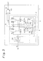
- a trigger pulse generating circuit 1 of the present invention basically comprises a signal input portion IN, a trigger pulse output portion OUT, and a signal processing means 2 disposed between the signal input portion IN and the trigger pulse output portion OUT.
- the signal processing means 2 comprises a complementary signal generating means CM for generating complementary signals S1 and S2 in response to an input signal provided to the signal input portion IN, a two-input gate means NG having input terminals 5 and 6 for receiving the complementary signals S1 and S2, respectively, and an output terminal 10 connected to the trigger pulse output portion OUT, and delay means 3 and 4 disposed between the complementary signal generating means CM and the two-input gate means NG, for delaying at least one of the complementary signals S1 and S2 to be provided to the input terminals 5 and 6 of the two-input gate means NG relative to the other by a predetermined time period.
- Essential parts of the signal processing means 2 comprise MOS transistors Q3, Q4, Q9, Q7, Q8, and Q10.
- the delay means 3 and 4 include adjusting circuits 12 and 13, respectively, that comprise bipolar transistors Q11 and Q12 and resistors R1 and R2.
- the complementary signal generating means CM comprises an inverter.
- the means CM may be any known complementary signal generating means.
- the delay means 3 and 4 delay the rise times or the fall times of the complementary signals S1 and S2, respectively. According to the present invention, it is also allowed to delay the rise time or the fall time of at least one of the complementary signals S1 and S2. In this case, either one of the delay means 3 or 4 may be omitted.
- the two-input gate means NG is a NAND gate.
- This gate means may also be a NOR gate.
- This example includes delay circuits 3 and 4 that incorporate adjusting circuits 12 and 13, respectively.
- a NAND gate NG is disposed between an input portion IN and a trigger pulse output portion OUT.
- the NAND gate NG has an output terminal connected to the trigger pulse output portion OUT.
- a signal processing circuit 2 is disposed between the NAND gate NG and the signal input portion IN, and connected to input terminals 5 and 6 of the NAND gate NG. The signal processing circuit 2 supplies a first signal to one of the input terminals 5 and 6 of the NAND gate NG, and a second signal to the other a predetermined time after the supply of the first signal.
- An input signal S0 is supplied to the input portion IN and then to a gate of a MOS transistor Q9.
- the MOS transistor Q9 is one of three N-channel MOS transistors Q3, Q4, and Q9 that are connected in series on the drain side of a P-channel MOS transistor Q1.
- a source of the MOS transistor Q1 is connected to a high-voltage power source Vcc.
- the input signal S0 is also supplied to gates of MOS transistors Q6 and Q7, which are among N-channel MOS transistors Q7, Q8, and Q10 that are connected in series on the drain side of a P-channel MOS transistor Q6.
- the source of the MOS transistor Q6 is connected to the high-voltage power source Vcc.
- the input signal S0 is passed through an inverter IVT and supplied to gates of the MOS transistors Q1 and Q3 as well as a gate of the MOS transistor Q10.
- P-channel MOS transistors Q2 and Q5 are disposed in parallel with the MOS transistors Q1 and Q6 and connected to the high-voltage power source Vcc and the sources of the MOS transistors Q3 and Q7.
- the gate of the P-channel MOS transistor Q2 forms a point B, which is connected to the input terminal 5 of the NAND gate NG.
- the point B is also connected to the gate of the MOS transistor Q4.
- the gate of the P-channel MOS transistor Q5 forms a point A, which is connected to the input terminal 6 of the NAND gate NG.
- the point A is also connected to the gate of the MOS transistor Q8.
- the source of the MOS transistor Q3 is connected to the gate of the MOS transistor Q8.
- a node between the MOS transistors Q3 and Q8 is connected to the collector of a bipolar transistor Q11.
- the emitter of the bipolar transistor Q11 is grounded through a resistor R1, and the base thereof is connected to the source of the MOS transistor Q9.
- the source of the MOS transistor Q7 is connected to the gate of the MOS transistor Q4.
- a node between the MOS transistors Q7 and Q4 is connected to the collector of a bipolar transistor Q12.
- the emitter of the bipolar transistor Q12 is grounded through a resistor R2, and the base thereof is connected to the source of the MOS transistor Q10. Drains of the MOS transistors Q9 and Q10 are grounded.
- the MOS transistors Q3, Q4 and Q9, bipolar transistor Q11, and resistor R1 form the delay adjusting circuit 4.
- the MOS transistors Q7, Q8 and Q10, bipolar transistor Q12, and resistor R2 form the delay adjusting circuit 3.
- the bipolar transistors are NPN transistors. According to the present invention, they may be PNP transistors, if they match other parts of the circuit.
- the input signal S0 changes from L (LOW) to H (HIGH) at time t2 of Fig. 2(a).
- a voltage at a point C positioned at an output of the inverter IVT then changes from H to L.
- This turns ON the MOS transistor Q1 and OFF the MOS transistor Q3. Accordingly, the point A rises from L to H as shown in Fig. 2(b).
- the MOS transistor Q10 is turned OFF.
- the input signal S0 not passing through the inverter IVT turns OFF the MOS transistor Q7 and ON the MOS transistor Q7.
- the MOS transistor Q5 is in an OFF state because the point A has risen.
- the MOS transistor Q8 is turned ON due to the rise of the point A.
- the source of the MOS transistor Q10 i.e., the base of the bipolar transistor Q12 is set to H to turn ON the bipolar transistor Q12.
- a delay time of the fall of the point B can be determined by properly selecting a resistance value of the resistor R2 because the internal resistance of the bipolar transistor Q12 is very small.
- the input signal S0 not passing the inverter IVT is also supplied to the gate of the MOS transistor Q9 to turn ON the same.
- the potential of the source of the transistor Q9 then decreases to turn OFF the bipolar transistor Q11.
- the delay circuits are formed of MOS transistors and resistors as in the case of the conventional technique, respective resistance values in the delay circuits are affected by manufacturing unevenness of the transistors and resistors and by temperature change. This fluctuates a total resistance value R of the delay circuits, thereby influencing the width of a trigger pulse.
- the MOS transistors have large manufacturing unevenness, temperature dependency, and internal resistance values. The internal resistance of the MOS transistors assumes a large proportion of the total resistance R to greatly fluctuate the total resistance R.
- a maximum resistance value will be 2.4 at 100 degrees centigrade relative to a required optimum total resistance value R which is supposed to be 1 at zero degrees centigrade.
- a large change occurs in the resistance value of the conventional circuit. Namely, the resistance value of the conventional circuit changes 2.4 times between zero and 100 degrees centigrade.
- capacitance C To quickly switch an output signal, it is necessary to discharge capacitance C. To achieve this, the capacitance C must be small. If the size of each MOS transistor is reduced to reduce the capacitance C, however, a driving capacity of the transistor is also reduced. Then, the number of the transistors must be increased, thereby increasing the total resistance R.
- each of the delay circuits includes an adjusting circuit formed of a bipolar transistor and a diffused resistor, and a current is designed to mainly pass through the adjusting circuit.
- the total resistance R in the constant RC of the delay circuit of the present invention will be a sum of the internal resistance of the bipolar transistor and the resistance of the diffused resistor.
- the bipolar transistor has a large driving capacity and small internal resistance compared with those of the MOS transistor.
- the temperature dependency of the internal resistance of the bipolar transistor is similar to that of the MOS transistor, while manufacturing unevenness of the bipolar transistor is smaller than that of the MOS transistor.
- the bipolar transistor Since the bipolar transistor has a large driving capacity, the number of bipolar transistors employed by the present invention is smaller than that of the MOS transistors employed by the conventional technique. Since the bipolar transistor has small internal resistance, it occupies a small area in the delay circuit.
- the total resistance R of the delay circuit will be about 1.4 at 100 degrees centigrade relative to 1 at zero degrees centigrade.
- the delay circuits 3 and 4 of the present embodiment involve, as their essential elements, the bipolar transistors Q11 and Q12 each having a very small internal resistance compared with that of the MOS transistor.
- the internal resistance of the bipolar transistors assumes, therefore, a small proportion of the total resistance R. This can prevent the width of a trigger pulse provided by the NAND gate NG from being affected by temperature change.
- the MOS transistors Q9 and Q10 employed by the embodiment provide switching actions on the bipolar transistors Q11 and Q12.
- the trigger pulse generating circuit according to the present invention may be employed in an ATD (Address Transition Detector) circuit.
- ATD Address Transition Detector
- the ATD circuit is a circuit for generating a clock pulse in response to a detection of a change of an address signal and for contributing to a high speed operation and a reduction of power consumptions in a circuit device.
- each edge trigger circuit (ETG) provided in the ATD circuit is required to operate in high speed and to generate pulses having a constant pulse delay or pulse width regardless of a variation caused by a temperature change or a factor in a manufacturing process thereof.
- the trigger pulse generating circuit of the present invention is suitable circuit to be used in the edge trigger circuit for an ATD circuit.
- Figure 4 shows one example of a construction of an ATD circuit utilizing a trigger pulse generating circuit of the present invention as an edge trigger circuit.
- an ATD circuit 20 comprises a plurality of address inputs IN1 to INn, a plurality of edge trigger circuits 21-1 to 21-n corresponding to each one of the address inputs IN1 to INn, a plurality of PMOS transistors Q1 to Qn, an inverter 23 and a pulse width controlling circuit (PWCG) 22.
- PWCG pulse width controlling circuit
- Each of the outputs of each one of the edge trigger circuits 21-1 to 21-n is connected to a gate of each of the PMOS transistors Q1 to Qn while a source of each one of the PMOS transistors is connected to an output of the ATD circuit 20 through the inverter 23 and the pulse width controlling circuit (PWCG) 22.
- PWCG pulse width controlling circuit
- the trigger pulse generating circuit of the present invention is used for each one of the edge trigger circuits 21-1 to 21-n respectively, in the ATD circuit 20.
- the ATD circuit 20 as shown in Fig. 4 can be preferably used with an address circuit in a memory circuit in a semiconductor integrated circuit in which information are read out from and written into each one of memory cells in the memory circuit.
- the ATD circuit selects one bit line in a memory and raises a voltage of the bit line to an H (HIGH) level.
- Bit lines that are not selected in the memory are usually at an L (LOW) level. It is required to charge the selected bit line up to the H level as quickly as possible.
- the ATD circuit detects in advance that an address has been changed, and, for example, raises the voltage level of the selected bit line to an intermediate level between the L and H levels or reduces it to a voltage level close to a ground level, thereby shortening a rise time of the selected bit line or preventing erroneous operation when the output signal level is changed from H level to L level.
- This sort of ATD circuit can employ the present invention as a means for detecting whether or not the address has been changed.
- Figure 5 shows one example of a semiconductor memory circuit utilizing a ATD circuit including the trigger pulse generating circuit of the present invention.
- Fig. 5 is the semiconductor memory circuit including a PROM circuit as a memory cell 130.
- the memory circuit comprises an address buffer 121 for X direction, a decoder 122, a plurality of word drivers 123a to 123n each of which consists of a Bi-CMOS, an address buffer 124 for Y direction, a decoder 125, a plurality of bit drivers 126a to 126n, an ATD circuit 20, a memory cell portion 130, a signal compensating circuit 160, a sense amplifier 150 and an output circuit 140.
- the ATD circuit 20 detects a change of each one of the address signals and generates an ATD pulse, i.e., an inner pulse which is transmitted to the signal compensating circuit 160 and the output circuit 140.
- the memory cell portion 130 comprises a plurality of cell diodes 41a to 41n, a plurality of word lines 42-1 to 42-n, a plurality of bit lines 43-1 to 43-n and a plurality of bit-switching transistors 44a to 44n.
- the signal compensating circuit 160 comprises PMOS transistors 51 and 52, an NMOS transistor 53, clamp diodes 54 and 55 and a bipolar transistor 56.
- the signal compensating circuit 160 compensates a level of a logic signal with a clamping circuit in response to an ATD pulse.
- the sense amplifier 150 comprises transistors 61 and 62 both of which constitute a differential amplifier, an electric current source 63, a reference source 64 and a resistor 65.
- a voltage of the reference voltage source is, for example, 2.4 V.
- the output circuit 140 comprised Schottky transistors 71 to 74, a conventional transistor 75, an NMOS transistor 76, an inverter 77, Schottky diodes 78 and 79, a conventional diode 80 and resistors.
- the output circuit 140 keeps the output terminal OUT in a high impedance with respect to an output date when the ATD pulse is input thereto.
- the output circuit 140 gradually draws an current flown in this circuit to the ground under the high impedance condition so that a potential level of the output terminal is reduced smoothly.
- the potential level of the output terminal is changed to any one of H level and L level in response to the output level of the sense amplifier 150, from the level of the output terminal caused by the operation by which the current is drawn to the ground.
- high level of power source Vcc may be, for example, 5 V while low level of power source may be ground, i.e., 0 V.
- the ATD circuit 20 outputs an ATD pulse (which is active in L level) to transfer to the signal compensating circuit 160 and the output circuit 140 at a point as shown in Fig. 5.
- the bi-polar transistor 56 When the ATD pulse is input to the signal compensating circuit 160, in the circuit 160, the bi-polar transistor 56 is turned ON thereby an emitter-follower circuit, the base of which is clamped at a predetermined level from the ground, starts to operate to raise a potential level of its emitter voltage upto 2.4 V.
- the output terminal OUT is placed in a high impedance condition.
- the current flown in the output circuit is gradually drawn to the ground due to the transistor 75 having a small driving performance being turned ON, so that the potential level of the output terminal is smoothly reduced and thus the level of the output terminal is reduced to have substantially the same potential level as the ground level.
- the high impedance condition in the output terminal is eliminated and the potential level of the output terminal is set at a level defined by an output level of the sense amplifier circuit 150.
- the level of the node B is turned to H level or L level depending upon an information stored in a selected memory cell in the memory cell portion 130.
- the potential level of the node B is read by the sense amplifier 150 and transferred to the output circuit 140.
- the potential level of the output terminal can be immediately changed from a condition which is substantially the same level as the ground level to L level.
- the potential level of the output terminal can also be immediately changed from a condition which is substantially the same level as the ground level to H level.
- the current flown through the output circuit is drawn to the ground so that the output terminal has substantially the same potential level as the ground level and further the reduction of the potential level can be carried out gradually so as not to give a noise source to a ground terminal of a device.
- this memory circuit can make the output stable and prevent from operating erroneously.
Landscapes
- Physics & Mathematics (AREA)
- Nonlinear Science (AREA)
- Manipulation Of Pulses (AREA)
- Dram (AREA)
Applications Claiming Priority (2)
| Application Number | Priority Date | Filing Date | Title |
|---|---|---|---|
| JP26611289 | 1989-10-16 | ||
| JP266112/89 | 1989-10-16 |
Publications (2)
| Publication Number | Publication Date |
|---|---|
| EP0424249A2 true EP0424249A2 (de) | 1991-04-24 |
| EP0424249A3 EP0424249A3 (en) | 1992-04-15 |
Family
ID=17426490
Family Applications (1)
| Application Number | Title | Priority Date | Filing Date |
|---|---|---|---|
| EP19900402906 Withdrawn EP0424249A3 (en) | 1989-10-16 | 1990-10-16 | A trigger pulse generating circuit |
Country Status (3)
| Country | Link |
|---|---|
| EP (1) | EP0424249A3 (de) |
| JP (1) | JPH03205912A (de) |
| KR (1) | KR910008955A (de) |
Cited By (2)
| Publication number | Priority date | Publication date | Assignee | Title |
|---|---|---|---|---|
| DE4302224A1 (de) * | 1992-01-31 | 1993-08-05 | Mitsubishi Electric Corp | |
| CN108055022A (zh) * | 2017-12-08 | 2018-05-18 | 北京时代民芯科技有限公司 | 一种带抗振荡结构的rs触发器电路 |
Family Cites Families (4)
| Publication number | Priority date | Publication date | Assignee | Title |
|---|---|---|---|---|
| US4039862A (en) * | 1976-01-19 | 1977-08-02 | Rca Corporation | Level shift circuit |
| ATE14261T1 (de) * | 1980-12-22 | 1985-07-15 | British Telecomm | Elektronische taktsignalgeneratoren. |
| US4742247A (en) * | 1985-04-26 | 1988-05-03 | Advanced Micro Devices, Inc. | CMOS address transition detector with temperature compensation |
| WO1989002678A1 (en) * | 1986-07-02 | 1989-03-23 | Plessey Overseas Limited | Logic circuits |
-
1990
- 1990-10-16 JP JP2277103A patent/JPH03205912A/ja active Pending
- 1990-10-16 KR KR1019900016468A patent/KR910008955A/ko not_active Abandoned
- 1990-10-16 EP EP19900402906 patent/EP0424249A3/en not_active Withdrawn
Cited By (3)
| Publication number | Priority date | Publication date | Assignee | Title |
|---|---|---|---|---|
| DE4302224A1 (de) * | 1992-01-31 | 1993-08-05 | Mitsubishi Electric Corp | |
| US5304857A (en) * | 1992-01-31 | 1994-04-19 | Mitsubishi Denki Kabushiki Kaisha | Pulse generating circuit for semiconductor device |
| CN108055022A (zh) * | 2017-12-08 | 2018-05-18 | 北京时代民芯科技有限公司 | 一种带抗振荡结构的rs触发器电路 |
Also Published As
| Publication number | Publication date |
|---|---|
| KR910008955A (ko) | 1991-05-31 |
| JPH03205912A (ja) | 1991-09-09 |
| EP0424249A3 (en) | 1992-04-15 |
Similar Documents
| Publication | Publication Date | Title |
|---|---|---|
| US5477176A (en) | Power-on reset circuit for preventing multiple word line selections during power-up of an integrated circuit memory | |
| US4518873A (en) | Buffer circuit for driving a C-MOS inverter | |
| US4988888A (en) | CMOS output circuit with intermediate potential setting means | |
| KR0130037B1 (ko) | 동작전압의 변동에 대응 가능한 반도체집적회로의 입력버퍼회로 | |
| US4527077A (en) | Output circuit of a semiconductor device | |
| EP0497319B1 (de) | Integrierte Halbleiter-Schaltungseinheit mit Detektionsschaltung für Substrat-Potential | |
| US4873458A (en) | Voltage level detecting circuit having a level converter | |
| US7436226B2 (en) | Power-up detection circuit that operates stably regardless of variations in process, voltage, and temperature, and semiconductor device thereof | |
| US4985646A (en) | Output buffer circuit of semiconductor integrated circuit | |
| US5517142A (en) | Output buffer with a reduced transient bouncing phenomenon | |
| EP0361841A2 (de) | Logische Bicmos-Schaltung | |
| US4290119A (en) | Memory device protected against undesirable supply voltage level | |
| US4893029A (en) | Power supply noise protection circuit | |
| US4982117A (en) | Address transition detector circuit | |
| US5254885A (en) | Bi-CMOS logic circuit with feedback | |
| US5469090A (en) | Transistor circuit for holding peak/bottom level of signal | |
| JPS6237470B2 (de) | ||
| US5418477A (en) | Data output buffer pull-down circuit for TTL interface | |
| US5654926A (en) | Semiconductor memory device | |
| US5710516A (en) | Input logic signal buffer circuits | |
| US6489815B2 (en) | Low-noise buffer circuit that suppresses current variation | |
| EP0424249A2 (de) | Triggerimpulsgeneratorschaltung | |
| KR100188617B1 (ko) | 복수 범위의 전원 전압용 반도체 메모리 디바이스 | |
| JP3313383B2 (ja) | 読み出し専用記憶装置 | |
| US6353560B1 (en) | Semiconductor memory device |
Legal Events
| Date | Code | Title | Description |
|---|---|---|---|
| PUAI | Public reference made under article 153(3) epc to a published international application that has entered the european phase |
Free format text: ORIGINAL CODE: 0009012 |
|
| AK | Designated contracting states |
Kind code of ref document: A2 Designated state(s): DE FR GB |
|
| PUAL | Search report despatched |
Free format text: ORIGINAL CODE: 0009013 |
|
| AK | Designated contracting states |
Kind code of ref document: A3 Designated state(s): DE FR GB |
|
| 17P | Request for examination filed |
Effective date: 19920713 |
|
| STAA | Information on the status of an ep patent application or granted ep patent |
Free format text: STATUS: THE APPLICATION IS DEEMED TO BE WITHDRAWN |
|
| 18D | Application deemed to be withdrawn |
Effective date: 19940503 |