EP0424696A2 - Dispositif pour tester des circuits imprimées et methode de fabrication et de diagnostique. - Google Patents
Dispositif pour tester des circuits imprimées et methode de fabrication et de diagnostique. Download PDFInfo
- Publication number
- EP0424696A2 EP0424696A2 EP90118856A EP90118856A EP0424696A2 EP 0424696 A2 EP0424696 A2 EP 0424696A2 EP 90118856 A EP90118856 A EP 90118856A EP 90118856 A EP90118856 A EP 90118856A EP 0424696 A2 EP0424696 A2 EP 0424696A2
- Authority
- EP
- European Patent Office
- Prior art keywords
- conductor
- testing
- insulator
- conductor pattern
- circuit board
- Prior art date
- Legal status (The legal status is an assumption and is not a legal conclusion. Google has not performed a legal analysis and makes no representation as to the accuracy of the status listed.)
- Granted
Links
- 238000012360 testing method Methods 0.000 title claims abstract description 78
- 238000000034 method Methods 0.000 title claims abstract description 12
- 239000012212 insulator Substances 0.000 claims abstract description 59
- 239000004020 conductor Substances 0.000 claims description 109
- 238000010030 laminating Methods 0.000 claims 10
- 238000005530 etching Methods 0.000 claims 8
- 238000004519 manufacturing process Methods 0.000 abstract description 8
- 239000010410 layer Substances 0.000 description 17
- 239000000523 sample Substances 0.000 description 6
- RYGMFSIKBFXOCR-UHFFFAOYSA-N Copper Chemical compound [Cu] RYGMFSIKBFXOCR-UHFFFAOYSA-N 0.000 description 2
- 229910052802 copper Inorganic materials 0.000 description 2
- 239000010949 copper Substances 0.000 description 2
- 238000012423 maintenance Methods 0.000 description 2
- 239000000463 material Substances 0.000 description 2
- 238000012986 modification Methods 0.000 description 2
- 230000004048 modification Effects 0.000 description 2
- 239000012790 adhesive layer Substances 0.000 description 1
- 230000004075 alteration Effects 0.000 description 1
- 239000003990 capacitor Substances 0.000 description 1
- 238000004891 communication Methods 0.000 description 1
- 238000011156 evaluation Methods 0.000 description 1
- 239000011152 fibreglass Substances 0.000 description 1
- 230000002401 inhibitory effect Effects 0.000 description 1
- 238000013101 initial test Methods 0.000 description 1
- 229920003223 poly(pyromellitimide-1,4-diphenyl ether) Polymers 0.000 description 1
- 229920001721 polyimide Polymers 0.000 description 1
- 229920006395 saturated elastomer Polymers 0.000 description 1
Images

Classifications
-
- G—PHYSICS
- G01—MEASURING; TESTING
- G01R—MEASURING ELECTRIC VARIABLES; MEASURING MAGNETIC VARIABLES
- G01R31/00—Arrangements for testing electric properties; Arrangements for locating electric faults; Arrangements for electrical testing characterised by what is being tested not provided for elsewhere
- G01R31/28—Testing of electronic circuits, e.g. by signal tracer
-
- H—ELECTRICITY
- H05—ELECTRIC TECHNIQUES NOT OTHERWISE PROVIDED FOR
- H05K—PRINTED CIRCUITS; CASINGS OR CONSTRUCTIONAL DETAILS OF ELECTRIC APPARATUS; MANUFACTURE OF ASSEMBLAGES OF ELECTRICAL COMPONENTS
- H05K1/00—Printed circuits
- H05K1/02—Details
- H05K1/0266—Marks, test patterns or identification means
- H05K1/0268—Marks, test patterns or identification means for electrical inspection or testing
-
- G—PHYSICS
- G01—MEASURING; TESTING
- G01R—MEASURING ELECTRIC VARIABLES; MEASURING MAGNETIC VARIABLES
- G01R31/00—Arrangements for testing electric properties; Arrangements for locating electric faults; Arrangements for electrical testing characterised by what is being tested not provided for elsewhere
- G01R31/28—Testing of electronic circuits, e.g. by signal tracer
- G01R31/2801—Testing of printed circuits, backplanes, motherboards, hybrid circuits or carriers for multichip packages [MCP]
- G01R31/2818—Testing of printed circuits, backplanes, motherboards, hybrid circuits or carriers for multichip packages [MCP] using test structures on, or modifications of, the card under test, made for the purpose of testing, e.g. additional components or connectors
-
- H—ELECTRICITY
- H05—ELECTRIC TECHNIQUES NOT OTHERWISE PROVIDED FOR
- H05K—PRINTED CIRCUITS; CASINGS OR CONSTRUCTIONAL DETAILS OF ELECTRIC APPARATUS; MANUFACTURE OF ASSEMBLAGES OF ELECTRICAL COMPONENTS
- H05K3/00—Apparatus or processes for manufacturing printed circuits
- H05K3/46—Manufacturing multilayer circuits
- H05K3/4688—Composite multilayer circuits, i.e. comprising insulating layers having different properties
- H05K3/4691—Rigid-flexible multilayer circuits comprising rigid and flexible layers, e.g. having in the bending regions only flexible layers
-
- Y—GENERAL TAGGING OF NEW TECHNOLOGICAL DEVELOPMENTS; GENERAL TAGGING OF CROSS-SECTIONAL TECHNOLOGIES SPANNING OVER SEVERAL SECTIONS OF THE IPC; TECHNICAL SUBJECTS COVERED BY FORMER USPC CROSS-REFERENCE ART COLLECTIONS [XRACs] AND DIGESTS
- Y10—TECHNICAL SUBJECTS COVERED BY FORMER USPC
- Y10T—TECHNICAL SUBJECTS COVERED BY FORMER US CLASSIFICATION
- Y10T29/00—Metal working
- Y10T29/49—Method of mechanical manufacture
- Y10T29/49002—Electrical device making
- Y10T29/49117—Conductor or circuit manufacturing
- Y10T29/49124—On flat or curved insulated base, e.g., printed circuit, etc.
- Y10T29/49155—Manufacturing circuit on or in base
-
- Y—GENERAL TAGGING OF NEW TECHNOLOGICAL DEVELOPMENTS; GENERAL TAGGING OF CROSS-SECTIONAL TECHNOLOGIES SPANNING OVER SEVERAL SECTIONS OF THE IPC; TECHNICAL SUBJECTS COVERED BY FORMER USPC CROSS-REFERENCE ART COLLECTIONS [XRACs] AND DIGESTS
- Y10—TECHNICAL SUBJECTS COVERED BY FORMER USPC
- Y10T—TECHNICAL SUBJECTS COVERED BY FORMER US CLASSIFICATION
- Y10T29/00—Metal working
- Y10T29/49—Method of mechanical manufacture
- Y10T29/49002—Electrical device making
- Y10T29/49117—Conductor or circuit manufacturing
- Y10T29/49124—On flat or curved insulated base, e.g., printed circuit, etc.
- Y10T29/49155—Manufacturing circuit on or in base
- Y10T29/49165—Manufacturing circuit on or in base by forming conductive walled aperture in base
Definitions
- the present invention relates to an improved structure for testing a completed printed circuit board and method for fabricating same. More particularly, the present invention includes an improved structure for testing the operability of a completed circuit board using an embedded test circuit which extends past the edge of the printed circuit board and includes connectors for easy attachment to a tester.
- the invention is a simple and unique structure and method for fabricating same for testing the operability of a printed circuit board.
- a flexible circuit board which includes a test circuit is embedded within the rigid printed circuit board during its manufacture.
- the flexible board extends past the perimeter of the final main printed circuit board and contains the desirable test points for evaluating the operability of the working circuits.
- the test circuit may contain its own conductor layer having a testing conductor pattern etched thereon or it may be a main conductor layer having a testing pattern etched thereon in addition to the working conductor patterns.
- the testing operation may be performed outside of the perimeter of the main circuit board, minimizing any interference which may otherwise have occurred with components or other parts of the surfaces of the main circuit board. Since the test points on the flexible circuit are spaced from the main printed circuit board, the circuits may be evaluated at any phase during the manufacturing process. Furthermore, the present invention may be used for maintenance purposes during the life of the printed circuit board. In some applications, it may be desirable to trim the flexible board off following initial testing.
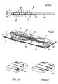
- a printed circuit board 8 having a rigid insulator 10, such as a prepregnated fiberglass sheet.
- the rigid insulator 10 supports conductor layers 12,14 which are laminated by means of an adhesive layer 13 or other bonding material to the rigid insulator 10.
- a conductor pattern 16 is etched on each conductor layer 12 and 14.
- Conductor layer 12 also has a testing pattern 18 etched on it to evaluate the operability of the principal circuit patterns 16 of each conductor layer 12 and 14 and the various devices on the circuit board 8.
- the testing pattern 18 also serves to evaluate the operability of the overall printed circuit board 8.
- Vias 20 extend from the surface of each conductor pattern and transcend the rigid insulator 10.
- the vias serve to provide electrical connections between the conductor patterns etched respectively on conductor layers 12 and 14. Attached to the top surface of each conductor layer are electrical components 22 such as logic and memory chips, resistors and capacitors. A flexible insulator 24 is attached at one edge to the rigid insulator 10.
- U.S. Patent No. 4,800,461 discloses preferred materials to use in the manufacture of the rigid and flexible insulators and their method for attachment thereto.
- the flexible insulator would be manufactured of KAPTON which is a trademark of E.I. du Pont de Nemours & Company for polyimide film.
- the conductor layer 12 is also adhered to one surface of the flexible insulator 24.
- the test pattern 18 extends past the edge of the rigid insulator 10 and continues onto the surface of the flexible insulator 24 past the edge 28 of the main printed circuit board 8.
- connection points or connectors 30 At a predetermined location past the edge of the circuit board and easily accessible during the manufacture and subsequent maintenance of the printed circuit board 8, are connection points or connectors 30.
- the connectors 30 are in electrical communication with the testing pattern 18 and permit the evaluation of the printed circuit board by contacting connectors 30 with remote probes or other robotic devices which test the quality of the board.
- Figs. 3A and 3B alternate connectors 130 and 230 are illustrated.
- the connectors as shown are copper test pads.
- the connector 130 is a pre-drilled hole having a copper lining or other conductor lining.
- the connectors may be conductive probes or pins 230 which are attached to the testing conductor pattern.
- the printed circuit board 8 may be layered in the manner shown in Fig. 4 permitting the continued stacking of rigid insulators 110 interspersed with conductor layers 113.
- the printed circuit board 108 may be expanded to multiple layers, well known to those skilled in the art, with an flexible insulator 124 attached to an interior rigid insulator as disclosed above with respect to Figs. 1 and 2. Since the insulator 124 is flexible, it may be bent easily to conserve space within the housing of the final assembled unit or may be removed entirely following the testing phases.
- the flexible insulator 224 is assembled adjacent to a rigid insulator 210.
- the printed circuit board 208 includes the rigid insulator 210 having conductor layers 213 and 214 adhered to opposite sides thereto.
- the conductor layer 213 would include the testing pattern etched thereon as well.
- Flexible insulator 224 has conductor layer 213 adhered to one said and another conductor layer 216 adhered to the opposite side. Vias 220 electrically connect the conductor patterns etched on conductor layers 213,214 and 216.
- the embodiment includes electrical components 222, such as memory chips, attached to the exposed surfaces of the printed circuit board 208.
- this embodiment may include any number of additionally stacked layers of rigid insulators 210 in combination with conductor layers to form a multilayered rigid/flex circuit in accordance with this disclosure.
- the flexible insulator 224 is the embedded flexible circuit member since it may be connected to all or any portion of any working conductor pattern by means of the vias 220.
Landscapes
- Engineering & Computer Science (AREA)
- Microelectronics & Electronic Packaging (AREA)
- General Engineering & Computer Science (AREA)
- Physics & Mathematics (AREA)
- General Physics & Mathematics (AREA)
- Computer Hardware Design (AREA)
- Printing Elements For Providing Electric Connections Between Printed Circuits (AREA)
- Production Of Multi-Layered Print Wiring Board (AREA)
- Testing Electric Properties And Detecting Electric Faults (AREA)
- Tests Of Electronic Circuits (AREA)
- Coupling Device And Connection With Printed Circuit (AREA)
- Multi-Conductor Connections (AREA)
Applications Claiming Priority (2)
| Application Number | Priority Date | Filing Date | Title |
|---|---|---|---|
| US427753 | 1989-10-26 | ||
| US07/427,753 US5001604A (en) | 1989-10-26 | 1989-10-26 | Embedded testing circuit and method for fabricating same |
Publications (3)
| Publication Number | Publication Date |
|---|---|
| EP0424696A2 true EP0424696A2 (fr) | 1991-05-02 |
| EP0424696A3 EP0424696A3 (en) | 1992-03-18 |
| EP0424696B1 EP0424696B1 (fr) | 1995-09-20 |
Family
ID=23696135
Family Applications (1)
| Application Number | Title | Priority Date | Filing Date |
|---|---|---|---|
| EP90118856A Expired - Lifetime EP0424696B1 (fr) | 1989-10-26 | 1990-10-02 | Dispositif pour tester des circuits imprimées et methode de fabrication et de diagnostique. |
Country Status (7)
| Country | Link |
|---|---|
| US (2) | US5001604A (fr) |
| EP (1) | EP0424696B1 (fr) |
| JP (1) | JPH03158777A (fr) |
| KR (1) | KR100197314B1 (fr) |
| AT (1) | ATE128245T1 (fr) |
| CA (1) | CA2025952A1 (fr) |
| DE (1) | DE69022529T2 (fr) |
Cited By (3)
| Publication number | Priority date | Publication date | Assignee | Title |
|---|---|---|---|---|
| WO1998018015A1 (fr) * | 1996-10-24 | 1998-04-30 | Ericsson Inc. | Appareil d'essai de cartes a circuit imprime |
| EP1452881A1 (fr) * | 2003-02-27 | 2004-09-01 | Pace Micro Technology Ltd | Circuit imprimé et son procédé d'utilisation |
| EP1278407A4 (fr) * | 2000-04-25 | 2005-01-05 | Matsushita Electric Works Ltd | Stratifie a couche interne contenant un circuit utilise pour la fabrication de cartes a circuit imprime multicouche pour circuit haute frequence, procede et dispositif de mesure de l'impedance du circuit dudit stratifie a couche interne contenant un circuit |
Families Citing this family (24)
| Publication number | Priority date | Publication date | Assignee | Title |
|---|---|---|---|---|
| US5001604A (en) * | 1989-10-26 | 1991-03-19 | Lusby W Randolph | Embedded testing circuit and method for fabricating same |
| US5121297A (en) * | 1990-12-31 | 1992-06-09 | Compaq Computer Corporation | Flexible printed circuits |
| US5201671A (en) * | 1992-01-24 | 1993-04-13 | Compaq Computer Corporation | Flex pull tab for surface mount connector |
| US5197889A (en) * | 1992-02-03 | 1993-03-30 | Motorola, Inc. | Electrical contact for battery package or similar device |
| US5263244A (en) * | 1992-04-17 | 1993-11-23 | Gould Inc. | Method of making a flexible printed circuit sensor assembly for detecting optical pulses |
| DE59300824D1 (de) * | 1992-12-23 | 1995-11-30 | Rheinmetall Ind Gmbh | Spannungsfeste Elektronik-Baugruppe. |
| US5363275A (en) * | 1993-02-10 | 1994-11-08 | International Business Machines Corporation | Modular component computer system |
| US5307241A (en) * | 1993-03-25 | 1994-04-26 | Northern Telecom Limited | Electronic circuit board arrangements including main auxiliary circuit boards |
| JPH06334279A (ja) * | 1993-05-20 | 1994-12-02 | Minolta Camera Co Ltd | 多層フレキシブル電装基板 |
| US5412538A (en) * | 1993-07-19 | 1995-05-02 | Cordata, Inc. | Space-saving memory module |
| JPH07306883A (ja) * | 1994-05-12 | 1995-11-21 | Fujitsu Ltd | パターン評価支援装置 |
| US5731547A (en) * | 1996-02-20 | 1998-03-24 | International Business Machines Corporation | Circuitized substrate with material containment means and method of making same |
| JP3166611B2 (ja) * | 1996-04-19 | 2001-05-14 | 富士ゼロックス株式会社 | プリント配線板及びその製造方法 |
| US6612022B1 (en) * | 1996-05-03 | 2003-09-02 | Invensys Systems, Inc. | Printed circuit board including removable auxiliary area with test points |
| KR100269947B1 (ko) * | 1997-09-13 | 2000-10-16 | 윤종용 | 인쇄회로기판및이를이용한엘씨디모듈 |
| JP2000241485A (ja) * | 1999-02-24 | 2000-09-08 | Jsr Corp | 回路基板の電気抵抗測定装置および方法 |
| DE19912441A1 (de) * | 1999-03-19 | 2000-09-21 | Elfo Ag Sachseln Sachseln | Multi-Chip-Modul |
| JP2002034126A (ja) * | 2000-07-19 | 2002-01-31 | Yazaki Corp | 配線ユニット |
| JP4830287B2 (ja) * | 2004-11-19 | 2011-12-07 | 凸版印刷株式会社 | 測定用端点付積層配線基板及びその製造方法 |
| JP2009038111A (ja) * | 2007-07-31 | 2009-02-19 | Toshiba Corp | 半導体パッケージ、プリント配線板構造および電子機器 |
| US8334704B2 (en) * | 2009-02-20 | 2012-12-18 | Apple Inc. | Systems and methods for providing a system-on-a-substrate |
| US7845956B1 (en) * | 2009-05-26 | 2010-12-07 | Thomas Baycura | Electrical component interface |
| CN102548220A (zh) * | 2010-12-29 | 2012-07-04 | 富葵精密组件(深圳)有限公司 | 电路板的制作方法 |
| TWI849804B (zh) * | 2023-03-16 | 2024-07-21 | 緯穎科技服務股份有限公司 | 電路板及電路板監控之方法 |
Family Cites Families (11)
| Publication number | Priority date | Publication date | Assignee | Title |
|---|---|---|---|---|
| US3546775A (en) * | 1965-10-22 | 1970-12-15 | Sanders Associates Inc | Method of making multi-layer circuit |
| US4540229A (en) * | 1982-04-12 | 1985-09-10 | At&T Bell Laboratories | Electrical interconnection apparatus |
| US4812792A (en) * | 1983-12-22 | 1989-03-14 | Trw Inc. | High-frequency multilayer printed circuit board |
| DE8424493U1 (de) * | 1984-08-16 | 1985-08-08 | Brumm GmbH Elektronik-Gerätebau, 1000 Berlin | Prüfadapter |
| DE3526485A1 (de) * | 1985-07-24 | 1987-02-05 | Heinz Krug | Schaltungsanordnung zum pruefen integrierter schaltungseinheiten |
| JPS62265796A (ja) * | 1986-05-14 | 1987-11-18 | 株式会社住友金属セラミックス | セラミツク多層配線基板およびその製造法 |
| US4800461A (en) * | 1987-11-02 | 1989-01-24 | Teledyne Industries, Inc. | Multilayer combined rigid and flex printed circuits |
| US5008614A (en) * | 1988-10-11 | 1991-04-16 | Hewlett-Packard Company | TAB frame and process of testing same |
| US4912401A (en) * | 1989-01-18 | 1990-03-27 | Tektronix, Inc. | Connection apparatus for interactively accessing an electronic device in a pin grid array socket |
| US5001604A (en) * | 1989-10-26 | 1991-03-19 | Lusby W Randolph | Embedded testing circuit and method for fabricating same |
| US5010446A (en) * | 1989-10-30 | 1991-04-23 | Commonwealth Edison Company | Multi-edge extender board |
-
1989
- 1989-10-26 US US07/427,753 patent/US5001604A/en not_active Expired - Lifetime
-
1990
- 1990-09-21 CA CA002025952A patent/CA2025952A1/fr not_active Abandoned
- 1990-10-02 AT AT90118856T patent/ATE128245T1/de not_active IP Right Cessation
- 1990-10-02 DE DE69022529T patent/DE69022529T2/de not_active Expired - Fee Related
- 1990-10-02 EP EP90118856A patent/EP0424696B1/fr not_active Expired - Lifetime
- 1990-10-25 KR KR1019900017102A patent/KR100197314B1/ko not_active Expired - Fee Related
- 1990-10-25 JP JP2288260A patent/JPH03158777A/ja active Pending
- 1990-11-07 US US07/610,090 patent/US5162729A/en not_active Expired - Lifetime
Cited By (3)
| Publication number | Priority date | Publication date | Assignee | Title |
|---|---|---|---|---|
| WO1998018015A1 (fr) * | 1996-10-24 | 1998-04-30 | Ericsson Inc. | Appareil d'essai de cartes a circuit imprime |
| EP1278407A4 (fr) * | 2000-04-25 | 2005-01-05 | Matsushita Electric Works Ltd | Stratifie a couche interne contenant un circuit utilise pour la fabrication de cartes a circuit imprime multicouche pour circuit haute frequence, procede et dispositif de mesure de l'impedance du circuit dudit stratifie a couche interne contenant un circuit |
| EP1452881A1 (fr) * | 2003-02-27 | 2004-09-01 | Pace Micro Technology Ltd | Circuit imprimé et son procédé d'utilisation |
Also Published As
| Publication number | Publication date |
|---|---|
| DE69022529T2 (de) | 1996-05-02 |
| US5001604A (en) | 1991-03-19 |
| KR100197314B1 (ko) | 1999-06-15 |
| EP0424696A3 (en) | 1992-03-18 |
| DE69022529D1 (de) | 1995-10-26 |
| JPH03158777A (ja) | 1991-07-08 |
| KR910008423A (ko) | 1991-05-31 |
| CA2025952A1 (fr) | 1991-04-27 |
| ATE128245T1 (de) | 1995-10-15 |
| US5162729A (en) | 1992-11-10 |
| EP0424696B1 (fr) | 1995-09-20 |
Similar Documents
| Publication | Publication Date | Title |
|---|---|---|
| US5001604A (en) | Embedded testing circuit and method for fabricating same | |
| US7096748B2 (en) | Embedded strain gauge in printed circuit boards | |
| US5399982A (en) | Printed circuit board testing device with foil adapter | |
| US6777622B2 (en) | Wiring boards | |
| EP0271692A2 (fr) | Appareil auditif miniature comportant une structure de circuit multicouche | |
| JP2755486B2 (ja) | フォイル・アダプタを有するプリント回路基板テスト装置 | |
| US5956234A (en) | Method and structure for a surface mountable rigid-flex printed circuit board | |
| JP3842267B2 (ja) | 少なくとも1つの電子部品を備えた回路基板 | |
| EP0187464B1 (fr) | Support adapteur pour circuits intégrés dépourvus de pattes de connexions | |
| WO2011075599A1 (fr) | Panneau de câblage pour le test d'une carte de circuits imprimés chargée | |
| US5798638A (en) | Apparatus for testing of printed circuit boards | |
| US6211690B1 (en) | Apparatus for electrically testing bare printed circuits | |
| US6937043B2 (en) | Apparatus and method for testing electronic component | |
| US5304922A (en) | Electrical circuit with resilient gasket support for raised connection features | |
| SE460320B (sv) | Loedfritt kopplingsdon | |
| KR20000035647A (ko) | 수직형 프로브카드 및 그것에 이용되는 기판 | |
| US20020101256A1 (en) | Detecting failures in printed circuit boards | |
| JP2000059032A (ja) | フレキシブル多層配線板 | |
| JPH01183195A (ja) | 多層印刷配線板装置の製造方法 | |
| US7094063B1 (en) | High density interconnect | |
| JP3447496B2 (ja) | 半導体搭載用配線板 | |
| JPH11326372A (ja) | コンタクトプローブおよびプローブ装置 | |
| EP0532926A1 (fr) | Circuit électrique avec un profilé élastique de support pour moyens de contact surélevés | |
| KR20260030921A (ko) | 전기적 접속 장치 | |
| JP2002181871A (ja) | プリント配線板の検査装置 |
Legal Events
| Date | Code | Title | Description |
|---|---|---|---|
| PUAI | Public reference made under article 153(3) epc to a published international application that has entered the european phase |
Free format text: ORIGINAL CODE: 0009012 |
|
| AK | Designated contracting states |
Kind code of ref document: A2 Designated state(s): AT BE CH DE ES FR GB GR IT LI NL SE |
|
| PUAL | Search report despatched |
Free format text: ORIGINAL CODE: 0009013 |
|
| AK | Designated contracting states |
Kind code of ref document: A3 Designated state(s): AT BE CH DE ES FR GB GR IT LI NL SE |
|
| 17P | Request for examination filed |
Effective date: 19920721 |
|
| 17Q | First examination report despatched |
Effective date: 19940111 |
|
| GRAA | (expected) grant |
Free format text: ORIGINAL CODE: 0009210 |
|
| AK | Designated contracting states |
Kind code of ref document: B1 Designated state(s): AT BE CH DE ES FR GB GR IT LI NL SE |
|
| PG25 | Lapsed in a contracting state [announced via postgrant information from national office to epo] |
Ref country code: IT Free format text: LAPSE BECAUSE OF FAILURE TO SUBMIT A TRANSLATION OF THE DESCRIPTION OR TO PAY THE FEE WITHIN THE PRESCRIBED TIME-LIMIT;WARNING: LAPSES OF ITALIAN PATENTS WITH EFFECTIVE DATE BEFORE 2007 MAY HAVE OCCURRED AT ANY TIME BEFORE 2007. THE CORRECT EFFECTIVE DATE MAY BE DIFFERENT FROM THE ONE RECORDED. Effective date: 19950920 Ref country code: GR Free format text: LAPSE BECAUSE OF FAILURE TO SUBMIT A TRANSLATION OF THE DESCRIPTION OR TO PAY THE FEE WITHIN THE PRESCRIBED TIME-LIMIT Effective date: 19950920 Ref country code: ES Free format text: THE PATENT HAS BEEN ANNULLED BY A DECISION OF A NATIONAL AUTHORITY Effective date: 19950920 Ref country code: BE Effective date: 19950920 Ref country code: AT Effective date: 19950920 Ref country code: NL Free format text: LAPSE BECAUSE OF NON-PAYMENT OF DUE FEES Effective date: 19950920 |
|
| REF | Corresponds to: |
Ref document number: 128245 Country of ref document: AT Date of ref document: 19951015 Kind code of ref document: T |
|
| REF | Corresponds to: |
Ref document number: 69022529 Country of ref document: DE Date of ref document: 19951026 |
|
| PGFP | Annual fee paid to national office [announced via postgrant information from national office to epo] |
Ref country code: CH Payment date: 19951031 Year of fee payment: 6 |
|
| PG25 | Lapsed in a contracting state [announced via postgrant information from national office to epo] |
Ref country code: SE Effective date: 19951220 |
|
| ET | Fr: translation filed | ||
| NLV1 | Nl: lapsed or annulled due to failure to fulfill the requirements of art. 29p and 29m of the patents act | ||
| REG | Reference to a national code |
Ref country code: CH Ref legal event code: PL |
|
| PLBE | No opposition filed within time limit |
Free format text: ORIGINAL CODE: 0009261 |
|
| STAA | Information on the status of an ep patent application or granted ep patent |
Free format text: STATUS: NO OPPOSITION FILED WITHIN TIME LIMIT |
|
| 26N | No opposition filed | ||
| PG25 | Lapsed in a contracting state [announced via postgrant information from national office to epo] |
Ref country code: CH Free format text: LAPSE BECAUSE OF FAILURE TO SUBMIT A TRANSLATION OF THE DESCRIPTION OR TO PAY THE FEE WITHIN THE PRESCRIBED TIME-LIMIT Effective date: 19961031 Ref country code: LI Free format text: LAPSE BECAUSE OF FAILURE TO SUBMIT A TRANSLATION OF THE DESCRIPTION OR TO PAY THE FEE WITHIN THE PRESCRIBED TIME-LIMIT Effective date: 19961031 |
|
| PGFP | Annual fee paid to national office [announced via postgrant information from national office to epo] |
Ref country code: GB Payment date: 19990929 Year of fee payment: 10 |
|
| PGFP | Annual fee paid to national office [announced via postgrant information from national office to epo] |
Ref country code: DE Payment date: 19991001 Year of fee payment: 10 |
|
| PGFP | Annual fee paid to national office [announced via postgrant information from national office to epo] |
Ref country code: FR Payment date: 19991011 Year of fee payment: 10 |
|
| PG25 | Lapsed in a contracting state [announced via postgrant information from national office to epo] |
Ref country code: GB Free format text: LAPSE BECAUSE OF NON-PAYMENT OF DUE FEES Effective date: 20001002 |
|
| GBPC | Gb: european patent ceased through non-payment of renewal fee |
Effective date: 20001002 |
|
| PG25 | Lapsed in a contracting state [announced via postgrant information from national office to epo] |
Ref country code: FR Free format text: LAPSE BECAUSE OF NON-PAYMENT OF DUE FEES Effective date: 20010629 |
|
| PG25 | Lapsed in a contracting state [announced via postgrant information from national office to epo] |
Ref country code: DE Free format text: LAPSE BECAUSE OF NON-PAYMENT OF DUE FEES Effective date: 20010703 |
|
| REG | Reference to a national code |
Ref country code: FR Ref legal event code: ST |