EP0424858A2 - Dispositif semi-conducteur et procédé de brasage utilisé dans sa fabrication - Google Patents
Dispositif semi-conducteur et procédé de brasage utilisé dans sa fabrication Download PDFInfo
- Publication number
- EP0424858A2 EP0424858A2 EP90120253A EP90120253A EP0424858A2 EP 0424858 A2 EP0424858 A2 EP 0424858A2 EP 90120253 A EP90120253 A EP 90120253A EP 90120253 A EP90120253 A EP 90120253A EP 0424858 A2 EP0424858 A2 EP 0424858A2
- Authority
- EP
- European Patent Office
- Prior art keywords
- plate
- plate member
- windows
- frame member
- semiconductor chip
- Prior art date
- Legal status (The legal status is an assumption and is not a legal conclusion. Google has not performed a legal analysis and makes no representation as to the accuracy of the status listed.)
- Withdrawn
Links
Images


Classifications
-
- H—ELECTRICITY
- H10—SEMICONDUCTOR DEVICES; ELECTRIC SOLID-STATE DEVICES NOT OTHERWISE PROVIDED FOR
- H10W—GENERIC PACKAGES, INTERCONNECTIONS, CONNECTORS OR OTHER CONSTRUCTIONAL DETAILS OF DEVICES COVERED BY CLASS H10
- H10W40/00—Arrangements for thermal protection or thermal control
- H10W40/20—Arrangements for cooling
- H10W40/25—Arrangements for cooling characterised by their materials
- H10W40/257—Arrangements for cooling characterised by their materials having a heterogeneous or anisotropic structure, e.g. powder or fibres in a matrix, wire mesh or porous structures
-
- H—ELECTRICITY
- H10—SEMICONDUCTOR DEVICES; ELECTRIC SOLID-STATE DEVICES NOT OTHERWISE PROVIDED FOR
- H10W—GENERIC PACKAGES, INTERCONNECTIONS, CONNECTORS OR OTHER CONSTRUCTIONAL DETAILS OF DEVICES COVERED BY CLASS H10
- H10W40/00—Arrangements for thermal protection or thermal control
- H10W40/20—Arrangements for cooling
- H10W40/25—Arrangements for cooling characterised by their materials
- H10W40/258—Metallic materials
-
- H—ELECTRICITY
- H10—SEMICONDUCTOR DEVICES; ELECTRIC SOLID-STATE DEVICES NOT OTHERWISE PROVIDED FOR
- H10W—GENERIC PACKAGES, INTERCONNECTIONS, CONNECTORS OR OTHER CONSTRUCTIONAL DETAILS OF DEVICES COVERED BY CLASS H10
- H10W70/00—Package substrates; Interposers; Redistribution layers [RDL]
- H10W70/20—Conductive package substrates serving as an interconnection, e.g. metal plates
- H10W70/24—Conductive package substrates serving as an interconnection, e.g. metal plates characterised by materials
-
- H—ELECTRICITY
- H10—SEMICONDUCTOR DEVICES; ELECTRIC SOLID-STATE DEVICES NOT OTHERWISE PROVIDED FOR
- H10W—GENERIC PACKAGES, INTERCONNECTIONS, CONNECTORS OR OTHER CONSTRUCTIONAL DETAILS OF DEVICES COVERED BY CLASS H10
- H10W76/00—Containers; Fillings or auxiliary members therefor; Seals
- H10W76/40—Fillings or auxiliary members in containers, e.g. centering rings
- H10W76/42—Fillings
- H10W76/47—Solid or gel fillings
-
- H—ELECTRICITY
- H10—SEMICONDUCTOR DEVICES; ELECTRIC SOLID-STATE DEVICES NOT OTHERWISE PROVIDED FOR
- H10W—GENERIC PACKAGES, INTERCONNECTIONS, CONNECTORS OR OTHER CONSTRUCTIONAL DETAILS OF DEVICES COVERED BY CLASS H10
- H10W90/00—Package configurations
-
- H—ELECTRICITY
- H10—SEMICONDUCTOR DEVICES; ELECTRIC SOLID-STATE DEVICES NOT OTHERWISE PROVIDED FOR
- H10W—GENERIC PACKAGES, INTERCONNECTIONS, CONNECTORS OR OTHER CONSTRUCTIONAL DETAILS OF DEVICES COVERED BY CLASS H10
- H10W72/00—Interconnections or connectors in packages
- H10W72/071—Connecting or disconnecting
- H10W72/073—Connecting or disconnecting of die-attach connectors
-
- H—ELECTRICITY
- H10—SEMICONDUCTOR DEVICES; ELECTRIC SOLID-STATE DEVICES NOT OTHERWISE PROVIDED FOR
- H10W—GENERIC PACKAGES, INTERCONNECTIONS, CONNECTORS OR OTHER CONSTRUCTIONAL DETAILS OF DEVICES COVERED BY CLASS H10
- H10W72/00—Interconnections or connectors in packages
- H10W72/071—Connecting or disconnecting
- H10W72/073—Connecting or disconnecting of die-attach connectors
- H10W72/07331—Connecting techniques
- H10W72/07336—Soldering or alloying
-
- H—ELECTRICITY
- H10—SEMICONDUCTOR DEVICES; ELECTRIC SOLID-STATE DEVICES NOT OTHERWISE PROVIDED FOR
- H10W—GENERIC PACKAGES, INTERCONNECTIONS, CONNECTORS OR OTHER CONSTRUCTIONAL DETAILS OF DEVICES COVERED BY CLASS H10
- H10W72/00—Interconnections or connectors in packages
- H10W72/30—Die-attach connectors
- H10W72/351—Materials of die-attach connectors
- H10W72/352—Materials of die-attach connectors comprising metals or metalloids, e.g. solders
-
- H—ELECTRICITY
- H10—SEMICONDUCTOR DEVICES; ELECTRIC SOLID-STATE DEVICES NOT OTHERWISE PROVIDED FOR
- H10W—GENERIC PACKAGES, INTERCONNECTIONS, CONNECTORS OR OTHER CONSTRUCTIONAL DETAILS OF DEVICES COVERED BY CLASS H10
- H10W72/00—Interconnections or connectors in packages
- H10W72/30—Die-attach connectors
- H10W72/381—Auxiliary members
-
- H—ELECTRICITY
- H10—SEMICONDUCTOR DEVICES; ELECTRIC SOLID-STATE DEVICES NOT OTHERWISE PROVIDED FOR
- H10W—GENERIC PACKAGES, INTERCONNECTIONS, CONNECTORS OR OTHER CONSTRUCTIONAL DETAILS OF DEVICES COVERED BY CLASS H10
- H10W72/00—Interconnections or connectors in packages
- H10W72/50—Bond wires
- H10W72/531—Shapes of wire connectors
- H10W72/5363—Shapes of wire connectors the connected ends being wedge-shaped
-
- H—ELECTRICITY
- H10—SEMICONDUCTOR DEVICES; ELECTRIC SOLID-STATE DEVICES NOT OTHERWISE PROVIDED FOR
- H10W—GENERIC PACKAGES, INTERCONNECTIONS, CONNECTORS OR OTHER CONSTRUCTIONAL DETAILS OF DEVICES COVERED BY CLASS H10
- H10W72/00—Interconnections or connectors in packages
- H10W72/50—Bond wires
- H10W72/551—Materials of bond wires
- H10W72/552—Materials of bond wires comprising metals or metalloids, e.g. silver
- H10W72/5524—Materials of bond wires comprising metals or metalloids, e.g. silver comprising aluminium [Al]
-
- H—ELECTRICITY
- H10—SEMICONDUCTOR DEVICES; ELECTRIC SOLID-STATE DEVICES NOT OTHERWISE PROVIDED FOR
- H10W—GENERIC PACKAGES, INTERCONNECTIONS, CONNECTORS OR OTHER CONSTRUCTIONAL DETAILS OF DEVICES COVERED BY CLASS H10
- H10W72/00—Interconnections or connectors in packages
- H10W72/50—Bond wires
- H10W72/581—Auxiliary members, e.g. flow barriers
-
- H—ELECTRICITY
- H10—SEMICONDUCTOR DEVICES; ELECTRIC SOLID-STATE DEVICES NOT OTHERWISE PROVIDED FOR
- H10W—GENERIC PACKAGES, INTERCONNECTIONS, CONNECTORS OR OTHER CONSTRUCTIONAL DETAILS OF DEVICES COVERED BY CLASS H10
- H10W72/00—Interconnections or connectors in packages
- H10W72/851—Dispositions of multiple connectors or interconnections
- H10W72/874—On different surfaces
- H10W72/884—Die-attach connectors and bond wires
-
- H—ELECTRICITY
- H10—SEMICONDUCTOR DEVICES; ELECTRIC SOLID-STATE DEVICES NOT OTHERWISE PROVIDED FOR
- H10W—GENERIC PACKAGES, INTERCONNECTIONS, CONNECTORS OR OTHER CONSTRUCTIONAL DETAILS OF DEVICES COVERED BY CLASS H10
- H10W90/00—Package configurations
- H10W90/701—Package configurations characterised by the relative positions of pads or connectors relative to package parts
- H10W90/731—Package configurations characterised by the relative positions of pads or connectors relative to package parts of die-attach connectors
- H10W90/734—Package configurations characterised by the relative positions of pads or connectors relative to package parts of die-attach connectors between a chip and a stacked insulating package substrate, interposer or RDL
-
- H—ELECTRICITY
- H10—SEMICONDUCTOR DEVICES; ELECTRIC SOLID-STATE DEVICES NOT OTHERWISE PROVIDED FOR
- H10W—GENERIC PACKAGES, INTERCONNECTIONS, CONNECTORS OR OTHER CONSTRUCTIONAL DETAILS OF DEVICES COVERED BY CLASS H10
- H10W90/00—Package configurations
- H10W90/701—Package configurations characterised by the relative positions of pads or connectors relative to package parts
- H10W90/751—Package configurations characterised by the relative positions of pads or connectors relative to package parts of bond wires
- H10W90/754—Package configurations characterised by the relative positions of pads or connectors relative to package parts of bond wires between a chip and a stacked insulating package substrate, interposer or RDL
Definitions
- the present invention relates to a semiconductor device and a soldering method for its manufacture, and particularly to improvement of a thermal stress relaxation member equipped to relax the thermal stress in a semiconductor chip and a method of soldering the semiconductor chip on a prescribed member using the improved thermal stress relaxation member.
- Fig. 6 shows a partial section showing conventional typical soldered structure of a semiconductor chip 9.
- a heat diffusion plate 1, an insulating base plate 3, an electrode plate 5 and a thermal stress relaxation plate 7 are soldered consecutively by using solder layers 2, 4 and 6.
- the semiconductor chip 9 is soldered on the thermal stress relaxation plate 7 through a solder layer 8.
- the electrode plate 5 corresponds to a collector electrode plate.
- the other electrode plates for the semiconductor chip 9, that is, an emitter electrode plate and a base electrode plate (not shown ) are connected to the semiconductor chip 9 through metallic wires 10.
- the thermal stress relaxation plate 7 is equipped in order to relax thermal stress generating within the semiconductor chip 9 during soldering process.
- the semiconductor chip 9 is made of silicon and the metallic collector plate 5 is made of copper, since coefficient of thermal expansion of the collector metallic plate 5 is around five times as much as that of the semiconductor chip 9, difference between respective shrinking is great when these are cooled from high temperature conditions in soldering. Accordingly, if the thermal stress relaxation plate 7 is not equipped, the thermal stress corresponding to this difference is directly applied to the semiconductor chip 9 to deteriorate electric characters and strength thereof. Furthermore, the thermal stress relaxation plate 7 is effective for relaxing thermal stress due to heat which is generated during electric current flow through the semiconductor chip 9.
- the thermal stress relaxation plate 7 Since the thermal stress relaxation plate 7 is provided for these reasons, the thermal stress relaxation plate 7 must be made of material of which coefficient of thermal expansion is comparatively similar to that of silicon. Besides since heat which generates during operation of the semiconductor chip 9 must be quickly transmitted to the heat diffusion plate 1, large thermal conductivity is necessary for the plate 7. Therefore, a molybdenum flat plate is widely used as a conventional thermal stress relaxation plate 7.
- the molybdenum flat plate is formed by sintering and is very high in the cost, so that the cost of the semiconductor device equipped with the structure in Fig. 6 is also high.
- a semiconductor device comprises (a) a conductive member having electric conductivity, (b) a first solder layer provided on the conductive member, (c) a composite plate member provided on the first solder layer and comprising (c-1) at least one frame member made of a first material and having a window space therein, and (c-2) a plate member made of a second material which is inserted into the window space and is unified with the frame member so that the plate member is substantially in contact with the first solder member through a first opening of the window space, (d) a second solder member provided on the composite plate member so that the composite plate member is substantially in contact with the second solder member through a second opening of the window space, and (e) a semiconductor chip provided on the second solder layer.
- the first material has a coefficient of thermal expansion equal to or less than three times a coefficient of thermal expansion of the semiconductor chip
- the second material is selected from the group consisting of copper, copper alloys, aluminum and aluminum alloys.
- the present invention also provides a thermal stress relaxation plate employable in a semiconductor device for relaxing a thermal stress in a semiconductor chip, comprising (a) at least one frame member made of a first material and having a window space therein, and (b) a plate member made of a second material which is inserted into the window space and is unified with the frame member so that the plate member has two surfaces which expose at respective window openings of the window space, wherein the first material has coefficient of thermal expansion equal to or less than three times a coefficient of thermal expansion of the semiconductor chip, and the second material is selected from the group consisting of copper, copper alloys, aluminum and aluminum alloys.
- a method of soldering a semiconductor chip on a prescribed position comprising the steps of (a) preparing a composite plate member comprising at least one frame member made of a first material and having a window space therein, and a plate member made of a second material which is inserted into the window space and is unified with the frame member so that the plate member exposes at first and second openings of the window space, wherein the first material has a coefficient of thermal expansion equal to or less than three times a coefficient of thermal expansion of the semiconductor chip, and the second material is selected from the group consisting of copper, copper alloys, aluminum and aluminum alloys, (b) soldering the composite plate member on the prescribed position while making the first opening face to the prescribed position, and (c) soldering the semiconductor chip on the composite plate member while making the semiconductor chip face to the second opening.
- the semiconductor device of the present invention either of copper, aluminum, or their alloys is used as a plate member in the composite plate member, so that thermal conductivity and electric conductivity of the composite plate member is high as a whole.
- a frame member is made of an alloy having coefficient of thermal expansion three times as high as or less than that of a semiconductor chip to suppress thermal expansion of a plate member, a relaxation effect of the whole composite plate member against thermal stress of a semiconductor chip is large.
- the composite member of the present invention can be composed without incorporating such materials as sintered molybdenum and carbon fibers, they are low in cost and usable even under high soldering temperature conditions.
- the soldering method of the present invention a semiconductor device with the above characteristics can be obtained without complicate process.
- an object of the present invention is to provide a low cost semiconductor device equipped with a thermal stress relaxation member which is high in thermal conductivity and electric conductivity and is less in restriction on a soldering temperature.
- Another object of the present invention is to provide a method of soldering a semiconductor chip for manufacturing such a semiconductor device.
- Fig. 2 and 3 are a plane view and an elevation view showing external appearance of a semiconductor device 100 according to a preferred embodiment of the present invention, respectively.
- Fig. 1 is an enlarged partial sectional view along line I-I in Fig. 2.
- the semiconductor device 100 comprises a plurality of power transistor assemblies 20 schematically shown in Fig. 3 and a casing 50 receiving these assemblies 20.
- the casing 50 has a heat diffusion plate 60 made of copper as a bottom plate on which a resin side member 70 is fixed with an adhesive agent.
- a resin lid 80 is fixed on the side member 70 so that it covers upper opening of the side member 70.
- concaves 51 are formed on the both edges of the casing 50. As shown in Fig. 1, at the bottom of each concave 51, a fitting hole 52 used for fixing the semiconductor device 100 to a desired position is provided. On the other hand, convexes 81 are provided on three positions of the lid 50. A nut 82 ( Fig. 1 ) is pressed into the convex 81, and a bolt 85 is screwed into the nut 82 through an external electrode plate 83 and a washer 84. External wires such as bus bars are connected to the external electrode plate 83 through combination of the bolt 85 and the nut 82. Though not shown in Fig. 1-3, one edge of each external electrode plate 83 is bent, and electrically connected through the lid 80 to an electrode inside the power transistor assembly 20 in the casing 50.
- Fastening terminals 87 are installed on the top of the casing 50, and a control signal for the transistor assembly 20 is applied to the fastening terminals 87, and then transmitted to a control electrode in the assembly 20 through internal wiring not shown.
- a status in which part is removed is depicted in Fig. 1, but in order to protect from outside atmosphere the transistor assemblies 20 and each internal wire, the transistor assemblies 20 are sealed with resin 51 inside an internal space of the casing 50.
- Each of the transistor assemblies 20 is manufactured as follows ( refer to Fig. 1 ) : An insulating base plate 22 made of alumina-ceramics is soldered on the heat diffusion plate 60 through a solder layer 21. A collector electrode plate 24 made of copper is soldered on the center of the upper surface of the insulating base plate 22 through a solder layer 23. On the top surface of this collector electrode plate 24, a thermal stress relaxation plate 40 is soldered through a solder layer 25. The structure of this thermal stress relaxation plate 40 will be described later in detail.
- a semiconductor chip 27 is soldered through a solder layer 26.
- the semiconductor chip 27 is formed by selectively doping impurities into a silicon substrate and is a power transistor containing junctions between a plurality of active regions.
- an emitter electrode plate 32 made of copper is soldered through a solder layer 31.
- a base electrode plate 35 made of copper is soldered on the plate 22 through a solder layer 34.
- These emitter electrode plate 32 and base electrode plate 35 are connected to an emitter region and a base region of the semiconductor chip 27 through aluminum wires 33 and 36, respectively.
- the other ones of the transistor assemblies 20 not shown in Fig. 1 also have the same structure, a plurality of the transistor assemblies 20 being connected each other through wiring and their output being led to the external electrode plates 83.
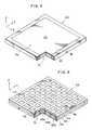
- Fig. 4 is a perspective view of the thermal stress relaxation plate 40 with part taken away.
- the thermal stress relaxation plate 40 comprises a rectangular frame member 41 and a rectangular plate member 42 inserted into a window space W1 defined by the frame member 41.
- the members 41 and 42 are united with each other to form the thermal stress relaxation plate 40.
- This thermal stress relaxation plate 40 may be obtained by rolling an assembly in which a copper plate is inserted into a rectangular invar frame. Owing to this rolling, a gap between the frame member 41 and the plate member 42 disappears, so that the members 41 and 42 are unified.
- the top and bottom surface of the thermal stress relaxation plate 40 are substantially flat, and the plate member 42 is exposed through the upper and lower openings P1 and P2 of the window space W1.
- nickel plating is applied for attaining tight soldering of the plate 40. Therefore, in case the thermal stress relaxation plate 40 is mounted as shown in Fig. 1, the plate member 42 is substantially in contact with the solder layers 25 and 26.
- thermal conductivity and coefficient of thermal expansion are shown for invar, covar, copper and silicon, respectively. Besides these values are shown also for molybdenum for comparison with conventional technology.
- the thermal conductivity of copper which is used for the plate member 42 is three times as large as that of molybdenum.
- copper is extremely high in electric conductivity. Accordingly, the thermal conductivity and the electric conductivity in an orthogonal-to-plane direction Z direction in Fig. 4 ) through the plate member 42 become extremely high in the thermal stress relaxation plate 40. Therefore, not only heat transmission during soldering is made favorable, but also transient thermal resistance during an electric current flows through the semiconductor chip becomes less. As a result, the plate 40 can be satisfactorily used for a high speed switching transistor for large power use.
- the plate member 42 is made of the same material, copper, as that of the collector electrode plate 24 and its coefficient of thermal expansion around five times as high as that of silicon, thermal stress due to difference of the coefficient of thermal expansion between the collector electrode plate 24 and the semiconductor chip 27 cannot be relaxed only by the plate member 42.
- the coefficient of thermal expansion of invar or covar which is the material of the frame member 41, is approximately the same as silicon, thermal expansion in intra-plane direction ( an X-Y direction ) of the plate member 41 can be suppressed by the frame member 41. More particularly, the coefficient of thermal expansion in the X- Y plane is around 6.0 x 10 ⁇ 6 / °C as a whole in the thermal stress relaxation plate 40.
- the thermal stress relaxation plate 42 is formed as a composite plate member consisting of the frame member 41 and the plate member 42, so that the members 41 and 42 meet the first requirement, i.e., improvement of the thermal conductivity and the electric conductivity, and the second requirement, i.e., keeping the coefficient of thermal expansion lower, respectively.
- the thermal stress relaxation plate 40 is composed as a combination of metals and alloys. Accordingly, the coupling surface between the members 41 and 42 in the thermal stress relaxation plate 40 is stable and usable at a comparatively high temperature to allow soldering with hard solder. Besides there is also no lowering of the electric conductivity due to embedding great quantity of the carbon fibers.
- Fig. 5 is a perspective view of a thermal stress relaxation plate according to another preferred embodiment of the present invention, in which part thereof is taken away.
- This thermal stress relaxation plate 43 is a composite plate member in which rectangular grid-like frame members 44 and 46 having the same configration each other are mutually arranged in parallel, and a plate material 45 is inserted between them.
- the frame members 44 and 46 are made of invar or covar, and the plate member 45 is made of copper.
- the thermal stress relaxation plate 43 may be obtained from preparing an assembly in which a copper flat plate is sandwiched between one pair of grid-like invar frames or covar frames and rolling this assembly. Each surface of the frame members 44 and 46 and the plate member 45 is nickel-plated as that of the thermal stress relaxation plate 40.
- the plate member 45 has a center portion 45a extending in an X-Y plane direction and matrix arrangements of convexes 45b and 45c projecting up-and -downward from the portion 45a, respectively.
- the convexes 45b exposes through the bottom openings Q1 and the other convexes 45c expose through the bottom openings Q2.
- the plate member 45 extends from the bottom opening Q1 of the window space W2 to the top opening Q2, so that thermal conductivity and electric conductivity in the Z direction are secured by the plate member 45 as the case of the thermal stress relaxation plate 40.
- the plate member 45 substantially contacts with the solder layers 25 and 26.
- Thermal expansion in the X-Y plane direction within the thermal stress relaxation plate 43 is limited substantially by the coefficient of thermal expansion of the flame members 44 and 46. Therefore this thermal stress relaxation plate 43 also possesses favorable properties of thermal conductivity, electric conductivity and thermal expansion.
- the semiconductor device 100 manaufactured using the thermal stress relaxation plate 40 or 43 is also lower in cost.
- thermal conductivity and electric conductivity is required for the plate member 42 and 45.
- a material selected among copper, copper alloys, aluminum and aluminum alloys is employable for plate members 42 and 45.
- Thermal conductivity of aluminum is 0.24 W/mm°C, being around twice that of molybdenum.
- a usable copper alloy there is copper containing 0.15 - 0.20 % tin, its thermal conductivity being 0.35 W/mm°C.
- aluminum alloy usable for the plate members 42 and 45 there is aluminum containing 1-2 % silicon.
- the present invention is also appliable for soldering a semiconductor chip made of a semiconductor material other than silicon such as GaAs, and for all semiconductor devices in which semiconductor chips are soldered to a designated position or member.
- a composite plate member composed of a plate member having high in thermal conductivity and high electric conductivity and a frame member with coefficient of thermal expansion comparatively close to a semiconductor chip is used as a thermal stress relaxation member, and these member can be made without using costly materials. Accordingly, a semiconductor device comprising a thermal stress relaxation member having high thermal conductivity and high electric conductivity can be obtained at lower cost.
- the thermal stress relaxation member according to the present invention can be used in high temperature soldering and the allowable limit of the soldering temperature is improved.
Landscapes
- Cooling Or The Like Of Semiconductors Or Solid State Devices (AREA)
- Die Bonding (AREA)
Applications Claiming Priority (2)
| Application Number | Priority Date | Filing Date | Title |
|---|---|---|---|
| JP1275434A JPH03136338A (ja) | 1989-10-23 | 1989-10-23 | 半導体装置およびその製造のためのロウ付け方法 |
| JP275434/89 | 1989-10-23 |
Publications (2)
| Publication Number | Publication Date |
|---|---|
| EP0424858A2 true EP0424858A2 (fr) | 1991-05-02 |
| EP0424858A3 EP0424858A3 (en) | 1992-05-13 |
Family
ID=17555466
Family Applications (1)
| Application Number | Title | Priority Date | Filing Date |
|---|---|---|---|
| EP19900120253 Withdrawn EP0424858A3 (en) | 1989-10-23 | 1990-10-22 | Semiconductor device and soldering method employable in manufacturing the same |
Country Status (3)
| Country | Link |
|---|---|
| US (1) | US5134463A (fr) |
| EP (1) | EP0424858A3 (fr) |
| JP (1) | JPH03136338A (fr) |
Cited By (8)
| Publication number | Priority date | Publication date | Assignee | Title |
|---|---|---|---|---|
| FR2667725A1 (fr) * | 1990-10-04 | 1992-04-10 | Mitsubishi Electric Corp | Dispositif a semiconducteurs ayant un dissipateur de chaleur et procede pour sa fabrication. |
| GB2280062A (en) * | 1993-07-12 | 1995-01-18 | Korea Electronics Telecomm | Method of packaging a power semiconductor device and package produced by the method |
| DE4421319A1 (de) * | 1994-06-17 | 1995-12-21 | Abb Management Ag | Niederinduktives Leistungshalbleitermodul |
| WO2000013823A1 (fr) * | 1998-09-04 | 2000-03-16 | Brush Wellman Ceramic Products | Substrats metalliques a qualite fonctionnelle differenciee et procede de fabrication associe |
| CN102956514A (zh) * | 2011-08-10 | 2013-03-06 | 株式会社东芝 | 半导体装置的制造方法及半导体装置 |
| EP2282336A3 (fr) * | 2009-06-11 | 2013-04-03 | Hsing-Chung Lee | Plaque de base ayant une interface personnalisée |
| EP0961322B1 (fr) * | 1998-05-28 | 2016-03-16 | NEC Corporation | Module multi-puce intégré à micro-onde et structure de montage pour ce module |
| CN105612614A (zh) * | 2014-03-20 | 2016-05-25 | 富士电机株式会社 | 半导体装置及半导体装置的制造方法 |
Families Citing this family (15)
| Publication number | Priority date | Publication date | Assignee | Title |
|---|---|---|---|---|
| US5644161A (en) * | 1993-03-29 | 1997-07-01 | Staktek Corporation | Ultra-high density warp-resistant memory module |
| US5801437A (en) * | 1993-03-29 | 1998-09-01 | Staktek Corporation | Three-dimensional warp-resistant integrated circuit module method and apparatus |
| US5369056A (en) * | 1993-03-29 | 1994-11-29 | Staktek Corporation | Warp-resistent ultra-thin integrated circuit package fabrication method |
| JP3531971B2 (ja) * | 1994-05-16 | 2004-05-31 | フィガロ技研株式会社 | ガスまたは湿度を検出するセンサとその製造方法 |
| US5572067A (en) * | 1994-10-06 | 1996-11-05 | Altera Corporation | Sacrificial corner structures |
| US5736786A (en) * | 1996-04-01 | 1998-04-07 | Ford Global Technologies, Inc. | Power module with silicon dice oriented for improved reliability |
| US5945732A (en) | 1997-03-12 | 1999-08-31 | Staktek Corporation | Apparatus and method of manufacturing a warp resistant thermally conductive integrated circuit package |
| US6043560A (en) * | 1997-12-03 | 2000-03-28 | Intel Corporation | Thermal interface thickness control for a microprocessor |
| JP3661444B2 (ja) * | 1998-10-28 | 2005-06-15 | 株式会社ルネサステクノロジ | 半導体装置、半導体ウエハ、半導体モジュールおよび半導体装置の製造方法 |
| US20070212813A1 (en) * | 2006-03-10 | 2007-09-13 | Fay Owen R | Perforated embedded plane package and method |
| US8829661B2 (en) | 2006-03-10 | 2014-09-09 | Freescale Semiconductor, Inc. | Warp compensated package and method |
| KR101384426B1 (ko) * | 2006-03-13 | 2014-04-10 | 쇼와 덴코 가부시키가이샤 | 파워 모듈용 베이스 |
| JP5453962B2 (ja) * | 2009-07-07 | 2014-03-26 | 富士通株式会社 | 半導体装置、半導体装置の製造方法および電子機器 |
| US10060036B2 (en) * | 2015-11-03 | 2018-08-28 | National Chung-Shan Institute Of Science And Technology | Plated-layer structure for improving interface stress between aluminium nitride substrate and copper-plated layer |
| JP7391957B2 (ja) * | 2019-05-27 | 2023-12-05 | ローム株式会社 | 半導体装置 |
Family Cites Families (9)
| Publication number | Priority date | Publication date | Assignee | Title |
|---|---|---|---|---|
| US3296501A (en) * | 1962-11-07 | 1967-01-03 | Westinghouse Electric Corp | Metallic ceramic composite contacts for semiconductor devices |
| US3399332A (en) * | 1965-12-29 | 1968-08-27 | Texas Instruments Inc | Heat-dissipating support for semiconductor device |
| JPS5039066A (fr) * | 1973-08-08 | 1975-04-10 | ||
| US4283464A (en) * | 1979-05-08 | 1981-08-11 | Norman Hascoe | Prefabricated composite metallic heat-transmitting plate unit |
| US4427993A (en) * | 1980-11-21 | 1984-01-24 | General Electric Company | Thermal stress relieving bimetallic plate |
| JPS57124459A (en) * | 1981-01-26 | 1982-08-03 | Hitachi Ltd | Manufacture of semiconductor device |
| JPS5832423A (ja) * | 1981-08-21 | 1983-02-25 | Hitachi Ltd | 半導体装置 |
| JPS60235430A (ja) * | 1984-05-09 | 1985-11-22 | Hitachi Ltd | 半導体装置 |
| JPS62136865A (ja) * | 1985-12-11 | 1987-06-19 | Hitachi Ltd | モジユ−ル実装構造 |
-
1989
- 1989-10-23 JP JP1275434A patent/JPH03136338A/ja active Pending
-
1990
- 1990-10-11 US US07/595,408 patent/US5134463A/en not_active Expired - Fee Related
- 1990-10-22 EP EP19900120253 patent/EP0424858A3/en not_active Withdrawn
Cited By (14)
| Publication number | Priority date | Publication date | Assignee | Title |
|---|---|---|---|---|
| US5200641A (en) * | 1990-10-04 | 1993-04-06 | Mitsubishi Denki Kabushiki Kaisha | Semiconductor device structure including bending-resistant radiating layer |
| FR2667725A1 (fr) * | 1990-10-04 | 1992-04-10 | Mitsubishi Electric Corp | Dispositif a semiconducteurs ayant un dissipateur de chaleur et procede pour sa fabrication. |
| GB2280062A (en) * | 1993-07-12 | 1995-01-18 | Korea Electronics Telecomm | Method of packaging a power semiconductor device and package produced by the method |
| GB2280062B (en) * | 1993-07-12 | 1997-04-09 | Korea Electronics Telecomm | Method of packaging a power semiconductor device and package produced by the method |
| DE4421319A1 (de) * | 1994-06-17 | 1995-12-21 | Abb Management Ag | Niederinduktives Leistungshalbleitermodul |
| US5574312A (en) * | 1994-06-17 | 1996-11-12 | Abb Management Ag | Low-inductance power semiconductor module |
| EP0961322B1 (fr) * | 1998-05-28 | 2016-03-16 | NEC Corporation | Module multi-puce intégré à micro-onde et structure de montage pour ce module |
| WO2000013823A1 (fr) * | 1998-09-04 | 2000-03-16 | Brush Wellman Ceramic Products | Substrats metalliques a qualite fonctionnelle differenciee et procede de fabrication associe |
| US6114048A (en) * | 1998-09-04 | 2000-09-05 | Brush Wellman, Inc. | Functionally graded metal substrates and process for making same |
| EP2282336A3 (fr) * | 2009-06-11 | 2013-04-03 | Hsing-Chung Lee | Plaque de base ayant une interface personnalisée |
| CN102956514A (zh) * | 2011-08-10 | 2013-03-06 | 株式会社东芝 | 半导体装置的制造方法及半导体装置 |
| CN105612614A (zh) * | 2014-03-20 | 2016-05-25 | 富士电机株式会社 | 半导体装置及半导体装置的制造方法 |
| CN105612614B (zh) * | 2014-03-20 | 2018-12-28 | 富士电机株式会社 | 半导体装置及半导体装置的制造方法 |
| US10276474B2 (en) | 2014-03-20 | 2019-04-30 | Fuji Electric Co., Ltd. | Semiconductor device |
Also Published As
| Publication number | Publication date |
|---|---|
| US5134463A (en) | 1992-07-28 |
| JPH03136338A (ja) | 1991-06-11 |
| EP0424858A3 (en) | 1992-05-13 |
Similar Documents
| Publication | Publication Date | Title |
|---|---|---|
| EP0424858A2 (fr) | Dispositif semi-conducteur et procédé de brasage utilisé dans sa fabrication | |
| US5446318A (en) | Semiconductor module with a plurality of power devices mounted on a support base with an improved heat sink/insulation plate arrangement | |
| US4556899A (en) | Insulated type semiconductor devices | |
| US4352120A (en) | Semiconductor device using SiC as supporter of a semiconductor element | |
| US2796563A (en) | Semiconductive devices | |
| US6353258B1 (en) | Semiconductor module | |
| US4996586A (en) | Crimp-type semiconductor device having non-alloy structure | |
| US4427993A (en) | Thermal stress relieving bimetallic plate | |
| US6909185B1 (en) | Composite material including copper and cuprous oxide and application thereof | |
| US5006921A (en) | Power semiconductor switching apparatus with heat sinks | |
| US6833617B2 (en) | Composite material including copper and cuprous oxide and application thereof | |
| US5463250A (en) | Semiconductor component package | |
| EP0378209A3 (fr) | Dispositif semi-conducteur hybride encapsulé en résine | |
| US3268309A (en) | Semiconductor contact means | |
| US3547706A (en) | Junction assembly for thermocouples | |
| CN87104825A (zh) | 散热性能改善了的大规模集成电路封装 | |
| US3419763A (en) | High power transistor structure | |
| US4209799A (en) | Semiconductor mounting producing efficient heat dissipation | |
| US12166339B2 (en) | Circuit structure | |
| US3476985A (en) | Semiconductor rectifier unit | |
| US3368122A (en) | Semiconductor devices | |
| US3375415A (en) | High current rectifier | |
| US10515826B2 (en) | Laminated member | |
| US3416048A (en) | Semi-conductor construction | |
| EP0942635B1 (fr) | Dispositif semiconducteur de puissance pour une connexion du type "flip-chip" |
Legal Events
| Date | Code | Title | Description |
|---|---|---|---|
| PUAI | Public reference made under article 153(3) epc to a published international application that has entered the european phase |
Free format text: ORIGINAL CODE: 0009012 |
|
| 17P | Request for examination filed |
Effective date: 19901212 |
|
| AK | Designated contracting states |
Kind code of ref document: A2 Designated state(s): DE FR GB |
|
| PUAL | Search report despatched |
Free format text: ORIGINAL CODE: 0009013 |
|
| AK | Designated contracting states |
Kind code of ref document: A3 Designated state(s): DE FR GB |
|
| 17Q | First examination report despatched |
Effective date: 19940720 |
|
| STAA | Information on the status of an ep patent application or granted ep patent |
Free format text: STATUS: THE APPLICATION IS DEEMED TO BE WITHDRAWN |
|
| 18D | Application deemed to be withdrawn |
Effective date: 19941201 |