EP0425032B1 - Integrierte CMOS-Schaltung - Google Patents
Integrierte CMOS-Schaltung Download PDFInfo
- Publication number
- EP0425032B1 EP0425032B1 EP90202798A EP90202798A EP0425032B1 EP 0425032 B1 EP0425032 B1 EP 0425032B1 EP 90202798 A EP90202798 A EP 90202798A EP 90202798 A EP90202798 A EP 90202798A EP 0425032 B1 EP0425032 B1 EP 0425032B1
- Authority
- EP
- European Patent Office
- Prior art keywords
- row
- transistors
- channel
- rows
- mos transistors
- Prior art date
- Legal status (The legal status is an assumption and is not a legal conclusion. Google has not performed a legal analysis and makes no representation as to the accuracy of the status listed.)
- Expired - Lifetime
Links
Images



Classifications
-
- H—ELECTRICITY
- H10—SEMICONDUCTOR DEVICES; ELECTRIC SOLID-STATE DEVICES NOT OTHERWISE PROVIDED FOR
- H10D—INORGANIC ELECTRIC SEMICONDUCTOR DEVICES
- H10D84/00—Integrated devices formed in or on semiconductor substrates that comprise only semiconducting layers, e.g. on Si wafers or on GaAs-on-Si wafers
- H10D84/90—Masterslice integrated circuits
- H10D84/903—Masterslice integrated circuits comprising field effect technology
- H10D84/907—CMOS gate arrays
-
- H—ELECTRICITY
- H10—SEMICONDUCTOR DEVICES; ELECTRIC SOLID-STATE DEVICES NOT OTHERWISE PROVIDED FOR
- H10W—GENERIC PACKAGES, INTERCONNECTIONS, CONNECTORS OR OTHER CONSTRUCTIONAL DETAILS OF DEVICES COVERED BY CLASS H10
- H10W72/00—Interconnections or connectors in packages
- H10W72/071—Connecting or disconnecting
Definitions
- the invention relates to an integrated CMOS circuit of the gate-array type comprising a semiconductor body provided at one surface with: a first row and an adjacent parallel second row of n-channel MOS transistors having common gate electrodes in the form of conductor tracks extending transverse to the row direction over both rows; a first row and an adjacent parallel second row of p -channel MOS transistors having common gate electrodes in the form of conductor tracks extending transverse to the row direction over both rows.
- a device is known, for example, from US-PS 4,764,798.
- Document JP-A-58-122771 and Patent Abstracts of Japan Vol. 7, no. 233 (E-204) 1983 disclose rows with different channel widths.
- Document DE-A-3 603 953 discloses rows with equal channel widths.
- Gate arrays offer, as is known, the possibility of keeping the period from designing to manufacture inclusive of integrated circuits having a given function very short.
- the silicon wafers inclusive of the source and drain zones and the polysilicon generally used for the gate electrodes of the n - and p -channel MOS transistors arranged in a regular pattern are manufactured and then stored.
- this function can entirely be described in the patterns of contact holes and wirings in one or more wiring layers. This means for the manufacturer that he need carry out with the wafers already available only the last stages of the manufacturing process ( i.e. contact holes and wiring layers plus etching steps).
- the width is to be understood to mean the dimension parallel to the surface transverse to the current direction of drain and source.
- the width is to be understood to mean the dimension parallel to the surface transverse to the current direction of drain and source.
- very small transistors are sufficient, which have the advantage of a very high packing density.
- considerably larger transistors are required for given logic functions.
- Such transistors could be obtained in that transistors arranged consecutively in a row are connected in parallel. It has been found, however, that in practice this solution requires a very large amount of space and often strongly reduces the flexibility when designing a circuit having a given function.
- the invention has inter alia to provide a device of the gate array type having a configuration with which a higher flexibility is obtained, especially with regard to the channel width of the transistors, without or substantially without the amount of space being increased.
- the invention is based on the recognition of the fact that this can be achieved by the use of rows of transistors having different channel widths.
- An integrated circuit of the gate array type according to the present invention is defined in claim 1.
- a part of a gate array circuit is shown at the stage at which the transistors are formed in the semiconductor body and the device is ready for providing a specific function determined by the further wirings.
- the device comprises a monocrystalline semiconductor body 1, which may be made of any suitable semiconductor material and in this case consists of silicon of, for example, the p -conductivity type.
- the body 1 is provided at its surface 2 with a system 3 of n -channel transistors and a system 4 of p -channel transistors.
- the system 3 comprises a first row 5 and a second row 6 parallel thereto of n -channel field effect transistors having common gate electrodes 7, which extend at right angles to the row direction of both rows 5 and 6.
- the system 4 comprises a first row 8 and a second row 9 of p -channel field effect transistors having common gate electrodes 10.
- the n -channel transistors of the rows 5 and 6 have equal channel widths Wn.
- the p -channel transistors of the rows 8 and 9 also have equal channel widths Wp.
- the systems 3 and 4 comprise beside the said rows each a further third row 11 and 12 of n -channel transistors and p -channel transistors, respectively, whose width is at least four times Wn and Wp, respectively.
- the gate electrodes 11 and 12 at the same time constitute the gate electrodes of the n -channel transistors 11 and the p -channel transistors 12, respectively.
- the n -channel transistors of a row comprise a series of adjacent n-type zones 13.
- the parts of the p -type substrate between the zones 13 constitute the channel regions, which are separated by the thin oxide layer 14 constituting the gate dielectric from the gate electrodes 7.
- a transistor can be formed in that a gate electrode 7 and the n-zones 13 located on the lefthand and righthand side of this electrodes are suitably connected to each other.
- This transistor may be insulated, if necessary or desired, in that the adjacent gate electrodes are applied to a sufficiently low potential (gate isolation).
- the rows of p -channel transistors comprise an n -zone 15, which is formed in the p -substrate 1 and is mostly designated as "pocket” or "well” (Fig. 3).
- n -zone 15 which is formed in the p -substrate 1 and is mostly designated as "pocket” or "well” (Fig. 3).
- a series of p -type surface zones are provided, which can constitute transistors in the same manner as the zones 13 together with the intermediate parts of the n -type zone 15 constituting the channels with the gates 10.
- the insulation between the channel transistors can be obtained in that adjoining gate electrodes 10 are applied to a high positive voltage.
- Fig. 4 The channel widths of the n -channel and p -channel transistors are illustrated diagrammatically in Fig. 4, in which a sectional view of the circuit is shown along a gate electrode 7 and a gate electrode 10 in line therewith.
- the lefthand half of Fig. 4 shows a sectional view of the system of n -channel transistors. At the centre, the row 11 is located comprising field effect transistors having a comparatively large channel width. On either side of the row 11, the rows 5 and 6 are located comprising transistors having a comparatively small channel width.
- the wide p -channel transistors of the row 12 at the centre and all p -channel transistors of the rows 8 and 9 are shown.
- the regions in which the rows 5, 6, 8, 9, 11 and 12 are located are laterally bounded by comparatively thick field oxide 16, which is partly sunken into the substrate 1 and has a considerably larger thickness than the gate dielectric 14.
- the field oxide 16 (Fig. 1) are disposed contact surfaces 17 of the gate electrodes 7 and 10, at which connections with other wiring lines to be provided later can be formed.
- n -type pocket 25 is provided for the system 4 of p -channel transistors for the rows of transistors .
- the three rows 8, 9 and 12 may also be provided, however, if desired, each in a separate pocket 15.
- the widths of the rows 11 and 12 is at least four times larger than that of the rows 5, 6 and 8, 9, respectively, as a result of which, as already stated above, a wide choice in effective widths is possible.
- the width of the rows 5, 6, 8 and 9 was about 2 ⁇ m, while the width of the row 11 was about 9 ⁇ m and that of the row 12 was about 12 ⁇ m, as a result of which an even larger ratio in channel widths is possible.
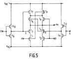
- FIG. 5 shows the circuit diagram of the circuit which has, by way of example, two input terminals.
- the input signals are indicated by a and b
- the inverse signals are indicated by a ⁇ and b ⁇ , respectively.
- the circuit comprises four n -channel transistors Tl, T2, T3 and T4 and four p -channel transistors T5, T6, T7 and T8.
- the supply line (for example 5 V) is designated by Vdd, while Vss indicates the earth line.
- the transistors T1, T3, T5 and T7 constitute a first series branch between Vdd and Vss and the transistors T2, T4, T6 and T8 constitute a second series branch.
- the drain zones of T7 and T8 are interconnected.
- the drain zones of T5 and T6 are connected to each other and also to the output terminal Vo.
- the drain zones of T3 and T4 are also connected to Vo.
- the input signal a is applied to the gates of T1 and T8, while the input signal b is applied to the gates of T2 and T6.
- the inverse signals a ⁇ and b ⁇ are applied to the gates of T4 and T5 and to the gates of T3 and T7, respectively.
- the inverter for the signal b comprises an n -channel transistor T9 and a p -channel transistor T10.
- the source zones of T9 and T10 are connected to Vss and to Vdd, respectively.
- the drain zones of T9 and T10 are connected to the gate electrodes of T3 and T7.
- the input signal b is supplied to the gate electrodes of T9 and T10.
- the output signal b ⁇ is derived at the drain zones of T9 and T10 and is supplied to the gate electrodes of T3 and T7.
- the input signal a is inverted by means of the inverter T11, T12, T11 being an n -channel transistor and T12 being a p -channel transistor.
- the dimensions of the transistors T9 and T12 can be very small because the inverters are practically not loaded.
- the transistors T1-T8 on the contrary are chosen to be considerably larger.
- Fig. 6 shows a possible embodiment of the circuit according to Fig. 5, which embodiment is very compact due to the combination of one row of wide transistors and two rows of narrow transistors.
- the wirings are simply indicated by a broken line. Where connections cross each other, they can be formed in two different wiring layers electrically insulated from each other. In the embodiment described here, two wiring layers are sufficient besides the aforementioned polycrystalline silicon layer, in which the gate electrodes are formed. Contacts between the wiring layers and zones or gate electrodes are indicated by a dot.
- the earth line Vss is connected to the gates 7,1 and 7,6 of the system of n -channel transistors. Under these gates, no conducting channels can be formed, as a result of which an effective electrical insulation between the circuit and adjacent circuits is obtained.
- the supply line Vdd is connected to the gates 10,1 and 10,6.
- the gate 7,2 is connected to the gate 10,2, while the gate 7,3 is connected to the gate 10,3 and gates 7,4 and 7,5 are connected to the gates 10,4 and 10,5 respectively.
- the input signals a and b are supplied, for example, via signal lines (not shown in the drawing) to the gates 7,3/10,3 and 7,4/10,4, respectively.
- the potential Vss is applied to the n -type zones 20 and 21 of the narrow rows of n -channel transistors and to the n -zone 22 of the wide row of n -channel transistors.
- the potential Vdd is applied to the p -type zones 23, 24 of the narrow rows of p -channel transistors and to the p -type zone 25 of the wide central row.
- the n -channel transistor T11 is constituted by the gate 7,3, the narrow n -type zone 20 constituting the source zone and the narrow n -type zone 26 constituting the drain zone.
- the zone 26 is connected via the gates 7,5 and 10,5 to the p -type zone 27 in the row 9.
- This zone constitutes the drain of the p -channel transistor T12, whose gate is constituted by the electrode 10,3 and whose source is constituted by the p -type zone 23.
- the n -channel transistor T9 is located in the narrow row 6 and comprises the gate 7,4 and the n -type zones 21 and 28 constituting the source and the drain, respectively.
- the zone 28 supplying the inverted signal b ⁇ is connected to the gate electrodes 7,2 and 10,2 and to the p -type zone 29 in the narrow row 8.
- the zone 29 is the drain zone of the p -channel transistor T10, whose gate is constituted by the gate 10,4 and whose source is constituted by the p -type zone 24.
- the n -channel transistor T1 comprises the n -type zone 22 as source, the n-type zone 30 as drain and the gate electrode 7,3, to which the signal a is applied.
- the zone 30 at the same time constitutes the source of the n -channel transistor T3 having the gate 7,2 for the signal b and the n -type zone 31 as drain.
- the n -channel transistor T2 comprises the source zone 22, the gate 7,4 and the drain zone 32.
- the latter zone constitutes at the same time the source of the n -channel transistor T4, whose gate electrode comprises the gate 7,5 and whose drain is constituted by the n -type zone 33.
- the drain zones 31 and 33 are interconnected by means of the connection 34, which may be connected to the output terminal Vo for deriving the output signal.
- the p -channel transistor T7 comprises as source the (wide) p -type zone 25, the gate electrode 10,2 and as drain zone the p -type zone 35.
- the p -channel transistor T8 also comprises as source the zone 25, the gate electrode 10,3 and as drain the p -type zone 36.
- the drain zones 35 and 36 of the parallel-connected transistors T7 and T8 are connected to each other and to the p -type zone 37, which constitutes the source zone of the p -channel transistor T5.
- the gate electrode of T5 is constituted by the gate 10,5 (signal a ⁇ ) and the drain zone is constituted by the p -type zone 38.
- This zone constitutes at the same time the drain zone of the p -channel transistor T6, which has the gate electrode 10,4 and whose source zone is constituted by the p -type zone 36.
- the zone 38 is connected to the connection 34, from which an output signal Vo can be derived.
- Both in the n -channel region and in the p -channel region more than the three said rows may be arranged, as the case may be having the width of the narrow rows.
- Exclusive NOR circuit also other logic gates and/or memory circuits in the gate array described here may be mentioned.
Landscapes
- Design And Manufacture Of Integrated Circuits (AREA)
- Metal-Oxide And Bipolar Metal-Oxide Semiconductor Integrated Circuits (AREA)
- Tone Control, Compression And Expansion, Limiting Amplitude (AREA)
- Logic Circuits (AREA)
Claims (1)
- Integrierte CMOS-Schaltung vom Gate-Array-Typ mit einem Halbleiterkörper (1), der an einer Oberfläche versehen ist mit:einer ersten Reihe (5) und einer benachbarten parallelen zweiten Reihe (6) aus n-Kanal-MOS-Transistoren mit gemeinsamen Gate-Elektroden (7) in Form von Leiterbahnen, die quer zur Reihenrichtung über beide Reihen verlaufen, wobei die n-Kanal-MOS-Transistoren der genannten ersten und zweiten Reihe gleiche Kanalbreiten haben;einer ersten Reihe (8) und einer benachbarten parallelen zweiten Reihe (9) aus p-Kanal-MOS-Transistoren mit gemeinsamen Gate-Elektroden (10) in Form von Leiterbahnen, die quer zur Reihenrichtung über beide Reihen verlaufen, wobei die p-Kanal-MOS-Transistoren der genannten ersten und zweiten Reihe gleiche Kanalbreiten haben;dadurch gekennzeichnet, daß neben der ersten und zweiten Reihe aus n-Kanal-MOS-Transistoren eine dritte Reihe (11) aus n-Kanal-MOS-Transistoren liegt, die parallel zur ersten und zweiten Reihe verläuft, wobei die Gate-Elektroden (7) der ersten und der zweiten Reihe aus n-Kanal-MOS-Transistoren auch Gate-Elektroden der genannten dritten Reihe aus n-Kanal-MOS-Transistoren bilden, und daß neben der ersten und zweiten Reihe aus p-Kanal-MOS-Transistoren eine dritte Reihe (12) aus p-Kanal-MOS-Transistoren liegt, die parallel zur ersten und zweiten Reihe verläuft, wobei die Gate-Elektroden (10) der ersten und der zweiten Reihe aus p-Kanal-MOS-Transistoren auch Gate-Elektroden der genannten dritten Reihe aus p-Kanal-MOS-Transistoren bilden, worin die Transistoren der dritten Reihe aus n-Kanal-MOS-Transistoren eine Kanalbreite haben, die zumindest viermal so groß wie die Kanalbreite der Transistoren der ersten und der zweiten Reihe aus n-Kanal-MOS-Transistoren ist und die Transistoren der dritten Reihe aus p-Kanal-MOS-Transistoren eine Kanalbreite haben, die zumindest viermal so groß wie die Kanalbreite der Transistoren der ersten und der zweiten Reihe aus p-Kanal-MOS-Transistoren ist, wobei die dritte Reihe aus n-Kanal-MOS-Transistoren zwischen der ersten und der zweiten Reihe aus n-Kanal-MOS-Transistoren liegt und die dritte Reihe aus p-Kanal-MOS-Transistoren zwischen der ersten und der zweiten Reihe aus p-Kanal-MOS-Transistoren liegt.
Applications Claiming Priority (2)
| Application Number | Priority Date | Filing Date | Title |
|---|---|---|---|
| NL8902629 | 1989-10-24 | ||
| NL8902629A NL8902629A (nl) | 1989-10-24 | 1989-10-24 | Geintegreerde cmos-schakeling. |
Publications (2)
| Publication Number | Publication Date |
|---|---|
| EP0425032A1 EP0425032A1 (de) | 1991-05-02 |
| EP0425032B1 true EP0425032B1 (de) | 1997-01-08 |
Family
ID=19855506
Family Applications (1)
| Application Number | Title | Priority Date | Filing Date |
|---|---|---|---|
| EP90202798A Expired - Lifetime EP0425032B1 (de) | 1989-10-24 | 1990-10-19 | Integrierte CMOS-Schaltung |
Country Status (8)
| Country | Link |
|---|---|
| EP (1) | EP0425032B1 (de) |
| JP (1) | JP3060235B2 (de) |
| KR (1) | KR0185976B1 (de) |
| AT (1) | ATE147543T1 (de) |
| DE (1) | DE69029642T2 (de) |
| NL (1) | NL8902629A (de) |
| RU (1) | RU2025829C1 (de) |
| UA (1) | UA27693C2 (de) |
Families Citing this family (1)
| Publication number | Priority date | Publication date | Assignee | Title |
|---|---|---|---|---|
| US5391943A (en) * | 1994-01-10 | 1995-02-21 | Mahant-Shetti; Shivaling S. | Gate array cell with predefined connection patterns |
Family Cites Families (2)
| Publication number | Priority date | Publication date | Assignee | Title |
|---|---|---|---|---|
| JPS60130140A (ja) * | 1983-12-17 | 1985-07-11 | Toshiba Corp | 半導体集積回路装置 |
| JPH0695570B2 (ja) * | 1985-02-07 | 1994-11-24 | 三菱電機株式会社 | 半導体集積回路装置 |
-
1989
- 1989-10-24 NL NL8902629A patent/NL8902629A/nl not_active Application Discontinuation
-
1990
- 1990-10-19 DE DE69029642T patent/DE69029642T2/de not_active Expired - Fee Related
- 1990-10-19 EP EP90202798A patent/EP0425032B1/de not_active Expired - Lifetime
- 1990-10-19 AT AT90202798T patent/ATE147543T1/de not_active IP Right Cessation
- 1990-10-22 UA UA4831588A patent/UA27693C2/uk unknown
- 1990-10-22 KR KR1019900016859A patent/KR0185976B1/ko not_active Expired - Fee Related
- 1990-10-22 JP JP2284126A patent/JP3060235B2/ja not_active Expired - Fee Related
- 1990-10-22 RU SU4831588/25A patent/RU2025829C1/ru not_active IP Right Cessation
Also Published As
| Publication number | Publication date |
|---|---|
| KR910008818A (ko) | 1991-05-31 |
| NL8902629A (nl) | 1991-05-16 |
| UA27693C2 (uk) | 2000-10-16 |
| KR0185976B1 (en) | 1999-04-15 |
| JP3060235B2 (ja) | 2000-07-10 |
| DE69029642D1 (de) | 1997-02-20 |
| JPH03152970A (ja) | 1991-06-28 |
| ATE147543T1 (de) | 1997-01-15 |
| DE69029642T2 (de) | 1997-07-10 |
| EP0425032A1 (de) | 1991-05-02 |
| RU2025829C1 (ru) | 1994-12-30 |
Similar Documents
| Publication | Publication Date | Title |
|---|---|---|
| US6084255A (en) | Gate array semiconductor device | |
| US6166415A (en) | Semiconductor device with improved noise resistivity | |
| EP0098163B1 (de) | Gattermatrixchip | |
| KR940002772B1 (ko) | 반도체 집적회로 장치 및 그 제조방법 | |
| US6642588B1 (en) | Latch-up prevention for memory cells | |
| KR890003147B1 (ko) | 게이트 에레이 | |
| EP0080361B1 (de) | Komplementaire Metalloxidhalbleiter enthaltende integrierte Schaltungsvorrichtung in Mutterscheibentechnik | |
| EP0348998B1 (de) | Integrierte Halbleiterschaltung, bestehend aus einer Differenztransistorschaltung mit einem Paar von FETs | |
| EP0177336B1 (de) | Integrierte Gate-Matrixstruktur | |
| US6740937B1 (en) | Basic cells configurable into different types of semiconductor integrated circuits | |
| US5714796A (en) | Integrated circuit device fabricated on semiconductor substrate blocking power supply lines from noise | |
| US5083178A (en) | Semiconductor cmos gate array | |
| US5206184A (en) | Method of making single layer personalization | |
| US5229667A (en) | Delay unit implemented by inverting circuits associated with capacitive load for increasing delay | |
| EP0137257B1 (de) | Logische Familie mit Widerstandstor-Feldeffekttransistoren | |
| US5250823A (en) | Integrated CMOS gate-array circuit | |
| US4034243A (en) | Logic array structure for depletion mode-FET load circuit technologies | |
| US4853562A (en) | Programmable logic array using single transistor to generate true or complement signal | |
| EP0092176B1 (de) | Basiszelle für integrierte Verknüpfungsschaltungsfelder | |
| EP0425032A1 (de) | Integrierte CMOS-Schaltung | |
| JP2840150B2 (ja) | 半導体集積回路及びその層間接続方法 | |
| EP0318869B1 (de) | Substratpotentialdetektionsschaltung | |
| US4143390A (en) | Semiconductor device and a logical circuit formed of the same | |
| JP3076248B2 (ja) | 半導体記憶回路 | |
| EP0281590B1 (de) | Integrierte schaltung in hauptscheibentechnik |
Legal Events
| Date | Code | Title | Description |
|---|---|---|---|
| PUAI | Public reference made under article 153(3) epc to a published international application that has entered the european phase |
Free format text: ORIGINAL CODE: 0009012 |
|
| AK | Designated contracting states |
Kind code of ref document: A1 Designated state(s): AT CH DE FR GB IT LI NL |
|
| 17P | Request for examination filed |
Effective date: 19911028 |
|
| 17Q | First examination report despatched |
Effective date: 19940421 |
|
| GRAG | Despatch of communication of intention to grant |
Free format text: ORIGINAL CODE: EPIDOS AGRA |
|
| GRAH | Despatch of communication of intention to grant a patent |
Free format text: ORIGINAL CODE: EPIDOS IGRA |
|
| GRAH | Despatch of communication of intention to grant a patent |
Free format text: ORIGINAL CODE: EPIDOS IGRA |
|
| GRAA | (expected) grant |
Free format text: ORIGINAL CODE: 0009210 |
|
| AK | Designated contracting states |
Kind code of ref document: B1 Designated state(s): AT CH DE FR GB IT LI NL |
|
| REF | Corresponds to: |
Ref document number: 147543 Country of ref document: AT Date of ref document: 19970115 Kind code of ref document: T |
|
| REG | Reference to a national code |
Ref country code: CH Ref legal event code: EP |
|
| REF | Corresponds to: |
Ref document number: 69029642 Country of ref document: DE Date of ref document: 19970220 |
|
| ITF | It: translation for a ep patent filed | ||
| ET | Fr: translation filed | ||
| PLBE | No opposition filed within time limit |
Free format text: ORIGINAL CODE: 0009261 |
|
| STAA | Information on the status of an ep patent application or granted ep patent |
Free format text: STATUS: NO OPPOSITION FILED WITHIN TIME LIMIT |
|
| 26N | No opposition filed | ||
| REG | Reference to a national code |
Ref country code: CH Ref legal event code: PFA Free format text: PHILIPS ELECTRONICS N.V. TRANSFER- KONINKLIJKE PHILIPS ELECTRONICS N.V. |
|
| NLT1 | Nl: modifications of names registered in virtue of documents presented to the patent office pursuant to art. 16 a, paragraph 1 |
Owner name: KONINKLIJKE PHILIPS ELECTRONICS N.V. |
|
| REG | Reference to a national code |
Ref country code: FR Ref legal event code: CD |
|
| REG | Reference to a national code |
Ref country code: GB Ref legal event code: IF02 |
|
| PGFP | Annual fee paid to national office [announced via postgrant information from national office to epo] |
Ref country code: CH Payment date: 20020108 Year of fee payment: 12 |
|
| REG | Reference to a national code |
Ref country code: GB Ref legal event code: 746 Effective date: 20020911 |
|
| PGFP | Annual fee paid to national office [announced via postgrant information from national office to epo] |
Ref country code: NL Payment date: 20021028 Year of fee payment: 13 Ref country code: FR Payment date: 20021028 Year of fee payment: 13 Ref country code: AT Payment date: 20021028 Year of fee payment: 13 |
|
| PGFP | Annual fee paid to national office [announced via postgrant information from national office to epo] |
Ref country code: GB Payment date: 20021030 Year of fee payment: 13 |
|
| PG25 | Lapsed in a contracting state [announced via postgrant information from national office to epo] |
Ref country code: LI Free format text: LAPSE BECAUSE OF THE APPLICANT RENOUNCES Effective date: 20021031 Ref country code: CH Free format text: LAPSE BECAUSE OF THE APPLICANT RENOUNCES Effective date: 20021031 |
|
| REG | Reference to a national code |
Ref country code: FR Ref legal event code: D6 |
|
| REG | Reference to a national code |
Ref country code: CH Ref legal event code: PL |
|
| PGFP | Annual fee paid to national office [announced via postgrant information from national office to epo] |
Ref country code: DE Payment date: 20030201 Year of fee payment: 13 |
|
| PG25 | Lapsed in a contracting state [announced via postgrant information from national office to epo] |
Ref country code: GB Free format text: LAPSE BECAUSE OF NON-PAYMENT OF DUE FEES Effective date: 20031019 Ref country code: AT Free format text: LAPSE BECAUSE OF NON-PAYMENT OF DUE FEES Effective date: 20031019 |
|
| PG25 | Lapsed in a contracting state [announced via postgrant information from national office to epo] |
Ref country code: NL Free format text: LAPSE BECAUSE OF NON-PAYMENT OF DUE FEES Effective date: 20040501 Ref country code: DE Free format text: LAPSE BECAUSE OF NON-PAYMENT OF DUE FEES Effective date: 20040501 |
|
| GBPC | Gb: european patent ceased through non-payment of renewal fee |
Effective date: 20031019 |
|
| PG25 | Lapsed in a contracting state [announced via postgrant information from national office to epo] |
Ref country code: FR Free format text: LAPSE BECAUSE OF NON-PAYMENT OF DUE FEES Effective date: 20040630 |
|
| NLV4 | Nl: lapsed or anulled due to non-payment of the annual fee |
Effective date: 20040501 |
|
| REG | Reference to a national code |
Ref country code: FR Ref legal event code: ST |
|
| PG25 | Lapsed in a contracting state [announced via postgrant information from national office to epo] |
Ref country code: IT Free format text: LAPSE BECAUSE OF NON-PAYMENT OF DUE FEES;WARNING: LAPSES OF ITALIAN PATENTS WITH EFFECTIVE DATE BEFORE 2007 MAY HAVE OCCURRED AT ANY TIME BEFORE 2007. THE CORRECT EFFECTIVE DATE MAY BE DIFFERENT FROM THE ONE RECORDED. Effective date: 20051019 |