EP0425186A2 - Z-Puffersteuerung - Google Patents
Z-Puffersteuerung Download PDFInfo
- Publication number
- EP0425186A2 EP0425186A2 EP90311389A EP90311389A EP0425186A2 EP 0425186 A2 EP0425186 A2 EP 0425186A2 EP 90311389 A EP90311389 A EP 90311389A EP 90311389 A EP90311389 A EP 90311389A EP 0425186 A2 EP0425186 A2 EP 0425186A2
- Authority
- EP
- European Patent Office
- Prior art keywords
- pixel
- pixels
- depth value
- memory
- buffer
- Prior art date
- Legal status (The legal status is an assumption and is not a legal conclusion. Google has not performed a legal analysis and makes no representation as to the accuracy of the status listed.)
- Withdrawn
Links
Images


Classifications
-
- G—PHYSICS
- G06—COMPUTING OR CALCULATING; COUNTING
- G06T—IMAGE DATA PROCESSING OR GENERATION, IN GENERAL
- G06T15/00—Three-dimensional [3D] image rendering
- G06T15/10—Geometric effects
- G06T15/40—Hidden part removal
- G06T15/405—Hidden part removal using Z-buffer
Definitions
- the present invention relates to methods and apparatus for displaying graphics objects.
- Computer graphics systems are frequently used to model three dimensional objects and then display them on a two dimensional output device such as a cathode ray tube. Displaying three dimensional objects on a two dimensional display device requires the system to recognize and eliminate hidden surfaces and lines to obtain the desired three dimensional affect.
- One method for eliminating hidden surfaces of the image involves the use of a depth buffer or Z-buffer.
- the Z-buffer is a large array of memory with an entry for each picture element, or pixel, on the display device.
- the Z axis in a graphics system reflects the distance from a specified observer's viewpoint. Thus, a larger Z value represents a greater distance from the viewpoint.
- a comparison of Z values of points on the generated objects determines which object is closest to the viewpoint and therefore should appear on the two dimensional display.
- Z-buffer systems as each pixel is generated its Z coordinate (ZNEW) is compared with the Z coordinate previously stored in the Z-buffer (ZOLD). If ZOLD does not exist, then ZNEW is compared to the Z coordinate of the background. If ZNEW is less than ZOLD (indicating that this pixel is closer to the viewpoint than the previous viewpoint), then the pixel is written to the display device and the Z-buffer memory is updated to contain ZNEW.
- DRAM dynamic random access memory
- SRAM static random access memory
- the typical computer graphics processor is capable of generating pixel data at high speed, typically 100 ns per pixel, and a display device is typically capable for receiving pixel data at equally high speeds. Therefore the slow RMW cycle time of the DRAM is a limiting factor in the ability to speed the display generation process.
- a graphics display system for processing graphic orders and displaying objects on a display device, wherein said processing removes hidden surfaces
- said system comprising: graphic processor means for processing graphic orders and generating a plurality of picture elements each having a depth value, said processor means operating at a pixel generation rate; memory means for storing a depth value for each picture element of said display device, said memory means having a pixel access rate; accumulator means for accumulating a set of picture elements from said plurality of generated elements; memory controller means for accessing a plurality of depth values in said memory means corresponding to said set of picture elements; comparing means for comparing, in parallel, each of said picture elements with an associated depth buffer element; and serialization means for generating picture elements for display, said serialization means being responsive to said comparing means and generating a picture element only when said depth value of said generated picture element is nearer a set viewpoint that said depth value in said memory means.
- the present invention enables Z-buffer comparisons to be performed at the rate of graphics system pixel generation using DRAMs whose pixel read-modify-write cycle time is greater than the pixel generation cycle time.
- a method for removing hidden surfaces in a graphics display system having a graphic processor for generating a plurality of pixels representing a graphics object, each pixel having a depth value representing a distance from a viewpoint, and a depth buffer having a stored depth value representing a previous pixel distance to said viewpoint for each pixel of a graphic display device, and wherein said pixels are generated at a first rate
- the method comprising the steps of: defining a processing cell containing a fixed number of pixel elements; accumulating generated pixels into said cell; accessing said memory to return depth values for a plurality of plxels corresponding to said accumulated pixels; comparing, in parallel, said generated depth value to said depth value in said memory; and generating serial pixels for each pixel for which the generated depth value is closer to said viewpoint than said stored depth value.
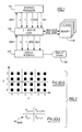
- the graphics processor 100 generates the X, Y, and Z coordinates for each pixel of an object to be rendered. Three axis coordinates and a color, usually specified by red, green, and blue components (RGB) are generated for each pixel as required to describe the object.
- the graphics processor may start at any X, Y, Z coordinate location and generate a sequence of adjacent pixels proceeding in the horizontal, vertical or diagonal directions. In the preferred embodiment, the processors generates an "END" signal when no more pixel data is to follow.
- a signal "ZRDY" is generated by the Z-buffer controller 102 to indicate the Z-buffer is ready to accept pixel data.
- the display interface 104 accepts pixel data in the form of two-dimensional coordinates (X, Y) and color (R, G, B).
- a signal "WPIX” indicates whether or not the pixel should be written on the display device. Only those pixels that are visible have an active WPIX value.
- the signal "DRDY” indicates the display interface is ready to receive pixel data.
- the display interface operates to generate the signals necessary to display the graphic image on display device 106. Although a CRT or monitor device is shown in the preferred embodiment, the techniques employed herein work equally well for any two dimensional display device such as a plotter, printer, or other monitor type.
- Z-buffer control logic 102 controls the evaluation of each Z coordinate to eliminate surfaces or lines which are hidden behind other surfaces.
- the Z-buffer is provided with Z-buffer memory 108 in which each pixel on the display device has a corresponding entry.
- the buffer memory 108 in the preferred embodiment, consists of multiple dynamic random access memory (DRAM) modules that can be accessed simultaneously in a single memory access cycle.
- DRAM dynamic random access memory
- the Z-buffer controller accumulates the pixel data from the graphics processor for adjacent pixels and then performs Z-buffer comparison in parallel for the collected pixels. All pixels whose ZNEW is less than ZOLD are updated in parallel and the corresponding X, Y, and color data sent to the display interface. Otherwise, that pixel data is discarded. By accumulating pixels with related Z-buffer memory addresses and processing them in parallel, the time penalty paid for accessing, comparing, and updating the Z-buffer memory is distributed over multiple pals. Once the comparison has been made, the pixel data is reserialized for display by the display interface.
- the number of DRAM modules or independent address paths required to implement the present invention is determined by the relative speeds of DRAM access and pixel generation from the graphics processor.
- compare and update time 200 nanoseconds and a pixel generation rate of .01 pixels per nanosecond (100 nanoseconds per pixel) the number of pixels to be compared must be at least two.
- the invention relates to simultaneously processing an m X n cell of pixels.
- four pixels can be simultaneously compared.
- the cells are 2x2, spanning two pixels horizontally and two pixels vertically. This grouping of four pixels is selected because a particular line generation may result in two horizontal, two vertical, or two diagonal pixels being generated for testing against the 2-buffer.
- the system has a high probability of having two or more pixels to access at each cycle.
- the pixels are addressed relative to a base pixel, XY base .
- the controller is arranged to perform a comparison whenever the end of pixel data is reached or line generation causes a crossing of a cell boundary.
- simultaneous Z-buffer access for adjacent pixels is provided by having four DRAM modules addressable by a single address.
- Various other DRAM arrangements are possible as long as multiple pixel addresses can be accessed during a single processing cycle. By specifying a single address for accessing the four DRAMs the number of address lines required can be reduced.
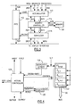
- Z-buffer control logic 102 is shown in greater detail in Fig. 3.
- Accumulator 110 performs the function of collecting pixels generated by the graphics processor into cells. The accumulator tags each pixel data point with the order in which it arrived at the accumulator. The order is used to reserialize the pixels after the Z-buffer comparison. Finally, the accumulator detects the crossing of a cell boundary or the end of pixel data. Because the RGB components are unnecessary to the Z-buffer comparison, the controller according to the preferred embodiment of the present invention loads the RGB values into a first-in first-out (FIFO) queue 112 for later reference. These values could be carried with the pixels passed by the accumulator if desired.
- FIFO first-in first-out
- the accumulator passes the accumulated cell of pixels to memory controller 114.
- the memory controller 114 accesses memory 108, performs the comparison and, for all those pixels for which ZNEW ⁇ ZOLD, writes ZNEW to memory and tags the pixels as being visible. All other pixels are tagged as invisible (i.e. those pixels with ZNEW ⁇ ZOLD, those beyond a previously written pixel).
- Controller 114 passes the results from controller 114 to serializer 116 that generates single pixels and transmits each pixel value to the display interface. If the pixel has been tagged as visible, then the WPIX value is active and the FIFO queue is unloaded into the display interface. Otherwise WPIX is inactive and the FIFO is unloaded and discarded.
- each pixel in the cell is tag with its order of generation because the Z coordinate stored for comparison is arranged only by position in the cell.
- the cell ordering is not guaranteed to be the same as the the pixels were generated by the graphics processor.
- the order tag is used by the control logic to reserialize pixels in the order generated.
- a block diagram of accumulator 110 is presented in Fig. 4.
- Counter 120 is initially reset to an initial value.
- a valid pixel is received from the graphics processor, its X,Y components are examined and the Z coordinate loaded into an appropriate p i,j register and the coordinate of the lower left corner of the cell loaded into the XY base .
- p the Z values, p, are compared to the respective modules, i.e.p X,Y to the first module, p X+1Y to the second and so on.
- each module is independently addressable, the address for each pixel in the cell would need to be retained.
- Each of the registers 122 is the format as shown in Fig. 5a.
- the first field, Z is the Z coordinate of the pixel being stored.
- Field L indicates that this is the last pixel for the cell to be loaded.
- V indicates the register is valid, and C is the value of counter 120 when this pixel is loaded.
- Counter 120 is incremented after each pixel. By storing the counter in each pixel register, the order in which the pixels were generated can be recovered by serializer 116.
- the END signal is transmitted by graphics processor or boundary detect 126 detects the crossing of a cell boundary, the field L is set in the current p i,j and the counter 120 reset to its initial value.
- the set of registers 122 are then passed to the memory controller 114 along bus 130. Controller 128 controls the process of loading the registers 122, passing RGB data to the FIFO queue, and communicating with the graphics processor and memory controller.
- Memory controller 114 is shown in greater detail in Fig. 6.
- the value stored in registers 122 by the accumulator are passed via bus 130 to registers 132 in the memory controller.
- the registers in the controller are arranged in an identical order with an XY base and values g X,Y for each of the pixels.
- the register address XY base 136 is used to access DRAM modules 108.
- Data from DRAM modules 108 is passed along data lines to comparators 138, 140, 142, 144 which compare the ZOLD from memory 108 to the ZNEW values in the registers 132.
- Each register q i,j has a format as shown in Fig. 5(b).
- the values Z, V, L, and C are equivalent to those of p i,j .
- q i,j has the value W which is set according to the output of the respective comparator. For a particular pixel, if ZNEW ⁇ ZOLD and field V is true, then ZNEW is written to memory and field W is set true.
- memory controller logic transfers data from q i,j to the serializer along bus 146. Only the fields L, C, and W are transferred. The Z coordinate itself is no longer required.
- Serializer 116 is shown in greater detail in Fig. 7.
- the data from memory controller 114 is passed along bus 146 into registers 148.
- the format of the registers r i,j is shown in Fig. 5(c).
- the serializer 116 must serializer the r i,j into the order in which they were generated by the graphics processor and write them to the display interface if field W is true.
- Counter 150 is first set to an initialize value.
- Registers 148 act as an associative memory in the preferred embodiment with the output of counter 150 as the input register.
- the matching r i,j value causes L and W to be passed to the serializer controller 152.
- Combinatorial logic 154 computes an X and Y address for each step of the counter. If field W in r i,j is active, then X, Y, R, G, and B are placed on the display interface with WPIX having a true value. Otherwise, WPIX is inactive and the FIFO is simply unloaded. In either case, the counter is incremented and the process repeated. If field L indicating the last pixel in the current cell, is true, then the counter is reset to its initial value.
- accumulator 110 can be loading the 3D pixels from a given cell n while memory controller 114 is comparing the Z coordinates from cell n-1 while serializer 116 is unloading two dimensional pixels from n-2.
- the high speed operation occurs because pixels are generated sequentially and written to the display sequentially but the access, compare, and update of the Z-buffer is performed in parallel.
Landscapes
- Physics & Mathematics (AREA)
- Engineering & Computer Science (AREA)
- Geometry (AREA)
- Computer Graphics (AREA)
- General Physics & Mathematics (AREA)
- Theoretical Computer Science (AREA)
- Image Generation (AREA)
- Controls And Circuits For Display Device (AREA)
Applications Claiming Priority (2)
| Application Number | Priority Date | Filing Date | Title |
|---|---|---|---|
| US425778 | 1989-10-23 | ||
| US07/425,778 US5043921A (en) | 1989-10-23 | 1989-10-23 | High speed Z-buffer control |
Publications (2)
| Publication Number | Publication Date |
|---|---|
| EP0425186A2 true EP0425186A2 (de) | 1991-05-02 |
| EP0425186A3 EP0425186A3 (en) | 1993-02-03 |
Family
ID=23687996
Family Applications (1)
| Application Number | Title | Priority Date | Filing Date |
|---|---|---|---|
| EP19900311389 Withdrawn EP0425186A3 (en) | 1989-10-23 | 1990-10-17 | Z-buffer control |
Country Status (3)
| Country | Link |
|---|---|
| US (1) | US5043921A (de) |
| EP (1) | EP0425186A3 (de) |
| JP (1) | JPH07104960B2 (de) |
Cited By (1)
| Publication number | Priority date | Publication date | Assignee | Title |
|---|---|---|---|---|
| EP0757833A1 (de) * | 1994-04-29 | 1997-02-12 | Cirrus Logic | Variable pixeltiefe und format für video-fenster |
Families Citing this family (21)
| Publication number | Priority date | Publication date | Assignee | Title |
|---|---|---|---|---|
| US5265198A (en) * | 1989-10-23 | 1993-11-23 | International Business Machines Corporation | Method and processor for drawing `polygon with edge`-type primitives in a computer graphics display system |
| JPH04335422A (ja) * | 1991-05-10 | 1992-11-24 | Ricoh Co Ltd | ソーティング装置 |
| US5265199A (en) * | 1991-05-22 | 1993-11-23 | Silicon Graphics, Inc. | Method and apparatus for accomplishing Z-buffering by prediction |
| US5359704A (en) * | 1991-10-30 | 1994-10-25 | International Business Machines Corporation | Method for selecting silhouette and visible edges in wire frame images in a computer graphics display system |
| US5319388A (en) * | 1992-06-22 | 1994-06-07 | Vlsi Technology, Inc. | VGA controlled having frame buffer memory arbitration and method therefor |
| US5621866A (en) * | 1992-07-24 | 1997-04-15 | Fujitsu Limited | Image processing apparatus having improved frame buffer with Z buffer and SAM port |
| US5321809A (en) * | 1992-09-11 | 1994-06-14 | International Business Machines Corporation | Categorized pixel variable buffering and processing for a graphics system |
| TW241196B (de) * | 1993-01-15 | 1995-02-21 | Du Pont | |
| WO1994027240A1 (en) * | 1993-05-10 | 1994-11-24 | Apple Computer, Inc. | Computer graphics system having high performance multiple layer z-buffer |
| DE19508774A1 (de) * | 1995-03-03 | 1996-09-05 | Univ Tuebingen | Verfahren und Vorrichtung zur Überabtastung von Bildelementen |
| US5767856A (en) * | 1995-08-22 | 1998-06-16 | Rendition, Inc. | Pixel engine pipeline for a 3D graphics accelerator |
| US5933156A (en) * | 1997-12-03 | 1999-08-03 | Margolin; Jed | Z-Buffer for row addressable graphics memory with flash fill |
| US6747645B1 (en) * | 1998-03-13 | 2004-06-08 | Hewlett-Packard Development Company, L.P. | Graphics memory system that utilizes detached-Z buffering in conjunction with a batching architecture to reduce paging overhead |
| TW431069B (en) * | 2000-04-07 | 2001-04-21 | Via Tech Inc | High-speed data buffer |
| US8390619B1 (en) | 2003-12-22 | 2013-03-05 | Nvidia Corporation | Occlusion prediction graphics processing system and method |
| US8854364B1 (en) | 2003-12-22 | 2014-10-07 | Nvidia Corporation | Tight depth range occlusion prediction system and method |
| US7995056B1 (en) | 2003-12-22 | 2011-08-09 | Nvidia Corporation | Culling data selection system and method |
| US8269769B1 (en) * | 2003-12-22 | 2012-09-18 | Nvidia Corporation | Occlusion prediction compression system and method |
| US8878849B2 (en) * | 2007-12-14 | 2014-11-04 | Nvidia Corporation | Horizon split ambient occlusion |
| US10008029B2 (en) | 2013-05-31 | 2018-06-26 | Nvidia Corporation | Updating depth related graphics data |
| US9418400B2 (en) | 2013-06-18 | 2016-08-16 | Nvidia Corporation | Method and system for rendering simulated depth-of-field visual effect |
Family Cites Families (7)
| Publication number | Priority date | Publication date | Assignee | Title |
|---|---|---|---|---|
| US4658247A (en) * | 1984-07-30 | 1987-04-14 | Cornell Research Foundation, Inc. | Pipelined, line buffered real-time color graphics display system |
| US4679041A (en) * | 1985-06-13 | 1987-07-07 | Sun Microsystems, Inc. | High speed Z-buffer with dynamic random access memory |
| FR2586838B1 (fr) * | 1985-08-30 | 1989-07-28 | Labo Electronique Physique | Processeur d'elimination de faces cachees pour la synthese d'images a trois dimensions |
| JPS63271673A (ja) * | 1987-04-30 | 1988-11-09 | Toshiba Corp | 三次元表示装置 |
| JPS63307591A (ja) * | 1987-06-09 | 1988-12-15 | Agency Of Ind Science & Technol | 高機能zバッファメモリ |
| US4945500A (en) * | 1987-11-04 | 1990-07-31 | Schlumberger Technologies, Inc. | Triangle processor for 3-D graphics display system |
| US4951232A (en) * | 1988-09-12 | 1990-08-21 | Silicon Graphics, Inc. | Method for updating pipelined, single port Z-buffer by segments on a scan line |
-
1989
- 1989-10-23 US US07/425,778 patent/US5043921A/en not_active Expired - Lifetime
-
1990
- 1990-10-09 JP JP2269677A patent/JPH07104960B2/ja not_active Expired - Fee Related
- 1990-10-17 EP EP19900311389 patent/EP0425186A3/en not_active Withdrawn
Cited By (1)
| Publication number | Priority date | Publication date | Assignee | Title |
|---|---|---|---|---|
| EP0757833A1 (de) * | 1994-04-29 | 1997-02-12 | Cirrus Logic | Variable pixeltiefe und format für video-fenster |
Also Published As
| Publication number | Publication date |
|---|---|
| EP0425186A3 (en) | 1993-02-03 |
| US5043921A (en) | 1991-08-27 |
| JPH07104960B2 (ja) | 1995-11-13 |
| JPH03139780A (ja) | 1991-06-13 |
Similar Documents
| Publication | Publication Date | Title |
|---|---|---|
| US5043921A (en) | High speed Z-buffer control | |
| EP0433373B1 (de) | Wirksames verfahren zur aktualisierung eines zeitverschachtelt arbeitenden einzeltor-z-pufferspeichers | |
| EP0447225B1 (de) | Verfahren und Einrichtung zur Maximierung von Spaltenadressenkohärenz für den Zugriff von seriellen und Direktzugriffstoren in einem graphischen System mit einem Rasterpufferspeicher | |
| US5606650A (en) | Method and apparatus for storage and retrieval of a texture map in a graphics display system | |
| US4679041A (en) | High speed Z-buffer with dynamic random access memory | |
| US4594673A (en) | Hidden surface processor | |
| US5430841A (en) | Context management in a graphics system | |
| EP0279228B1 (de) | Bildspeicher für Raster-Video-Anzeige | |
| EP0704824B1 (de) | Organisation eines Z-Puffer-Etikettenspeichers | |
| GB2219470A (en) | Window crt display | |
| EP0613098A2 (de) | Bildverarbeitungsgerät und Verfahren um dieses zu Steuern | |
| US5321809A (en) | Categorized pixel variable buffering and processing for a graphics system | |
| US5621866A (en) | Image processing apparatus having improved frame buffer with Z buffer and SAM port | |
| US4912658A (en) | Method and apparatus for addressing video RAMS and refreshing a video monitor with a variable resolution | |
| US5050102A (en) | Apparatus for rapidly switching between output display frames using a shared frame gentification memory | |
| US5062142A (en) | Data processor producing a medial axis representation of an extended region | |
| KR0165464B1 (ko) | 그래픽을 위한 스팬렌더링방법 및 장치 | |
| EP0551251B1 (de) | Verfahren und vorrichtung zum auslöschen eines gebietes eines z-puffers | |
| EP0488441B1 (de) | Bildspeicheranordnung sowie Bildverarbeitungsanordnung mit der Bildspeicheranordnung | |
| EP0231780A2 (de) | Vektormusterverarbeitungsschaltung für eine Anzeigeeinheit mit einem Bitbildspeicher | |
| EP0410783B1 (de) | Verfahren und Einrichtung zur Beschleunigung von Bildfenstern in graphischen Systemen | |
| EI-Din et al. | Rapid video data capture and processing system for computer image measurement and analysis | |
| JPH0644385A (ja) | Zバッファ制御回路 | |
| GB2299919A (en) | Image processing apparatus | |
| JPH0584943B2 (de) |
Legal Events
| Date | Code | Title | Description |
|---|---|---|---|
| PUAI | Public reference made under article 153(3) epc to a published international application that has entered the european phase |
Free format text: ORIGINAL CODE: 0009012 |
|
| 17P | Request for examination filed |
Effective date: 19901213 |
|
| AK | Designated contracting states |
Kind code of ref document: A2 Designated state(s): DE FR GB IT |
|
| PUAL | Search report despatched |
Free format text: ORIGINAL CODE: 0009013 |
|
| AK | Designated contracting states |
Kind code of ref document: A3 Designated state(s): DE FR GB IT |
|
| 17Q | First examination report despatched |
Effective date: 19951218 |
|
| STAA | Information on the status of an ep patent application or granted ep patent |
Free format text: STATUS: THE APPLICATION IS DEEMED TO BE WITHDRAWN |
|
| 18D | Application deemed to be withdrawn |
Effective date: 19960626 |