EP0425262A2 - Absorbeurs - Google Patents
Absorbeurs Download PDFInfo
- Publication number
- EP0425262A2 EP0425262A2 EP90311642A EP90311642A EP0425262A2 EP 0425262 A2 EP0425262 A2 EP 0425262A2 EP 90311642 A EP90311642 A EP 90311642A EP 90311642 A EP90311642 A EP 90311642A EP 0425262 A2 EP0425262 A2 EP 0425262A2
- Authority
- EP
- European Patent Office
- Prior art keywords
- absorber
- absorber according
- conductive layer
- sheet
- electromagnetic energy
- Prior art date
- Legal status (The legal status is an assumption and is not a legal conclusion. Google has not performed a legal analysis and makes no representation as to the accuracy of the status listed.)
- Granted
Links
- 239000006096 absorbing agent Substances 0.000 title claims abstract description 45
- 239000004411 aluminium Substances 0.000 claims abstract description 8
- 229910052782 aluminium Inorganic materials 0.000 claims abstract description 8
- XAGFODPZIPBFFR-UHFFFAOYSA-N aluminium Chemical compound [Al] XAGFODPZIPBFFR-UHFFFAOYSA-N 0.000 claims abstract description 8
- 239000000463 material Substances 0.000 claims description 18
- 239000004744 fabric Substances 0.000 claims description 4
- 229920000728 polyester Polymers 0.000 claims description 4
- 229910001220 stainless steel Inorganic materials 0.000 claims description 3
- 239000010935 stainless steel Substances 0.000 claims description 3
- 239000002984 plastic foam Substances 0.000 claims description 2
- 238000000151 deposition Methods 0.000 claims 1
- 230000008021 deposition Effects 0.000 claims 1
- 238000004544 sputter deposition Methods 0.000 claims 1
- 239000004033 plastic Substances 0.000 abstract description 9
- 229920003023 plastic Polymers 0.000 abstract description 9
- 239000000758 substrate Substances 0.000 abstract description 6
- 229910052751 metal Inorganic materials 0.000 abstract description 5
- 239000002184 metal Substances 0.000 abstract description 5
- 239000011248 coating agent Substances 0.000 abstract description 4
- 238000000576 coating method Methods 0.000 abstract description 4
- 229920002972 Acrylic fiber Polymers 0.000 abstract description 3
- NIXOWILDQLNWCW-UHFFFAOYSA-N acrylic acid group Chemical group C(C=C)(=O)O NIXOWILDQLNWCW-UHFFFAOYSA-N 0.000 abstract description 3
- 239000002985 plastic film Substances 0.000 abstract description 3
- 238000010521 absorption reaction Methods 0.000 description 10
- 239000006260 foam Substances 0.000 description 10
- 230000003287 optical effect Effects 0.000 description 5
- 230000005540 biological transmission Effects 0.000 description 4
- 230000005670 electromagnetic radiation Effects 0.000 description 4
- 238000012986 modification Methods 0.000 description 3
- 230000004048 modification Effects 0.000 description 3
- 239000004020 conductor Substances 0.000 description 2
- 239000004800 polyvinyl chloride Substances 0.000 description 2
- 238000002310 reflectometry Methods 0.000 description 2
- 235000016936 Dendrocalamus strictus Nutrition 0.000 description 1
- 239000004698 Polyethylene Substances 0.000 description 1
- 230000000694 effects Effects 0.000 description 1
- 239000006261 foam material Substances 0.000 description 1
- 230000001771 impaired effect Effects 0.000 description 1
- 238000004519 manufacturing process Methods 0.000 description 1
- 238000005259 measurement Methods 0.000 description 1
- 238000000034 method Methods 0.000 description 1
- -1 polyethylene Polymers 0.000 description 1
- 229920000573 polyethylene Polymers 0.000 description 1
- 239000011148 porous material Substances 0.000 description 1
- 230000005855 radiation Effects 0.000 description 1
- 239000007787 solid Substances 0.000 description 1
- 239000012780 transparent material Substances 0.000 description 1
- 238000003466 welding Methods 0.000 description 1
Images

Classifications
-
- H—ELECTRICITY
- H01—ELECTRIC ELEMENTS
- H01Q—ANTENNAS, i.e. RADIO AERIALS
- H01Q17/00—Devices for absorbing waves radiated from an antenna; Combinations of such devices with active antenna elements or systems
-
- Y—GENERAL TAGGING OF NEW TECHNOLOGICAL DEVELOPMENTS; GENERAL TAGGING OF CROSS-SECTIONAL TECHNOLOGIES SPANNING OVER SEVERAL SECTIONS OF THE IPC; TECHNICAL SUBJECTS COVERED BY FORMER USPC CROSS-REFERENCE ART COLLECTIONS [XRACs] AND DIGESTS
- Y10—TECHNICAL SUBJECTS COVERED BY FORMER USPC
- Y10T—TECHNICAL SUBJECTS COVERED BY FORMER US CLASSIFICATION
- Y10T428/00—Stock material or miscellaneous articles
- Y10T428/26—Web or sheet containing structurally defined element or component, the element or component having a specified physical dimension
- Y10T428/268—Monolayer with structurally defined element
-
- Y—GENERAL TAGGING OF NEW TECHNOLOGICAL DEVELOPMENTS; GENERAL TAGGING OF CROSS-SECTIONAL TECHNOLOGIES SPANNING OVER SEVERAL SECTIONS OF THE IPC; TECHNICAL SUBJECTS COVERED BY FORMER USPC CROSS-REFERENCE ART COLLECTIONS [XRACs] AND DIGESTS
- Y10—TECHNICAL SUBJECTS COVERED BY FORMER USPC
- Y10T—TECHNICAL SUBJECTS COVERED BY FORMER US CLASSIFICATION
- Y10T428/00—Stock material or miscellaneous articles
- Y10T428/30—Self-sustaining carbon mass or layer with impregnant or other layer
-
- Y—GENERAL TAGGING OF NEW TECHNOLOGICAL DEVELOPMENTS; GENERAL TAGGING OF CROSS-SECTIONAL TECHNOLOGIES SPANNING OVER SEVERAL SECTIONS OF THE IPC; TECHNICAL SUBJECTS COVERED BY FORMER USPC CROSS-REFERENCE ART COLLECTIONS [XRACs] AND DIGESTS
- Y10—TECHNICAL SUBJECTS COVERED BY FORMER USPC
- Y10T—TECHNICAL SUBJECTS COVERED BY FORMER US CLASSIFICATION
- Y10T428/00—Stock material or miscellaneous articles
- Y10T428/31—Surface property or characteristic of web, sheet or block
-
- Y—GENERAL TAGGING OF NEW TECHNOLOGICAL DEVELOPMENTS; GENERAL TAGGING OF CROSS-SECTIONAL TECHNOLOGIES SPANNING OVER SEVERAL SECTIONS OF THE IPC; TECHNICAL SUBJECTS COVERED BY FORMER USPC CROSS-REFERENCE ART COLLECTIONS [XRACs] AND DIGESTS
- Y10—TECHNICAL SUBJECTS COVERED BY FORMER USPC
- Y10T—TECHNICAL SUBJECTS COVERED BY FORMER US CLASSIFICATION
- Y10T428/00—Stock material or miscellaneous articles
- Y10T428/31504—Composite [nonstructural laminate]
- Y10T428/31511—Of epoxy ether
- Y10T428/31529—Next to metal
Definitions
- the invention relates to absorbers, particularly absorbers for electromagnetic radiation, particularly such radiation at mlcrowave frequencies.
- an absorber of incident electromagnetic energy comprising a first member adapted for mounting on a substrate and a second member which is an electrically conductive member, carried by the first member.
- the members may be spaced apart by material which is permeable to electromagnetic energy.
- the members and material may respectively comprise films or sheets which are assembled to provide a body in the form of a laminate.
- the or each member may comprise a conductive film or sheet of an electrically non-conductive carrier and a conductive layer thereon.
- the or each carrier may comprise a plastics film on which is deposited a vaporised electrically conductive metallic coating, preferably of aluminium.
- the non-conductive sheets may comprise plastics which are opaque, translucent or transparent.
- the body may comprise a base member, preferably a sheet or plate of reflective material such as metal.
- the electrically conductive member may act as a reflector of the electromagnetic energy which reaches it. All the other layers act as absorbers; they absorb the energy as it travels towards the reflector and they absorb more of it as it travels away from the reflector. The adjustment of layer thickness and relative conductivities enables the best total absorption to be achieved in the waveband of interest.
- a symmetric arrangement may be provided, with an inner, preferably central, electrically conductive layer, thinner conducting layers on either side of the central layer and non-conductive spacing layers therebetween. There may be further non-conductive layers on the exterior of the thinner conductive layer for protection. As before, the layers may be laminated.
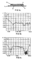
- Fig. 1 a shows an absorber 1 for incident electromagnetic energy in the microwave band, comprising a body adapted for mounting on a substrate by a first member in the form of a reflector 2 in the form of a metal sheet or plate, and a second member in the form of an electrically conductive member 3.
- the member 3 is a very thin conductive layer or film of plastic on one surface of which is deposited a conductive layer of vaporised aluminium. The coating is extremely thin and is therefore transparent.
- the reflector 2 is a base of the absorber.
- the conductive layer or film 3 is mounted or placed between two members 4 and 5, which are permeable to electromagnetic energy, in the form of clear acrylic plastic sheets.
- the body 1 is adapted by the metal sheet 2 for mounting on a substrate, and comprises a laminate.
- the thicknesses of the acrylic sheets 4, 5 and the conductivity of the aluminium layer or sheet 2 are selected for optimum performance.
- the absorber 1 is again a laminate.
- Fig. 1 b is a graph showing the measured absorption characteristics of an absorber 1 like that of Fig. 1 a .
- the reflector plate 2 was an aluminium sheet.
- the thicknesses of the sheets 4, 5 were adjusted to provide the best absorption levels over the frequency band from 8-18GHz, that is microwave frequencies.
- the curve shows that absorption levels of -20dB (1% reflected power) have been obtained over most of the frequency band.
- Fig. 1 c The effect of replacing the opaque aluiinium reflector 2 by a second transparent layer 3 also made from a vapourised metallic film is shown in Fig. 1 c .
- the metallic coating on this film was thicker and hence reflective to microwave energy whilst still having a high level of optical transparency. It is seen that a high level of microwave absorption of approximately -20dB has been obtained over the whole of mlcrowave band.
- the transmission characteristics of the absorber used in Fig. 1 b were measured on a IR Photospectrometer and are shown in Fig. 2. These measurements cover a wide IR waveband of 2.5 to 25 microns. It can be seen that the transmission through the test sheet is never greater than 2%. This indicates a high degree of reflec tivity over the whole of this band even when absorption is taken into account. The absorption is based on losses produced from multiple reflections from one or more thin conductive films.
- an absorber 1′ which is a symmetric absorber, in other words there is a reflector 2 which is placed centrally of the absorber with members 3, 4 and 5 on either side thereof, the members 4 and 5, as on the Fig.1 embodiment, each comprising a sheet of clear acrylic plastic permeable to electromagnetic energy and the member 3 being between the sheets 4 and 5 and comprising a very thin conductive layer or film of plastic on one surface of which is deposited a conductive layer of vaporised aluminium of such a thickness as to be effectively transparent.
- the absorber of Fig. 3 functions in the same way as that of Fig. 1.
- the aluminised sheet, or Bayfoil may be replaced in Figs. 1 a and 3 by a sputter deposited stainless steel as in Fig. 4 (see below).
- the non-conductive layer 2 may be replaced by non-conductive plastic foam, which provides a relatively light yet rigid absorber; the plastic sheets may be of polyvinyl chloride (pvc), polyester, or polyester fabric.
- the whole absorber may be enclosed in a sheath or envelope of fabric, such as polyester fabric, as shown at 6 in dashed lines in Fig. 3 forming a holder for the first and second members.
- the absorber shown schematically in Fig. 4 is a laminate of an outer cover comprising a sheet 8 of polyvinyl chloride (pvc), a top (as viewed) or inner sheet of pvc 9, a member 10 in the form of a sheet of foam material which is perforated with through perforations 10′ which are circular, of 12 mm diameter and which form a lattice or array 10 ⁇ in which there is a centre-to-centre spacing of 50 between adjacent orthogonally disposed apertures 10 a and a spacing of 35 mm, centre-to-centre, between diagonally disposed adjacent apertures 10 a , 10 b (see Fig. 5).
- pvc polyvinyl chloride
- 10′ which are circular, of 12 mm diameter and which form a lattice or array 10 ⁇ in which there is a centre-to-centre spacing of 50 between adjacent orthogonally disposed apertures 10 a and a spacing of 35 mm, centre-to-centre, between diagonally disposed adjacent apertures
- the foam 10 has a nominal thickness of 2.8 mm.
- the perforations 10′ assist in dissipation of incident electromagnetic energy in the microwave band, which energy is dissipated by the pores of the foam and absorbed by the perforations acting as 'wells' or 'sinks' in which the energy becomes absorbed.
- the perforations disrupt the electrical resistance, and, the foam with the other layers or sheets of the laminate provides an absorber which is harmonised electrically.
- the foam sheet 10 lies on a conductor in the form of a sheet 11 of material such as that sold under the trade name BAYFOIL, having a resistivity of approximately 350 ohms.
- Both foam sheets may be CN-120 foam, which is a closed cell conductive polyethylene foam.
- the conductor 11 in turn lies on a further sheet 12 of foam, in this case a solid or unperforated, foam, of nominal thickness about 2.2 mm.
- the foam sheet 12 in turn lies on a further sheet 13 of plastics material, preferably pvc and this in turn lies on a reflector sheet 14 such as an aluminised sheet of plastic, or a sheet of plastic with a sputter deposited stainless steel.
- a reflector sheet 14 such as an aluminised sheet of plastic, or a sheet of plastic with a sputter deposited stainless steel.
- the reflector 14 is then covered by a pvc outer cover or sheet 15.
- the outer covers or sheaths 8 and 15 can be secured together by any suitable means such as heat welding to form an envelope as shown in dashed lines in Fig. 3 which surrounds or encloses the whole absorber.
- the whole absorber 7 thus comprises a laminate of sheets 9-14, which absorber acts in a similar manner to that shown in Figs. 1 a and 3 in absorbing incident microwave energy in the microwave band, as well as acting as a reflector of heat energy so that the infra red energy cannot 'escape', and be detected, from a substrate to which the absorber is applied.
- the materials have a high reflectivity in the infra-red wavebands. This would enable them to belused both for shielding or deflection of infra-red energy. This property might be important for military use. Materials with this combination of features offer a very wide range of application particularly in the military field.
- a method of making the absorber can be used to convert sheets of many different types of plastic or other materials that allow microwaves to pass through them into efficient wide band absorbers.
- a feature of the method is that it can be applied to sheets of materials that are optically transparent. The sheets then acquire the properties of high absorption of microwaves whilst their optical performance is only slightly impaired.
- the materials are highly reflective and this feature provides secondary advantages as to heat protection.
Landscapes
- Laminated Bodies (AREA)
- Shielding Devices Or Components To Electric Or Magnetic Fields (AREA)
- Absorbent Articles And Supports Therefor (AREA)
- Crystals, And After-Treatments Of Crystals (AREA)
- Aerials With Secondary Devices (AREA)
- Materials For Medical Uses (AREA)
- Transition And Organic Metals Composition Catalysts For Addition Polymerization (AREA)
- Non-Silver Salt Photosensitive Materials And Non-Silver Salt Photography (AREA)
- Constitution Of High-Frequency Heating (AREA)
Applications Claiming Priority (4)
| Application Number | Priority Date | Filing Date | Title |
|---|---|---|---|
| GB8924084 | 1989-10-26 | ||
| GB898924084A GB8924084D0 (en) | 1989-10-26 | 1989-10-26 | Absorbers |
| GB9021027 | 1990-09-27 | ||
| GB909021027A GB9021027D0 (en) | 1989-10-26 | 1990-09-27 | Absorbers |
Publications (3)
| Publication Number | Publication Date |
|---|---|
| EP0425262A2 true EP0425262A2 (fr) | 1991-05-02 |
| EP0425262A3 EP0425262A3 (en) | 1991-10-30 |
| EP0425262B1 EP0425262B1 (fr) | 1995-06-21 |
Family
ID=26296108
Family Applications (1)
| Application Number | Title | Priority Date | Filing Date |
|---|---|---|---|
| EP19900311642 Expired - Lifetime EP0425262B1 (fr) | 1989-10-26 | 1990-10-24 | Absorbeurs |
Country Status (8)
| Country | Link |
|---|---|
| US (1) | US5225284A (fr) |
| EP (1) | EP0425262B1 (fr) |
| AT (1) | ATE124174T1 (fr) |
| DE (1) | DE69020301T2 (fr) |
| DK (1) | DK0425262T3 (fr) |
| ES (1) | ES2075167T3 (fr) |
| GB (1) | GB2239738B (fr) |
| GR (1) | GR3017423T3 (fr) |
Cited By (4)
| Publication number | Priority date | Publication date | Assignee | Title |
|---|---|---|---|---|
| WO1995000983A1 (fr) * | 1993-06-25 | 1995-01-05 | Nimtz Guenter | Agencement pour l'absorption d'ondes electromagnetiques et son procede de realisation |
| DE9408490U1 (de) * | 1994-05-25 | 1995-09-28 | Ernst Fehr technische Vertretungen und Beratung, Goldach | Strahlenschirmschutzauflage |
| FR2908560A1 (fr) * | 1991-11-25 | 2008-05-16 | Aerospatiale Soc Nat Ind Sa | Materiau composite structural a peau et un procede pour la fabrication de celui-ci |
| DE102008051028A1 (de) * | 2008-10-13 | 2010-04-15 | Nimtz, Günter, Prof. Dr. | Anordnung zur Absorption von elektromagnetischen Wellen und Absorberplatte |
Families Citing this family (4)
| Publication number | Priority date | Publication date | Assignee | Title |
|---|---|---|---|---|
| GB2608980B (en) * | 1990-08-21 | 2024-04-10 | Colebrand Ltd | A protection device |
| US6224982B1 (en) * | 1999-12-21 | 2001-05-01 | Lockhead Martin Corporation | Normal incidence multi-layer elastomeric radar absorber |
| US20040021597A1 (en) * | 2002-05-07 | 2004-02-05 | Dvorak George J. | Optimization of electromagnetic absorption in laminated composite plates |
| DE102008036500A1 (de) | 2008-08-05 | 2010-02-11 | Hans-Dieter Cornelius | Verfahren zur Herstellung eines graduierten Mikrowellenabsorbers |
Family Cites Families (32)
| Publication number | Priority date | Publication date | Assignee | Title |
|---|---|---|---|---|
| DE977551C (de) * | 1956-08-27 | 1966-12-22 | Eltro GmbH & Co Gesellschaft fur Strahlungstechnik, Heidelberg | Als Interferenzabsorber (Hochfrequenzabsorber) wirkende Dachpappe |
| DE977527C (de) * | 1956-08-31 | 1966-11-24 | Eltro G M B H & Co Ges Fuer St | Interferenzabsorber fuer Funkwellen als Radartarnung fuer Flugzeuge, Schiffe u. dgl. |
| DE977525C (de) * | 1956-08-31 | 1966-11-24 | Eltro G M B H & Co Ges Fuer St | Interferenzabsorber fuer Funkwellen als Radartarnung fuer Start- und Landebahnen |
| DE977522C (de) * | 1957-01-15 | 1966-11-03 | Eltro G M B H & Co Ges Fuer St | Verpackungsmaterial in Form von Behaeltern mit Interferenzabsorption fuer elektromagnetische Wellen |
| NL112646C (fr) * | 1958-12-04 | |||
| NL242147A (fr) * | 1959-07-03 | |||
| US4012738A (en) * | 1961-01-31 | 1977-03-15 | The United States Of America As Represented By The Secretary Of The Navy | Combined layers in a microwave radiation absorber |
| US3526896A (en) * | 1961-02-02 | 1970-09-01 | Ludwig Wesch | Resonance absorber for electromagnetic waves |
| US3887920A (en) * | 1961-03-16 | 1975-06-03 | Us Navy | Thin, lightweight electromagnetic wave absorber |
| US3938152A (en) * | 1963-06-03 | 1976-02-10 | Mcdonnell Douglas Corporation | Magnetic absorbers |
| US4924228A (en) * | 1963-07-17 | 1990-05-08 | Boeing Company | Aircraft construction |
| US4024318A (en) * | 1966-02-17 | 1977-05-17 | Exxon Research And Engineering Company | Metal-filled plastic material |
| US4173018A (en) * | 1967-07-27 | 1979-10-30 | Whittaker Corporation | Anti-radar means and techniques |
| US4170010A (en) * | 1968-03-04 | 1979-10-02 | Rockwell International Corporation | Inflatable radiation attenuator |
| DE1916326A1 (de) * | 1968-04-01 | 1969-10-30 | Barracudaverken Ab | Tarnungsmittel zum Verhindern oder Hemmen der Entdeckung durch Radarerkundung |
| US4006479A (en) * | 1969-02-04 | 1977-02-01 | The United States Of America As Represented By The Secretary Of The Air Force | Method for dispersing metallic particles in a dielectric binder |
| US3568196A (en) * | 1969-02-06 | 1971-03-02 | Raytheon Co | Radio frequency absorber |
| US4084161A (en) * | 1970-05-26 | 1978-04-11 | The United States Of America As Represented By The Secretary Of The Army | Heat resistant radar absorber |
| US3721982A (en) * | 1970-11-10 | 1973-03-20 | Gruenzweig & Hartmann | Absorber for electromagnetic radiation |
| GB1450791A (en) * | 1973-05-18 | 1976-09-29 | Vickers Ltd | Sound absorbing materials |
| GB1540829A (en) * | 1975-04-15 | 1979-02-14 | Lucas Industries Ltd | Method of manufacturing a recessed structure |
| US4038660A (en) * | 1975-08-05 | 1977-07-26 | The United States Of America As Represented By The Secretary Of The Army | Microwave absorbers |
| GB2163296B (en) * | 1977-09-01 | 1986-08-13 | Elliott Bros | Reducing radar reflections |
| US4522890A (en) * | 1979-10-31 | 1985-06-11 | Illinois Tool Works Inc. | Multilayer high attenuation shielding structure |
| SE8007075L (sv) * | 1979-10-31 | 1981-05-01 | Illinois Tool Works | Skermning |
| US4386354A (en) * | 1980-12-15 | 1983-05-31 | Plessey Overseas Limited | Electromagnetic noise suppression |
| US4480256A (en) * | 1981-08-18 | 1984-10-30 | The Boeing Company | Microwave absorber |
| JPS58169997A (ja) * | 1982-03-31 | 1983-10-06 | 日本カ−ボン株式会社 | 電波吸収体 |
| DE3534059C1 (en) * | 1985-09-25 | 1990-05-17 | Dornier Gmbh | Fibre composite material |
| US4726980A (en) * | 1986-03-18 | 1988-02-23 | Nippon Carbon Co., Ltd. | Electromagnetic wave absorbers of silicon carbide fibers |
| JPH0650799B2 (ja) * | 1986-11-19 | 1994-06-29 | 喜之 内藤 | 電波吸収材 |
| US4814546A (en) * | 1987-11-25 | 1989-03-21 | Minnesota Mining And Manufacturing Company | Electromagnetic radiation suppression cover |
-
1990
- 1990-10-24 DE DE69020301T patent/DE69020301T2/de not_active Expired - Fee Related
- 1990-10-24 DK DK90311642T patent/DK0425262T3/da active
- 1990-10-24 AT AT90311642T patent/ATE124174T1/de active
- 1990-10-24 ES ES90311642T patent/ES2075167T3/es not_active Expired - Lifetime
- 1990-10-24 GB GB9023194A patent/GB2239738B/en not_active Revoked
- 1990-10-24 EP EP19900311642 patent/EP0425262B1/fr not_active Expired - Lifetime
- 1990-10-25 US US07/603,240 patent/US5225284A/en not_active Expired - Fee Related
-
1995
- 1995-09-14 GR GR950402543T patent/GR3017423T3/el unknown
Cited By (6)
| Publication number | Priority date | Publication date | Assignee | Title |
|---|---|---|---|---|
| FR2908560A1 (fr) * | 1991-11-25 | 2008-05-16 | Aerospatiale Soc Nat Ind Sa | Materiau composite structural a peau et un procede pour la fabrication de celui-ci |
| WO1995000983A1 (fr) * | 1993-06-25 | 1995-01-05 | Nimtz Guenter | Agencement pour l'absorption d'ondes electromagnetiques et son procede de realisation |
| US5710564A (en) * | 1993-06-25 | 1998-01-20 | Nimtz; Guenter | System for absorbing electromagnetic waves and method of manufacturing this system |
| CN1054473C (zh) * | 1993-06-25 | 2000-07-12 | 古温特·尼姆兹 | 吸收电磁波的系统及制造该系统的方法 |
| DE9408490U1 (de) * | 1994-05-25 | 1995-09-28 | Ernst Fehr technische Vertretungen und Beratung, Goldach | Strahlenschirmschutzauflage |
| DE102008051028A1 (de) * | 2008-10-13 | 2010-04-15 | Nimtz, Günter, Prof. Dr. | Anordnung zur Absorption von elektromagnetischen Wellen und Absorberplatte |
Also Published As
| Publication number | Publication date |
|---|---|
| ATE124174T1 (de) | 1995-07-15 |
| DE69020301D1 (de) | 1995-07-27 |
| DE69020301T2 (de) | 1996-02-08 |
| GB2239738B (en) | 1994-10-19 |
| GR3017423T3 (en) | 1995-12-31 |
| EP0425262B1 (fr) | 1995-06-21 |
| GB9023194D0 (en) | 1990-12-05 |
| DK0425262T3 (da) | 1995-10-30 |
| ES2075167T3 (es) | 1995-10-01 |
| EP0425262A3 (en) | 1991-10-30 |
| GB2239738A (en) | 1991-07-10 |
| US5225284A (en) | 1993-07-06 |
Similar Documents
| Publication | Publication Date | Title |
|---|---|---|
| US8643531B2 (en) | Electromagnetic wave absorber | |
| US5400043A (en) | Absorptive/transmissive radome | |
| US5583318A (en) | Multi-layer shield for absorption of electromagnetic energy | |
| EP0425262B1 (fr) | Absorbeurs | |
| US5373102A (en) | Optically transmissive Faraday cage | |
| JPS61140203A (ja) | 抵抗性ループ角度フイルタ | |
| AU599529B2 (en) | Shielding membrane | |
| CA2110601A1 (fr) | Membrane pare-soleil transparente au rayonnement radiofrequence pour antenne | |
| CN113165339A (zh) | 导电性非织造布 | |
| WO2021199920A1 (fr) | Film d'adaptation d'impédance et absorbeur d'ondes radio | |
| CN1262792A (zh) | 带有辐射吸收装置的手提式电话 | |
| US5358787A (en) | RF absorptive window | |
| US6700525B2 (en) | Radiation absorber | |
| WO1992001319A1 (fr) | Plaque zonale reflechissante de correction de phase servant a concentrer des micro-ondes | |
| CN117908172A (zh) | 一种宽带红外辐射全方位定向控制器及其设计方法 | |
| GB2277200A (en) | A cover for a spacecraft antenna | |
| WO2023033011A1 (fr) | Blindage contre les ondes électromagnétiques | |
| WO2021199921A1 (fr) | Absorbeur d'ondes radio | |
| JP7559986B2 (ja) | 高周波拡散シート | |
| WO2020189350A1 (fr) | Absorbeur d'ondes électromagnétiques et kit d'absorbeur d'ondes électromagnétiques | |
| US20260025964A1 (en) | Electromagnetic wave absorbing member | |
| JP7515765B1 (ja) | 導電性筐体及び電磁波加熱装置 | |
| US20250210877A1 (en) | Reflective panel, electromagnetic wave reflecting apparatus using reflective panel, electromagnetic wave reflecting fence, and method of making reflective panel | |
| JP2024104865A (ja) | Cバンド電磁波吸収体 | |
| CN121941667A (zh) | 窗材及窗材的制造方法 |
Legal Events
| Date | Code | Title | Description |
|---|---|---|---|
| PUAI | Public reference made under article 153(3) epc to a published international application that has entered the european phase |
Free format text: ORIGINAL CODE: 0009012 |
|
| AK | Designated contracting states |
Kind code of ref document: A2 Designated state(s): AT BE CH DE DK ES FR GB GR IT LI LU NL SE |
|
| PUAL | Search report despatched |
Free format text: ORIGINAL CODE: 0009013 |
|
| AK | Designated contracting states |
Kind code of ref document: A3 Designated state(s): AT BE CH DE DK ES FR GB GR IT LI LU NL SE |
|
| 17P | Request for examination filed |
Effective date: 19920324 |
|
| 17Q | First examination report despatched |
Effective date: 19931206 |
|
| GRAA | (expected) grant |
Free format text: ORIGINAL CODE: 0009210 |
|
| AK | Designated contracting states |
Kind code of ref document: B1 Designated state(s): AT BE CH DE DK ES FR GB GR IT LI LU NL SE |
|
| REF | Corresponds to: |
Ref document number: 124174 Country of ref document: AT Date of ref document: 19950715 Kind code of ref document: T |
|
| REF | Corresponds to: |
Ref document number: 69020301 Country of ref document: DE Date of ref document: 19950727 |
|
| ITF | It: translation for a ep patent filed | ||
| REG | Reference to a national code |
Ref country code: ES Ref legal event code: FG2A Ref document number: 2075167 Country of ref document: ES Kind code of ref document: T3 |
|
| ET | Fr: translation filed | ||
| REG | Reference to a national code |
Ref country code: DK Ref legal event code: T3 |
|
| REG | Reference to a national code |
Ref country code: GR Ref legal event code: FG4A Free format text: 3017423 |
|
| PLBE | No opposition filed within time limit |
Free format text: ORIGINAL CODE: 0009261 |
|
| STAA | Information on the status of an ep patent application or granted ep patent |
Free format text: STATUS: NO OPPOSITION FILED WITHIN TIME LIMIT |
|
| 26N | No opposition filed | ||
| PGFP | Annual fee paid to national office [announced via postgrant information from national office to epo] |
Ref country code: LU Payment date: 19961001 Year of fee payment: 7 |
|
| PGFP | Annual fee paid to national office [announced via postgrant information from national office to epo] |
Ref country code: AT Payment date: 19961011 Year of fee payment: 7 |
|
| PGFP | Annual fee paid to national office [announced via postgrant information from national office to epo] |
Ref country code: DK Payment date: 19961025 Year of fee payment: 7 |
|
| PGFP | Annual fee paid to national office [announced via postgrant information from national office to epo] |
Ref country code: BE Payment date: 19961212 Year of fee payment: 7 |
|
| PGFP | Annual fee paid to national office [announced via postgrant information from national office to epo] |
Ref country code: FR Payment date: 19971009 Year of fee payment: 8 |
|
| PGFP | Annual fee paid to national office [announced via postgrant information from national office to epo] |
Ref country code: SE Payment date: 19971015 Year of fee payment: 8 |
|
| PG25 | Lapsed in a contracting state [announced via postgrant information from national office to epo] |
Ref country code: LU Free format text: LAPSE BECAUSE OF NON-PAYMENT OF DUE FEES Effective date: 19971024 Ref country code: AT Free format text: LAPSE BECAUSE OF NON-PAYMENT OF DUE FEES Effective date: 19971024 |
|
| PGFP | Annual fee paid to national office [announced via postgrant information from national office to epo] |
Ref country code: GR Payment date: 19971024 Year of fee payment: 8 |
|
| REG | Reference to a national code |
Ref country code: DK Ref legal event code: EBP |
|
| PGFP | Annual fee paid to national office [announced via postgrant information from national office to epo] |
Ref country code: NL Payment date: 19971029 Year of fee payment: 8 |
|
| PG25 | Lapsed in a contracting state [announced via postgrant information from national office to epo] |
Ref country code: DK Free format text: LAPSE BECAUSE OF NON-PAYMENT OF DUE FEES Effective date: 19971031 Ref country code: BE Free format text: LAPSE BECAUSE OF NON-PAYMENT OF DUE FEES Effective date: 19971031 |
|
| PGFP | Annual fee paid to national office [announced via postgrant information from national office to epo] |
Ref country code: ES Payment date: 19971031 Year of fee payment: 8 Ref country code: DE Payment date: 19971031 Year of fee payment: 8 |
|
| PGFP | Annual fee paid to national office [announced via postgrant information from national office to epo] |
Ref country code: CH Payment date: 19971106 Year of fee payment: 8 |
|
| BERE | Be: lapsed |
Owner name: COLEBRAND LTD Effective date: 19971031 |
|
| PG25 | Lapsed in a contracting state [announced via postgrant information from national office to epo] |
Ref country code: SE Free format text: LAPSE BECAUSE OF NON-PAYMENT OF DUE FEES Effective date: 19981025 |
|
| PG25 | Lapsed in a contracting state [announced via postgrant information from national office to epo] |
Ref country code: ES Free format text: LAPSE BECAUSE OF THE APPLICANT RENOUNCES Effective date: 19981026 |
|
| PG25 | Lapsed in a contracting state [announced via postgrant information from national office to epo] |
Ref country code: LI Free format text: LAPSE BECAUSE OF NON-PAYMENT OF DUE FEES Effective date: 19981031 Ref country code: GR Free format text: LAPSE BECAUSE OF NON-PAYMENT OF DUE FEES Effective date: 19981031 Ref country code: CH Free format text: LAPSE BECAUSE OF NON-PAYMENT OF DUE FEES Effective date: 19981031 |
|
| PG25 | Lapsed in a contracting state [announced via postgrant information from national office to epo] |
Ref country code: NL Free format text: LAPSE BECAUSE OF NON-PAYMENT OF DUE FEES Effective date: 19990501 |
|
| REG | Reference to a national code |
Ref country code: CH Ref legal event code: PL |
|
| EUG | Se: european patent has lapsed |
Ref document number: 90311642.4 |
|
| PG25 | Lapsed in a contracting state [announced via postgrant information from national office to epo] |
Ref country code: FR Free format text: LAPSE BECAUSE OF NON-PAYMENT OF DUE FEES Effective date: 19990630 |
|
| NLV4 | Nl: lapsed or anulled due to non-payment of the annual fee |
Effective date: 19990501 |
|
| REG | Reference to a national code |
Ref country code: FR Ref legal event code: ST |
|
| PG25 | Lapsed in a contracting state [announced via postgrant information from national office to epo] |
Ref country code: DE Free format text: LAPSE BECAUSE OF NON-PAYMENT OF DUE FEES Effective date: 19990803 |
|
| PGFP | Annual fee paid to national office [announced via postgrant information from national office to epo] |
Ref country code: GB Payment date: 19991020 Year of fee payment: 10 |
|
| PG25 | Lapsed in a contracting state [announced via postgrant information from national office to epo] |
Ref country code: GB Free format text: LAPSE BECAUSE OF NON-PAYMENT OF DUE FEES Effective date: 20001024 |
|
| REG | Reference to a national code |
Ref country code: ES Ref legal event code: FD2A Effective date: 20001102 |
|
| GBPC | Gb: european patent ceased through non-payment of renewal fee |
Effective date: 20001024 |
|
| PG25 | Lapsed in a contracting state [announced via postgrant information from national office to epo] |
Ref country code: IT Free format text: LAPSE BECAUSE OF NON-PAYMENT OF DUE FEES;WARNING: LAPSES OF ITALIAN PATENTS WITH EFFECTIVE DATE BEFORE 2007 MAY HAVE OCCURRED AT ANY TIME BEFORE 2007. THE CORRECT EFFECTIVE DATE MAY BE DIFFERENT FROM THE ONE RECORDED. Effective date: 20051024 |