EP0425516B1 - Transversal einmodiger, auf stoss an die pump-diode gekoppelter laser - Google Patents
Transversal einmodiger, auf stoss an die pump-diode gekoppelter laser Download PDFInfo
- Publication number
- EP0425516B1 EP0425516B1 EP89906946A EP89906946A EP0425516B1 EP 0425516 B1 EP0425516 B1 EP 0425516B1 EP 89906946 A EP89906946 A EP 89906946A EP 89906946 A EP89906946 A EP 89906946A EP 0425516 B1 EP0425516 B1 EP 0425516B1
- Authority
- EP
- European Patent Office
- Prior art keywords
- laser
- optical
- diode
- radiation
- laser gain
- Prior art date
- Legal status (The legal status is an assumption and is not a legal conclusion. Google has not performed a legal analysis and makes no representation as to the accuracy of the status listed.)
- Expired - Lifetime
Links
Images
Classifications
-
- H—ELECTRICITY
- H01—ELECTRIC ELEMENTS
- H01S—DEVICES USING THE PROCESS OF LIGHT AMPLIFICATION BY STIMULATED EMISSION OF RADIATION [LASER] TO AMPLIFY OR GENERATE LIGHT; DEVICES USING STIMULATED EMISSION OF ELECTROMAGNETIC RADIATION IN WAVE RANGES OTHER THAN OPTICAL
- H01S3/00—Lasers, i.e. devices using stimulated emission of electromagnetic radiation in the infrared, visible or ultraviolet wave range
- H01S3/05—Construction or shape of optical resonators; Accommodation of active medium therein; Shape of active medium
- H01S3/06—Construction or shape of active medium
- H01S3/0627—Construction or shape of active medium the resonator being monolithic, e.g. microlaser
-
- H—ELECTRICITY
- H01—ELECTRIC ELEMENTS
- H01S—DEVICES USING THE PROCESS OF LIGHT AMPLIFICATION BY STIMULATED EMISSION OF RADIATION [LASER] TO AMPLIFY OR GENERATE LIGHT; DEVICES USING STIMULATED EMISSION OF ELECTROMAGNETIC RADIATION IN WAVE RANGES OTHER THAN OPTICAL
- H01S3/00—Lasers, i.e. devices using stimulated emission of electromagnetic radiation in the infrared, visible or ultraviolet wave range
- H01S3/02—Constructional details
- H01S3/04—Arrangements for thermal management
- H01S3/042—Arrangements for thermal management for solid state lasers
-
- H—ELECTRICITY
- H01—ELECTRIC ELEMENTS
- H01S—DEVICES USING THE PROCESS OF LIGHT AMPLIFICATION BY STIMULATED EMISSION OF RADIATION [LASER] TO AMPLIFY OR GENERATE LIGHT; DEVICES USING STIMULATED EMISSION OF ELECTROMAGNETIC RADIATION IN WAVE RANGES OTHER THAN OPTICAL
- H01S3/00—Lasers, i.e. devices using stimulated emission of electromagnetic radiation in the infrared, visible or ultraviolet wave range
- H01S3/09—Processes or apparatus for excitation, e.g. pumping
- H01S3/091—Processes or apparatus for excitation, e.g. pumping using optical pumping
- H01S3/094—Processes or apparatus for excitation, e.g. pumping using optical pumping by coherent light
- H01S3/0941—Processes or apparatus for excitation, e.g. pumping using optical pumping by coherent light of a laser diode
- H01S3/09415—Processes or apparatus for excitation, e.g. pumping using optical pumping by coherent light of a laser diode the pumping beam being parallel to the lasing mode of the pumped medium, e.g. end-pumping
-
- H—ELECTRICITY
- H01—ELECTRIC ELEMENTS
- H01S—DEVICES USING THE PROCESS OF LIGHT AMPLIFICATION BY STIMULATED EMISSION OF RADIATION [LASER] TO AMPLIFY OR GENERATE LIGHT; DEVICES USING STIMULATED EMISSION OF ELECTROMAGNETIC RADIATION IN WAVE RANGES OTHER THAN OPTICAL
- H01S3/00—Lasers, i.e. devices using stimulated emission of electromagnetic radiation in the infrared, visible or ultraviolet wave range
- H01S3/10—Controlling the intensity, frequency, phase, polarisation or direction of the emitted radiation, e.g. switching, gating, modulating or demodulating
- H01S3/106—Controlling the intensity, frequency, phase, polarisation or direction of the emitted radiation, e.g. switching, gating, modulating or demodulating by controlling devices placed within the cavity
- H01S3/108—Controlling the intensity, frequency, phase, polarisation or direction of the emitted radiation, e.g. switching, gating, modulating or demodulating by controlling devices placed within the cavity using non-linear optical devices, e.g. exhibiting Brillouin or Raman scattering
- H01S3/109—Frequency multiplication, e.g. harmonic generation
-
- G—PHYSICS
- G01—MEASURING; TESTING
- G01N—INVESTIGATING OR ANALYSING MATERIALS BY DETERMINING THEIR CHEMICAL OR PHYSICAL PROPERTIES
- G01N2291/00—Indexing codes associated with group G01N29/00
- G01N2291/26—Scanned objects
- G01N2291/269—Various geometry objects
- G01N2291/2691—Bolts, screws, heads
-
- H—ELECTRICITY
- H01—ELECTRIC ELEMENTS
- H01S—DEVICES USING THE PROCESS OF LIGHT AMPLIFICATION BY STIMULATED EMISSION OF RADIATION [LASER] TO AMPLIFY OR GENERATE LIGHT; DEVICES USING STIMULATED EMISSION OF ELECTROMAGNETIC RADIATION IN WAVE RANGES OTHER THAN OPTICAL
- H01S3/00—Lasers, i.e. devices using stimulated emission of electromagnetic radiation in the infrared, visible or ultraviolet wave range
- H01S3/02—Constructional details
- H01S3/025—Constructional details of solid state lasers, e.g. housings or mountings
-
- H—ELECTRICITY
- H01—ELECTRIC ELEMENTS
- H01S—DEVICES USING THE PROCESS OF LIGHT AMPLIFICATION BY STIMULATED EMISSION OF RADIATION [LASER] TO AMPLIFY OR GENERATE LIGHT; DEVICES USING STIMULATED EMISSION OF ELECTROMAGNETIC RADIATION IN WAVE RANGES OTHER THAN OPTICAL
- H01S3/00—Lasers, i.e. devices using stimulated emission of electromagnetic radiation in the infrared, visible or ultraviolet wave range
- H01S3/02—Constructional details
- H01S3/04—Arrangements for thermal management
- H01S3/0405—Conductive cooling, e.g. by heat sinks or thermo-electric elements
-
- H—ELECTRICITY
- H01—ELECTRIC ELEMENTS
- H01S—DEVICES USING THE PROCESS OF LIGHT AMPLIFICATION BY STIMULATED EMISSION OF RADIATION [LASER] TO AMPLIFY OR GENERATE LIGHT; DEVICES USING STIMULATED EMISSION OF ELECTROMAGNETIC RADIATION IN WAVE RANGES OTHER THAN OPTICAL
- H01S3/00—Lasers, i.e. devices using stimulated emission of electromagnetic radiation in the infrared, visible or ultraviolet wave range
- H01S3/05—Construction or shape of optical resonators; Accommodation of active medium therein; Shape of active medium
- H01S3/06—Construction or shape of active medium
- H01S3/0602—Crystal lasers or glass lasers
- H01S3/0604—Crystal lasers or glass lasers in the form of a plate or disc
-
- H—ELECTRICITY
- H01—ELECTRIC ELEMENTS
- H01S—DEVICES USING THE PROCESS OF LIGHT AMPLIFICATION BY STIMULATED EMISSION OF RADIATION [LASER] TO AMPLIFY OR GENERATE LIGHT; DEVICES USING STIMULATED EMISSION OF ELECTROMAGNETIC RADIATION IN WAVE RANGES OTHER THAN OPTICAL
- H01S3/00—Lasers, i.e. devices using stimulated emission of electromagnetic radiation in the infrared, visible or ultraviolet wave range
- H01S3/05—Construction or shape of optical resonators; Accommodation of active medium therein; Shape of active medium
- H01S3/08—Construction or shape of optical resonators or components thereof
- H01S3/08018—Mode suppression
- H01S3/0804—Transverse or lateral modes
- H01S3/08045—Single-mode emission
Definitions
- the present invention relates in general to diode pumped solid state lasers and, more particularly, to an improved laser wherein the diode pump is butt-coupled to the laser gain material.
- the pumping radiation emanating from the output facet of the diode pump has a cone of divergence falling within the range of 30° to 40°.
- the pumping light pumps a relatively large mode volume of the laser gain material.
- the sides of the laser rod were polished for internally reflecting the pumping radiation back into the rod so that the pumping radiation would essentially pump the entire volume of the rod, which was approximately 2,54 cm (1") in length.
- the pumped mode volume is sufficiently large in transverse cross-sectional area to support higher order transverse modes of oscillation within the laser cavity.
- the output of the laser will not be a single transverse mode but will include higher order modes. It is desirable to obtain a single transverse mode of operation on the fundamental TEM00 mode.
- imaging elements between the pumping diode and the laser gain medium increases the complexity of the diode pumped laser.
- Two alignment operations are necessary to produce laser action.
- the imaging or focusing element must be properly aligned with respect to the output facet of the laser diode and, secondly, the solid state laser gain medium must be properly aligned with the diode-lens combination. Both of these operations require motion along three orthogonal axes. It is desirable to eliminate the cost and complexity of the alignment mechanisms.
- the diode pumped fiber lasers can utilize butt-coupling techniques.
- the fabrication of fiber lasers requires highly complex crystal growth and polishing techniques.
- the principal object of the present invention is the provision of an improved single transverse mode diode pumped laser.
- the diode pumped solid state laser according to the present invention is defined in claim 14.
- the method for obtaining single transverse mode with the laser of the present invention is defined in claim 1.
- the output facet of the diode pump is butt-coupled (closely coupled) to an input facet of the laser gain medium and the laser gain medium is selected to have a very short absorption length for the optical pumping radiation, i.e., less than 500 micrometers, such that a sufficiently small volume of laser gain material is pumped so as to excite essentially only a single transverse mode of laser oscillation within the laser gain medium and optical resonator containing same.
- the output reflector for a diode laser pump and the input reflector for a solid state laser are coated on a common surface, either the output facet of the diode or the input facet of the solid state laser, whereby back reflections are eliminated which can produce amplitude and frequency instabilities of the solid state laser.
- the output facet of the diode pump is butt-coupled to an input facet of the laser gain material by a layer of an index-matching optical adhesive, whereby the size and complexity of the resultant laser is substantially reduced.
- the laser gain medium includes parallel planar input and output faces with the output face having a reflective coating deposited thereon to form the output mirror of an optical resonator containing the laser gain medium, whereby the laser gain medium comprises a Fabry-Perot cavity and the resultant laser is of reduced size and complexity.
- an optically transparent member is fixedly secured to the laser gain medium and an output facet of said optically transparent member is coated to provide one of the reflectors of the laser cavity containing the laser gain medium, whereby the size and construction of the laser is reduced in use.
- an optically non-linear member is fixedly secured to the laser gain medium with an output facet of the non-linear material being coated to define an output mirror of the laser cavity, whereby a harmonic generator is obtained of reduced size and complexity.
- an optically transparent member is fixedly secured to the laser gain medium and coated with a reflective coating to define an output mirror of the laser cavity.
- the optically transparent member is made of a material having a temperature coefficient of optical pathlength therethrough of opposite sign to that of the laser gain medium, whereby the overall temperature coefficient for the output frequency of the laser is reduced in use.
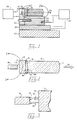
- a diode pumped solid state laser incorporating features of the present invention is denoted 11 as a whole.
- a slab of laser gain material 12 having input and output broad faces 13 and 14 has mounted thereto, in closely spaced relation, an optically transparent rod 15, such as fused quartz.
- the fused quartz member 15 has an input face 16 and an output face 17.
- the output face is curved with a radius of curvature of about one centimeter and is coated with an optical coating to form the output mirror of an optical resonator defined between mirror surface 17 and the input face 13 of the laser gain medium 12 which has been similarly coated with a coating to be optically reflective at the laser wavelength.
- An optical pumping diode 18 has its output facet 19 disposed in butt-coupled relationship to the input facet 13 of the laser gain medium.
- butt-coupled is defined to mean a coupling sufficiently close, i.e., less than 25 micrometres (0.001"), such that the divergent beam of optical pumping radiation emanating from the output facet 19, and essentially on the optical axis of the laser resonator, will optically pump a mode volume within the medium with sufficiently small transverse cross-sectional area to support essentially only single transverse mode laser operation, i.e., Tem00 mode operation.
- the laser gain medium 12 has a relatively short absorption length for the pumping radiation, i.e., 63% of the optical pumping radiation passing through the input facet 13 is absorbed within a pathlength of less than 500 microns within the laser gain medium.
- the absorption length is chosen and the spacing between the output facet 19 of the pumping diode 18 is chosen such that the pumped mode volume within the gain medium 12 has a transverse cross-sectional area sufficiently small to support laser oscillation on only a single transverse mode, i.e., Tem00 mode.
- the divergent lobe of pumping radiation is aligned to be essentially collinear with the optical axis of the optical resonator defined between mirrors 13 and 17.
- the optically transparent member 15 is fixedly secured to the output face 14 of the gain medium 12 by means of a suitable adhesive bead at 21.
- the diode pump is fixedly secured to a mounting member 22, as of copper, which in turn is screwed, or otherwise fixedly attached, to a mounting block 23, such as copper.
- the laser gain medium 12 and the optically transparent rod 15 are fixedly secured to the mounting block by an adhesive.
- Thermoelectric cooler 24 maintains mounting blocks 22 and 23 at a desired temperature.
- the hot face of thermoelectric cooler 24 is mounted in heat-exchanging relation to a heat sink 25.
- a temperature sensor 26, such as a thermistor is mounted within mounting block 23 for sensing its temperature.
- a diode pump power supply 28 supplies current to the diode pump 18.
- diode pump 18 is a laser diode of the single-stripe type, either gain or index guided, with output power in the range of 5 to 40 mW.
- the output frequency of the diode pump 18 is matched to a strong absorption line in the solid state gain medium 12 by varying the temperature and/or current supplied to it.
- the diode current may be constant in value or modulated to produce relaxation or spike-mode oscillations in the solid state laser.
- a suitable laser diode 18 is the SDL-1400-C manufactured by Spectra Diode Labs of San Jose, California.
- a suitable temperature controller 27 is disclosed in Electronics Device News, June 20, 1977, pg. 90, Fig. 6, and a suitable thermoelectric cooler 24 is the Frigichip Model FC-0.6-32-06L, commercially available from Melcor Industries.
- a typical example of the laser gain medium 12 is one having an absorption length for the diode pumping radiation of less than 75 microns and is polished flat and parallel on faces 13 and 14 to accuracies typical of intra-cavity laser optics. Thicknesses of the gain material 12 may vary from 0.1 to 2 millimeters.
- a dielectric reflecting coating is applied to input face 13 which transmits greater than 85% of the diode pumping radiation and reflects more than 99.5% of the laser radiation emanating within the gain medium 12.
- the output face 14 of the gain medium 12 is coated with a dielectric anti-reflection coating optimized for the lasant wavelength emanating from the gain medium 12. Transmission of radiation through the output face 14 should exceed 99.5% for the lasant radiation emanating within the member 12.
- the optically transparent member 15 is also polished to tolerances typical for intra-cavity laser optics. Its input face 16 is flat and is coated with an anti-reflection coating which transmits greater than 99.5% at the lasant wavelength emanating from the gain medium 12. Its output face 17 is polished convex with a radius of curvature from 5 to 40 millimeters and coated with a dielectric coating which reflects 98% to 99.8% of the lasant radiation emanating from the gain medium 12. Gain medium 12 and optically transparent member 15 are fixed together in a rigid housing or alternatively fastened together with a suitable adhesive at 21. Preferably, there is a gap exceeding 10 microns in width between the output face 14 of the gain medium and the input face 16 of the optically transparent member 15.
- the laser gain medium 12 comprises a lithium neodymium tetraphosphate crystal, 1 millimeter thick by 2 millimeters square cross-section.
- the planar faces 13 and 14 are parallel to better than 10 arc seconds. The surface is polished to a polish figure greater than 1/10th of a wavelength.
- the input face 13 has a reflectivity greater than 99.9% at 1.32 microns with transmission greater than 90% at 800 nanometers, i.e., the pump wavelength.
- the output face 14 of the gain medium 12 has an anti-reflective coating for 1.32 microns wavelength and its transmission at that wavelength exceeds 99.8%.
- the optically transparent member 15 is a rod three millimeters in length and three millimeters in cross-sectional diameter.
- Its input face 16 is flat and its output face 17 has a one centimeter convex radius of curvature.
- Rod 15 is polished to a finish better than 1/10th of a wavelength.
- the input face 16 is perpendicular to better than one minute and the curvature of the output face 17 is centered to better than thirty microns.
- the input face 16 has an antireflective coating for radiation of a wavelength of 1.32 microns and is transmissive to in excess of 99.8% at 1.32 microns.
- the output face 17 has a reflective coating which reflects 99.7% at the laser wavelength of 1.32 microns. In the laser of Fig.
- the pumping radiation should be absorbed within a small distance from the input facet 13 and within the gain medium 12. In such a case, energy is transferred to the laser gain medium before significant divergence of the pump beam can take place.
- back reflection of the diode pump radiation from the input facet 13 of the laser gain medium 12 is shown at 31 and back reflection of solid state laser radiation emanating from the gain medium and reflecting from the diode output facet 19 is shown at 32.
- These two sources of back reflection are significant causes of amplitude and frequency instability in the output of the solid state laser at 33. These amplitude and frequency instabilities are dependent on the intensity and phase of the radiation reflected back into the output facet 19 of the diode pump.
- Semiconductor laser diode pumps 18 are especially sensitive to this form of perturbation due to a combination of high gain and large output coupling. Diode fluctuations produce relaxation oscillations in the solid state laser 12 which appear as a sinusoidal modulation on the output beam 33.
- Back reflections from the solid state gain medium at 32 also produce instabilities but the situation is somewhat better in that the input face 13 of gain medium is a high reflector at the laser wavelength.
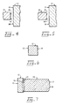
- FIG. 4 An alternative embodiment of the present invention in which undesired back reflections are eliminated is shown in Fig. 4. More particularly, in the embodiment of Fig. 4, the output reflector for the diode laser 18 and the input reflector for the gain medium 12 are coated on a common surface, either the diode facet 19 or the input facet 13 of the gain medium 12.
- the diode output facet 19 has a dielectric coating applied to it with reflectivity between 0% and 70% at the diode pumping wavelength at 99% to 99.9% at the lasant wavelength of the laser gain medium. The exact value of the diode reflectivity depends on the optimum value for the particular diode being used.
- Front facet 13 of the solid state gain medium 12 is anti-reflective coated for both wavelengths, i.e., pump and laser so that the transmission exceeds 99%.
- the coatings are reversed relative to the embodiment of Fig. 4. More particularly, the common reflectors are coated on the input facet 13 of the gain medium and the anti-reflection coatings are applied to the output facet 19 of the diode 18. Reflectivity values are identical to those of the embodiment of Fig. 4 and the distance between the output facet 19 and the input facet 13, in this case, must be less, than 10 micrometers.
- Figs. 4 and 5 eliminate back reflections since the diode radiation is absorbed before it can be reflected by the laser gain medium and for most wavelengths, the same is true for the laser radiation emanating from the laser gain medium.
- the output facet 19 of the pumping diode 18 and the input facet 13 of the laser gain medium 12 may be bonded together by a suitable optical adhesive.
- the optical adhesive is index matching for the diode index of refraction and the gain material index of refraction and fills the space between the facets 19 and 13.
- the antireflection coatings may be eliminated.
- utilizing the optical cement a compact composite structure is obtained which is advantageous from the standpoint of device stability. In addition, the size of the device is reduced.
- Fig. 6 there is shown an alternative embodiment wherein the laser gain medium 12 has reflectors formed on opposite major faces of the medium at 13 and 14 to define a Fabry-Perot optical resonator.
- Input face 13 of the gain medium is coated to be highly reflective for the laser radiation emanating within the member 15 and highly transmissive for the pump radiation passing through the input facet 13.
- the output facet 14 is coated for 98% to 99.9% reflectivity at the wavelength of the laser radiation emanating from the gain medium.
- the common mirror embodiments of Figs. 4 and 5 are achieved.
- lasers are obtained which are not much larger than the pump diodes themselves.
- FIG. 7 A harmonic generator incorporating features of the present invention is shown in Fig. 7. More particularly, the structure of Fig. 7 is essentially the same as that previously described with regard to Fig. 2 with the exception that the optically transparent member 15 is replaced by an optically non-linear crystal 35.
- the non-linear crystal is phase matched for frequency doubling of the laser frequency generated within the gain medium 12.
- KTP or MgO:LiNbO3 are typical materials for the non-linear crystal 35.
- Input face 13 of the laser gain medium 12 is coated for high reflectivity at the laser wavelength of 1.048 micrometers.
- Facets 14 and 16 are antireflection coated for high transmission at the laser wavelength and the output face 17 is coated for high reflectivity at the laser wavelength and high transmission at the harmonic such as, for example, the second harmonic at 524 nm.
- the overall temperature coefficient for the laser can be reduced by making the optically transparent member 15 of a material having a temperature coefficient of optical pathlength of opposite sign to that of the coefficient of the gain medium 12. In this manner, the overall optical pathlength within the optical resonator defined by faces 13 and 17 can be made to have a temperature coefficient that is near zero. Ths reduced temperature coefficient makes the frequency of laser emission much less sensitive to changes in temperature.
- Diode pump 18 has been described as a laser diode, but this is not a requirement as the diode pump may be merely a superluminescent diode.
- the output spectral widths of the pumping bean are approximately the same as the line widths for absorption of pumping radiation in the stoichiometric neodymium materials, i.e., 5 to 10 nm.
- the superluminescent diode is not actually a laser, so it is insensitive to back reflections.
- the output facet 19 of the diode 18 is butt-coupled to the input facet 13 of the laser gain medium without special coatings.
- the input mirror to the optical resonator can be coated on the output facet 19 of the superluminescent diode 18.
- such coatings would be highly reflective at the wavelength of the laser gain medium and highly transmitting (>99.7%) at the wavelength of the pumping radiation. Under these circumstances, the diode 18 would operate as a superluminescent diode.
- Laser gain materials 12 which meet the requirements of high absorption of the diode pump radiation include the stoichiometric neodymium compounds, highly doped Nd:glasses and high concentration materials in which the lasing ion is Er, Ho, Tm or Yb. Such media may contain one or more sensitizing agents which increase absorption or aid in the de-population of the lower laser level.
- Stoichiometric crystals include neodymium pentaphosphate, neodymium aluminum borate, lithium neodymium tetraphosphate and others in which the neodymium is a part of the chemical compound from which the crystal is made. Such crystals are described in a text titled: "Current Topics in Material Science", Vol.
- the advantage of the present invention is that it permits lasers and harmonic generators to be miniaturized and simplified, and in many cases, made more stable in operation.
Landscapes
- Physics & Mathematics (AREA)
- Electromagnetism (AREA)
- Engineering & Computer Science (AREA)
- Plasma & Fusion (AREA)
- Optics & Photonics (AREA)
- Nonlinear Science (AREA)
- Lasers (AREA)
Claims (23)
- Verfahren zum Erhalten transversaler Einzelmoden-Laserstrahlung von einem durch eine Diode gepumpten Stück eines Laserverstärkungsmaterials (12), das die Schritte umfaßt:
Anordnen eines Teils eines Laserverstärkungsmaterials (12), das eine Absorptionslänge für die optische Pumpstrahlung von weniger als 500 Mikrometer innerhalb eines optischen Resonators aufweist, der eine optische Achse hat, die durch das Laserverstärkungsmaterial (12) hindurchgeht;
Auf-Stoß-koppeln der Ausgangsfacette (19) einer Pump-Halbleiterdiode-Lichtquelle (18) mit einer Eingangsseite (13) des genannten Teils aus Laserverstärkungsmaterial (12) und Richten einer divergenten Keule optischer Pumpstrahlung, die von der Diode (18) ausstrahlt, in das Stück aus Laserverstärkungsmaterial (12), um optisch ein ausreichend kleines Volumen des Laserverstärkungsmaterials (12) auf der optischen Achse des Resonators zu pumpen, um im wesentlichen nur eine transversale Einzelmode der Laserstrahlung innerhalb des Laserverstärkungsmaterials (12) und des optischen Resonators, der jenes enthält, anzuregen. - Verfahren nach Anspruch 1, das den Schritte enthält:
Niederschlagen einer optisch reflektierenden Beschichtung auf der Ausgangsfacette (19) der Pump-Diode (18), um einen optischen Eingangsreflektor (M) des genannten optischen Resonators festzulegen, wobei die genannte niedergeschlagene Beschichtung für optische Pumpstrahlung, die von der genannten Diode (18) ausstrahlt, durchlässig ist und für eine Laserstrahlung, die von innerhalb des genannten Laserverstärkungsmaterials (12) ausstrahlt, hochreflektierend ist. - Das Verfahren nach Anspruch 1, das den Schritt enthält:
Niederschlagen einer optisch reflektierenden Beschichtung auf der Eingangsseite (13) des genannten Laserverstärkungsmaterials (12), um einen optischen Eingangsreflektor (M) des genannten Resonators festzulegen, wobei die genannte niedergeschlagene Beschichtung für optische Pumpstrahlung, die von der genannten Diode (18) ausstrahlt, durchlässig ist und für Laserstrahlung, die von innerhalb des genannten Laserverstärkungsmaterials (12) ausstrahlt, hoch reflektierend ist. - Das Verfahren des Anspruches 2, das den Schritt des Niederschlagens einer antireflektierenden Beschichtung (AR) auf der Eingangsseite (13) des genannten Laserverstärkungsmaterials (12) einschließt, durch die die optische Pumpstrahlung in das genannte Laserverstärkungsmaterial (12) eintritt, wobei die genannte antireflektierende Beschichtung (AR) für die optische Pumpstrahlung und für die Laserstrahlung antireflektierend ist.
- Das Verfahren des Anspruches 4, bei dem die reflektierende Beschichtung, die auf der genannten Ausgangsfacette (19) der genannten Pump-Diode (18) niedergeschlagen ist, auch für die optische Pumpstrahlung antireflektierend ist, die hindurchgeht.
- Das Verfahren des Anspruches 3, das den Schritt des Niederschlagens einer antireflektierenden Beschichtung (AR) auf der Ausgangsfacette (19) der genannten Pump-Diode (18) einschließt, wobei die genannte antireflektierende Beschichtung für die optische Pumpstrahlung und für die Laserstrahlung antireflektierend ist.
- Das Verfahren des Anspruches 1, bei dem der Schritt des Auf-Stoß-koppelns der Ausgangsfacette (19) der genannten Pump-Diode (18) an die Eingangsseite (13) des genannten Teils aus Laserverstärkungsmaterial (12) den Schritt einschließt:
Anhaftend Verbinden der genannten Ausgangsfacette (19) der genannten Pump-Diode (18) mit der genannten Eingangsseite (13) des genannten Laserverstärkungsmaterials (12), wobei eine Klebemittelschicht zwischen die Diodenausgangsfacette (19) und die verbundene Eingangsseite des genannten Laserverstärkungsmaterials (12) eingefügt ist. - Das Verfahren des Anspruches 7, bei dem die Klebemittelschicht einen Brechungsindex aufweist, um den Brechungsindex der genannten Diodenausgangsfacette (19) an dem Brechungsindex des genannten Laserverstärkungsmaterials (12) anzupassen.
- Das Verfahren des Anspruches 1, das den Schritt enthält:
Anordnen eines optischen Eingangsreflektors (M) und eines optischen Ausgangsreflektors (M) in räumlich beabstandeter Beziehung auf der optischen Achse, um dazwischen den optischen Resonator zu begrenzen, wobei der genannte optische Eingangsreflektor (M) für die optische Pumpstrahlung durchlässig und für die Laserstrahlung hochreflektierend ist, und der genannte optische Ausgangsreflektor (M) hochreflektierend für die Laserstrahlung ist. - Das Verfahren des Anspruches 9, das den Schritt einschließt:
Bilden des Ausgangsreflektors (M) als eine reflektierende Beschichtung auf einer Ausgangsseite (14) des genannten Laserverstärkungsmaterials (12). - Das Verfahren des Anspruches 9, das den Schritt enthält:
festes Anbringen eines optisch transparenten Gliedes (15) an dem genannten Laserverstärkungsmaterial (12); und
Bilden des Ausgangsreflektors als eine reflektierende Beschichtung auf einer Ausgangsseite (17) des genannten optisch transparenten Gliedes (15). - Das Verfahren des Anspruches 11, das den Schritt einschließt:
Herstellen des optisch transparenten Gliedes (15) aus einem optisch nichtlinearen Material (35);
die Laserstrahlung mit dem optisch nichtlinearen Material (35) in Wechselwirkung bringen, um harmonische Strahlung der genannten Laserstrahlung zu erzeugen; und
Gewinnen der genannten harmonischen Strahlung aus dem genannten optischen Resonator. - Das Verfahren des Anpsruches 11, das den Schritt einschließt:
Herstellen des optisch transparenten Gliedes aus einem Material, das einen Temperaturkoeffizienten der optischen Weglänge mit entgegengesetztem Vorzeichen zu demjenigen des genannten Laserverstärkungsmaterials (12) hat, so daß die gesamte optische Weglänge durch den optischen Resonator einen verringerten Temperaturkoeffizienten aufweist, um die temperaturabhängigen Änderungen der Wellenlänge der Laserstrahlung zu verringern. - Ein von einer Diode gepumpter Festkörperlaser umfassend:
eine optische Resonatoreinrichtung, die ein Paar beabstandeter, optischer Reflektoren (M) für eine Resonanz von Laserstrahlung darin hat und zum Festlegen einer optischen Achse der genannten Resonanzlaserstrahlung hat;
eine Laserverstärkungseinrichtung, die innerhalb der optischen Resonatoreinrichtung angeordnet ist, um Laserstrahlung in Ansprechen auf die Absorption der optischen Pumpstrahlung auszusenden;
eine optische Pumpeinrichtung, die eine Halbleiterdiode (18) einschließt, die eine Ausgangsfacette (19) zum Aussenden eines divergenten Strahls optischer Pumpstrahlung durch die genannte Ausgangsfacette (19) hindurch hat;
wobei die genannte Laserverstärkungseinrichtung ein Festkörperelement aus Laserverstärkungsmaterial (12) mit Facetten einschließt, das eine Absorptionslänge für die optische Pumpstrahlung von weniger als 500 Mikrometer aufweist;
eine auf-Stoß-Kopplungseinrichtung zum auf-Stoß-koppeln der genannten Ausgangsfacette (19) der genannten Halbleiterdiode (18) an eine Eingangsseite (13) des Facetten aufweisenden Festkörperelementes aus Laserverstärkungsmaterial (12) und zum Richten des genannten divergenten Strahls optischer Pumpstrahlung in das genannte Laserverstärkungsmaterial (12) auf der genannten optischen Achse, um optisch ein ausreichend kleines Volumen des genannten Laserverstärkungsmaterials (12) so zu pumpen, daß im wesentlichen nur eine transversale Einzelmode an Laserstrahlung innerhalb der genannten Laserverstärkungseinrichtung und der genannten optischen Resonatoreinrichtung angeregt wird. - Der Laser des Anspruches 14, bei dem die genannte auf-Stoß-Kopplungseinrichtung zur Kopplung der genannten Ausgangsfacette (19) der genannten optischen Pump-Diode (18) an der genannten Eingangsseite (13) des genannten Laserverstärkungsmaterials (12) mit einem Zwischenraum von weniger als 25 Mikrometer dazwischen angeordnet ist.
- Der Laser des Anspruches 14, bei dem das Laserverstärkungsmaterial (12) aus der Gruppe ausgewählt ist, die aus stöchiometrischen Neodymium-Verbindungen, hochdotierten Nd:Gläsern und Hochkonzentrationsmaterialien besteht, in denen das Laserstrahlung aussendende Ion Er, Ho, Tm und Yb ist.
- Der Laser des Anspruches 14, bei dem einer der genannten optischen Reflektoren (M) des genannten optischen Resonators eine reflektierende Beschichtung auf der Ausgangsfacette (19) der genannten optischen Pump-Halbleiterdiode (18) umfaßt.
- Der Laser des Anspruches 14, bei dem einer der genannten optischen Reflektoren (M) der genannten optischen Resonatoreinrichtung eine reflektierende Beschichtung auf der Eingangsseite (13) des genannten facettenaufweisenden Laserverstärkungsmaterials (12) umfaßt, die zu der Ausgangsfacette (19) der genannten Pump-Halbleiterdiode (18) weist.
- Der Laser des Anspruches 14, bei dem die genannte auf-Stoß-Kopplungseinrichtung eine Schicht aus einem optisch durchlässigen Klebemittel einschließt, um die genannte Ausgangsfacette (19) der genannten optischen Pump-Diode (18) mit der genannten Eingangsseite (13) des genannten Laserverstärkungsmaterials (12) haftend zu verbinden, wobei die genannte Klebemittelschicht zwischen die genannten verbundenen Facetten eingefügt und so angeordnet ist, daß die optische Pumpstrahlung durch die Klebemittelschicht hindurchgeht, und die genannte Klebemittelschicht einen Brechungsindex mit einem Wert aufweist, der zwischen den Brechungsindex der genannten Diodenausgangsfacette (19) und den der genannten Eingangsseite (13) des genannten Laserverstärkungsmaterials (12) fällt.
- Der Laser des Anspruches 14, bei dem einer der genannten optischen Reflektoren (M) der genannten optischen Resonatoreinrichtung eine reflektierende Beschichtung auf einer Ausgangsseite (14) des genannten facettenaufweisenden Laserverstärkungsmaterials (12) umfaßt.
- Der Laser des Anspruches 14, der ein optisch transparentes, facettenaufweisendes Festkörperelement (15) einschließt, das innerhalb der genannten optischen Resonatoreinrichtung und auf der optischen Achse der genannten Resonatoreinrichtung angeordnet ist, wobei das genannte optisch transparente, mit Facetten ausgebildete Festkörperelement (15) fest an dem genannten facettenaufweisenden Teil von Laserverstärkungsmaterial (12) angebracht ist; und
wobei einer der genannten optischen Reflektoren (M) der genannten optischen Resonatoreinrichtung eine reflektierende Beschichtung auf einer Ausgangsseite (17) des genannten optisch transparenten, facettenaufweisenden Festkörperelementes umfaßt. - Der Laser des Anspruches 21, bei dem das genannte optisch transparente, facettenaufweisende Festkörperelement einen Temperaturkoeffizienten der optischen Weglänge mit entgegengesetztem Vorzeichen zu demjenigen des genannten Laserverstärkungsmaterials (12) aufweist, wodurch temperaturabhängige Änderungen bei der Wellenlänge der Laserstrahlung verringert werden.
- Der Laser des Anspruches 21, bei dem das genannte optisch transparente, facettenaufweisende Festkörperelement (15) ein optisch nichtlineares Material (35) zur Wechselwirkung mit der Laserstrahlung innerhalb der genannten optischen Resonatoreinrichtung zum Erzeugen harmonischer Strahlung der genannten Laserstrahlung ist; und
eine Ausgangskopplungseinrichtung (M, 17) zum Gewinnen der genannten harmonischen Strahlung aus der genannten optischen Resonatoreinrichtung.
Priority Applications (1)
| Application Number | Priority Date | Filing Date | Title |
|---|---|---|---|
| AT89906946T ATE93663T1 (de) | 1988-05-19 | 1989-05-15 | Transversal einmodiger, auf stoss an die pumpdiode gekoppelter laser. |
Applications Claiming Priority (2)
| Application Number | Priority Date | Filing Date | Title |
|---|---|---|---|
| US07/195,850 US4847851A (en) | 1988-05-19 | 1988-05-19 | Butt-coupled single transverse mode diode pumped laser |
| US195850 | 1988-05-19 |
Publications (3)
| Publication Number | Publication Date |
|---|---|
| EP0425516A4 EP0425516A4 (de) | 1991-02-22 |
| EP0425516A1 EP0425516A1 (de) | 1991-05-08 |
| EP0425516B1 true EP0425516B1 (de) | 1993-08-25 |
Family
ID=22723084
Family Applications (1)
| Application Number | Title | Priority Date | Filing Date |
|---|---|---|---|
| EP89906946A Expired - Lifetime EP0425516B1 (de) | 1988-05-19 | 1989-05-15 | Transversal einmodiger, auf stoss an die pump-diode gekoppelter laser |
Country Status (5)
| Country | Link |
|---|---|
| US (1) | US4847851A (de) |
| EP (1) | EP0425516B1 (de) |
| JP (1) | JP2682881B2 (de) |
| DE (1) | DE68908707T2 (de) |
| WO (1) | WO1989011742A1 (de) |
Families Citing this family (66)
| Publication number | Priority date | Publication date | Assignee | Title |
|---|---|---|---|---|
| US5265116A (en) * | 1988-02-02 | 1993-11-23 | Massachusetts Institute Of Technology | Microchip laser |
| US5256164A (en) * | 1988-02-02 | 1993-10-26 | Massachusetts Institute Of Technology | Method of fabricating a microchip laser |
| JP2713745B2 (ja) * | 1988-11-16 | 1998-02-16 | 浜松ホトニクス株式会社 | 光励起固体レーザー |
| US4956843A (en) * | 1989-10-10 | 1990-09-11 | Amoco Corporation | Simultaneous generation of laser radiation at two different frequencies |
| US5257277A (en) * | 1990-01-19 | 1993-10-26 | Mitsubishi Denki Kabushiki Kaisha | Semiconductor-laser-pumped, solid-state laser |
| US5159605A (en) * | 1990-01-19 | 1992-10-27 | Mitsubishi Denki Kabushiki Kaisha | Semiconductor-laser-pumped, solid-state laser |
| US5063566A (en) * | 1990-04-30 | 1991-11-05 | Amoco Corporation | Internally-doubled, composite-cavity microlaser |
| JPH0436267U (de) * | 1990-07-24 | 1992-03-26 | ||
| JPH0485978A (ja) * | 1990-07-30 | 1992-03-18 | Sony Corp | 端面励起型固体レーザー発振器 |
| US5187714A (en) * | 1990-10-19 | 1993-02-16 | Fuji Photo Film Co., Ltd. | Laser-diode-pumped solid-state laser |
| JPH04209581A (ja) * | 1990-12-06 | 1992-07-30 | Fuji Photo Film Co Ltd | レーザーダイオードポンピング固体レーザー |
| US5123026A (en) * | 1990-11-02 | 1992-06-16 | Massachusetts Institute Of Technology | Frequency-doubled, diode-pumped ytterbium laser |
| DE4101522A1 (de) * | 1991-01-19 | 1992-07-23 | Messerschmitt Boelkow Blohm | Festkoerperlaser |
| US5164947A (en) * | 1991-02-28 | 1992-11-17 | Amoco Corporation | Single-frequency, frequency doubled laser |
| US5170406A (en) * | 1991-03-13 | 1992-12-08 | Amoco Corporation | High-power, end-pumped solid state laser |
| JPH04345078A (ja) * | 1991-05-22 | 1992-12-01 | Sony Corp | レーザ光発生装置 |
| DE4139833C2 (de) * | 1991-12-03 | 1995-10-12 | Daimler Benz Aerospace Ag | Abstimmbares Zweifrequenz-Lasersystem für Superheterodyn-Interferometer |
| DE4139832A1 (de) * | 1991-12-03 | 1993-06-09 | Deutsche Aerospace Ag, 8000 Muenchen, De | Diodengepumpter zwei-wellenlaengen-laser |
| JP3398967B2 (ja) | 1992-02-21 | 2003-04-21 | ソニー株式会社 | レーザ光発生装置 |
| AU659270B2 (en) * | 1992-02-20 | 1995-05-11 | Sony Corporation | Laser light beam generating apparatus |
| JP3480946B2 (ja) * | 1992-02-20 | 2003-12-22 | ソニー株式会社 | レーザ光発生装置 |
| US5363391A (en) * | 1992-04-24 | 1994-11-08 | Hughes Aircraft Company | Conductive face-cooled laser crystal |
| US5463647A (en) * | 1993-02-25 | 1995-10-31 | The United States Of America As Represented By The Secretary Of The Air Force | Broadband multi-wavelength narrow linewidth laser source using an electro-optic modulator |
| US5392303A (en) * | 1993-03-30 | 1995-02-21 | Nec Corporation | Frequency stabilization method of semiconductor laser, frequency-stabilized light source and laser module |
| CA2170347A1 (en) * | 1993-08-26 | 1995-03-02 | David E. Hargis | Deep blue microlaser |
| US5394413A (en) * | 1994-02-08 | 1995-02-28 | Massachusetts Institute Of Technology | Passively Q-switched picosecond microlaser |
| GB9404053D0 (en) * | 1994-03-03 | 1994-04-20 | Univ St Andrews | High efficiency laser |
| US5461637A (en) * | 1994-03-16 | 1995-10-24 | Micracor, Inc. | High brightness, vertical cavity semiconductor lasers |
| US5796766A (en) * | 1994-08-23 | 1998-08-18 | Laser Power Corporation | Optically transparent heat sink for longitudinally cooling an element in a laser |
| EP0784881A4 (de) * | 1994-10-03 | 1997-09-17 | Sdl Inc | Abstimmbare blaue laserdiode |
| JP3450073B2 (ja) * | 1994-12-28 | 2003-09-22 | 富士写真フイルム株式会社 | レーザーダイオード励起固体レーザーおよびその製造方法 |
| JP3378103B2 (ja) * | 1994-12-28 | 2003-02-17 | 富士写真フイルム株式会社 | レーザーダイオード励起固体レーザー |
| US5663979A (en) * | 1995-11-22 | 1997-09-02 | Light Solutions Corporation | Fiber stub end-pumped laser |
| US5982789A (en) * | 1995-11-22 | 1999-11-09 | Light Solutions Corporation | Pulsed laser with passive stabilization |
| US5802086A (en) * | 1996-01-29 | 1998-09-01 | Laser Power Corporation | Single cavity solid state laser with intracavity optical frequency mixing |
| US5708672A (en) * | 1996-01-29 | 1998-01-13 | Laser Power Corporation | Dual wavelength solid state laser |
| US6021141A (en) * | 1996-03-29 | 2000-02-01 | Sdl, Inc. | Tunable blue laser diode |
| RU2130221C1 (ru) * | 1996-04-23 | 1999-05-10 | Акционерное общество закрытого типа "Энергомаштехника" | Матрица лазерных диодов |
| JPH09293917A (ja) * | 1996-04-26 | 1997-11-11 | Mitsui Petrochem Ind Ltd | 半導体レーザ励起固体レーザ装置 |
| US5822345A (en) * | 1996-07-08 | 1998-10-13 | Presstek, Inc. | Diode-pumped laser system and method |
| SE510442C2 (sv) | 1996-09-05 | 1999-05-25 | Fredrik Laurell | Mikrochipslaser |
| US6101201A (en) * | 1996-10-21 | 2000-08-08 | Melles Griot, Inc. | Solid state laser with longitudinal cooling |
| DE19647878A1 (de) * | 1996-11-19 | 1998-05-20 | Daimler Benz Ag | Laser- und Verstärkersystem zur Erzeugung von Laserstrahlung im sichtbaren Wellenlängenbereich |
| US6389043B1 (en) | 1997-01-17 | 2002-05-14 | Melles Griot, Inc. | Efficient frequency-converted laser with single beam output |
| US5840239A (en) * | 1997-01-31 | 1998-11-24 | 3D Systems, Inc. | Apparatus and method for forming three-dimensional objects in stereolithography utilizing a laser exposure system having a diode pumped frequency quadrupled solid state laser |
| TW348903U (en) * | 1997-02-25 | 1998-12-21 | Yung-Fu Chen | Excitation-type single module solid state laser apparatus tightly sticked with optical-fiber coupling diode |
| US6141143A (en) * | 1998-05-01 | 2000-10-31 | Light Solutions Corporation | CW laser amplifier |
| JP3211770B2 (ja) * | 1998-05-11 | 2001-09-25 | 日本電気株式会社 | 固体レーザ装置及びそれを備えた固体レーザ増幅器 |
| US6130902A (en) * | 1998-05-26 | 2000-10-10 | Shimoji; Yutaka | Solid state laser chip |
| US6210864B1 (en) | 1998-10-06 | 2001-04-03 | Presstek, Inc. | Method and apparatus for laser imaging with multi-mode devices and optical diffusers |
| US6845118B1 (en) * | 1999-01-25 | 2005-01-18 | Optical Communication Products, Inc. | Encapsulated optoelectronic devices with controlled properties |
| US6129884A (en) * | 1999-02-08 | 2000-10-10 | 3D Systems, Inc. | Stereolithographic method and apparatus with enhanced control of prescribed stimulation production and application |
| WO2000072410A1 (en) * | 1999-05-26 | 2000-11-30 | Ii-Vi Incorporated | Improved optical contacting method and apparatus |
| US6393038B1 (en) * | 1999-10-04 | 2002-05-21 | Sandia Corporation | Frequency-doubled vertical-external-cavity surface-emitting laser |
| US6763050B2 (en) * | 2000-03-16 | 2004-07-13 | The Regents Of The University Of California | Method for optical pumping of thin laser media at high average power |
| US7260133B2 (en) * | 2004-08-23 | 2007-08-21 | Jds Uniphase Corporation | Diode-pumped laser |
| US7843978B2 (en) * | 2005-02-04 | 2010-11-30 | Jds Uniphase Corporation | Passively Q-switched laser with adjustable pulse repetition rate |
| US7949022B2 (en) * | 2006-04-27 | 2011-05-24 | Lockheed Martin Corporation | Diode pumping of a laser gain medium |
| US8265111B2 (en) | 2008-03-18 | 2012-09-11 | Mitsubishi Electric Corporation | Laser light source module |
| JP5247795B2 (ja) * | 2008-03-18 | 2013-07-24 | 三菱電機株式会社 | 光モジュール |
| DE102009001664A1 (de) | 2009-03-19 | 2010-09-23 | Robert Bosch Gmbh | Lasersystem und Zündeinrichtung für eine Brennkraftmaschine |
| WO2012056566A1 (ja) * | 2010-10-29 | 2012-05-03 | 古河電気工業株式会社 | 光増幅装置および光伝送システム |
| US8860934B2 (en) * | 2012-01-13 | 2014-10-14 | Interfiber Analysis, LLC | System and method for measuring an optical fiber |
| US8867028B2 (en) | 2012-10-19 | 2014-10-21 | Interfiber Analysis, LLC | System and/or method for measuring waveguide modes |
| JP2016015476A (ja) * | 2014-06-11 | 2016-01-28 | キヤノン株式会社 | 面発光レーザアレイ、固体レーザ装置、およびそれを備えた被検体情報取得装置 |
| JP2019033156A (ja) * | 2017-08-07 | 2019-02-28 | 富士通株式会社 | 波長ロッカー、これを用いた波長可変レーザ装置、及び波長可変レーザ装置の制御方法 |
Family Cites Families (7)
| Publication number | Priority date | Publication date | Assignee | Title |
|---|---|---|---|---|
| DE2844129A1 (de) * | 1978-10-10 | 1980-04-24 | Siemens Ag | Longitudinal gepumpter yag zu nd hoch 3+ -faserlaser |
| US4603421A (en) * | 1982-11-24 | 1986-07-29 | Xerox Corporation | Incoherent composite multi-emitter laser for an optical arrangement |
| US4667331A (en) * | 1984-01-20 | 1987-05-19 | At&T Company And At&T Bell Laboratories | Composite cavity laser utilizing an intra-cavity electrooptic waveguide device |
| US4728168A (en) * | 1984-01-20 | 1988-03-01 | American Telephone And Telegraph Company, At&T Bell Laboratories | Composite cavity laser utilizing an intra-cavity electrooptic waveguide device |
| US4680767A (en) * | 1985-07-01 | 1987-07-14 | Polaroid Corporation | Optical fiber laser |
| US4734912A (en) * | 1986-06-06 | 1988-03-29 | Lightwave Electronics Corp. | Laser diode end pumped Nd:YAG single mode laser |
| US4730335A (en) * | 1986-06-26 | 1988-03-08 | Amoco Corporation | Solid state laser and method of making |
-
1988
- 1988-05-19 US US07/195,850 patent/US4847851A/en not_active Expired - Lifetime
-
1989
- 1989-05-15 JP JP1506465A patent/JP2682881B2/ja not_active Expired - Lifetime
- 1989-05-15 DE DE89906946T patent/DE68908707T2/de not_active Expired - Fee Related
- 1989-05-15 EP EP89906946A patent/EP0425516B1/de not_active Expired - Lifetime
- 1989-05-15 WO PCT/US1989/002085 patent/WO1989011742A1/en not_active Ceased
Also Published As
| Publication number | Publication date |
|---|---|
| WO1989011742A1 (en) | 1989-11-30 |
| DE68908707D1 (de) | 1993-09-30 |
| DE68908707T2 (de) | 1994-03-03 |
| EP0425516A4 (de) | 1991-02-22 |
| JPH03505948A (ja) | 1991-12-19 |
| US4847851A (en) | 1989-07-11 |
| EP0425516A1 (de) | 1991-05-08 |
| JP2682881B2 (ja) | 1997-11-26 |
Similar Documents
| Publication | Publication Date | Title |
|---|---|---|
| US4847851A (en) | Butt-coupled single transverse mode diode pumped laser | |
| US5574740A (en) | Deep blue microlaser | |
| US4797893A (en) | Microlaser system | |
| US4739507A (en) | Diode end pumped laser and harmonic generator using same | |
| US5052815A (en) | Single frequency ring laser with two reflecting surfaces | |
| US4791631A (en) | Wide tolerance, modulated blue laser source | |
| US5027361A (en) | Efficient laser harmonic generation employing a low-loss external optical resonator | |
| EP0369281B1 (de) | Optisch gepumpter Festkörperlaser | |
| US3975693A (en) | Dual function laser for space laser communications | |
| US5440574A (en) | Solid-state laser | |
| JPH025490A (ja) | ソリッドステート・マイクロレーザー | |
| US5982788A (en) | Semi-monolithic cavity for external resonant frequency doubling and method of performing the same | |
| JPH05265058A (ja) | 波長変換装置 | |
| JP3683360B2 (ja) | 偏光制御素子および固体レーザー | |
| JP2849233B2 (ja) | バルク型共振器構造の光波長変換装置 | |
| KR950002068B1 (ko) | 제2고조파 발생방법 및 그 장치 | |
| WO1994029937A2 (en) | Blue microlaser | |
| JP3060493B2 (ja) | 固体レーザー発振器 | |
| JP2761678B2 (ja) | レーザーダイオードポンピング固体レーザー | |
| KR100360474B1 (ko) | 제2고조파발생장치 | |
| JP3163566B2 (ja) | 2次高調波発生デバイス | |
| JP2663197B2 (ja) | レーザーダイオードポンピング固体レーザー | |
| JP2900576B2 (ja) | 高調波発生装置 | |
| JPH07235721A (ja) | レーザー装置 | |
| JPH06350173A (ja) | 偏光および縦モード制御素子並びに固体レーザー装置 |
Legal Events
| Date | Code | Title | Description |
|---|---|---|---|
| PUAI | Public reference made under article 153(3) epc to a published international application that has entered the european phase |
Free format text: ORIGINAL CODE: 0009012 |
|
| 17P | Request for examination filed |
Effective date: 19901113 |
|
| AK | Designated contracting states |
Kind code of ref document: A1 Designated state(s): AT BE CH DE FR GB IT LI LU NL SE |
|
| RAP1 | Party data changed (applicant data changed or rights of an application transferred) |
Owner name: UNIVERSITY OF SOUTH FLORIDA RESEARCH FOUNDATION, I |
|
| 17Q | First examination report despatched |
Effective date: 19920807 |
|
| GRAA | (expected) grant |
Free format text: ORIGINAL CODE: 0009210 |
|
| AK | Designated contracting states |
Kind code of ref document: B1 Designated state(s): AT BE CH DE FR GB IT LI LU NL SE |
|
| PG25 | Lapsed in a contracting state [announced via postgrant information from national office to epo] |
Ref country code: SE Effective date: 19930825 Ref country code: NL Effective date: 19930825 Ref country code: LI Effective date: 19930825 Ref country code: CH Effective date: 19930825 Ref country code: BE Effective date: 19930825 Ref country code: AT Effective date: 19930825 |
|
| REF | Corresponds to: |
Ref document number: 93663 Country of ref document: AT Date of ref document: 19930915 Kind code of ref document: T |
|
| ITF | It: translation for a ep patent filed | ||
| REF | Corresponds to: |
Ref document number: 68908707 Country of ref document: DE Date of ref document: 19930930 |
|
| REG | Reference to a national code |
Ref country code: CH Ref legal event code: PL |
|
| ET | Fr: translation filed | ||
| NLV1 | Nl: lapsed or annulled due to failure to fulfill the requirements of art. 29p and 29m of the patents act | ||
| PG25 | Lapsed in a contracting state [announced via postgrant information from national office to epo] |
Ref country code: LU Free format text: LAPSE BECAUSE OF NON-PAYMENT OF DUE FEES Effective date: 19940531 |
|
| PLBE | No opposition filed within time limit |
Free format text: ORIGINAL CODE: 0009261 |
|
| 26N | No opposition filed | ||
| PGFP | Annual fee paid to national office [announced via postgrant information from national office to epo] |
Ref country code: GB Payment date: 20010530 Year of fee payment: 13 |
|
| PGFP | Annual fee paid to national office [announced via postgrant information from national office to epo] |
Ref country code: DE Payment date: 20010606 Year of fee payment: 13 |
|
| PGFP | Annual fee paid to national office [announced via postgrant information from national office to epo] |
Ref country code: FR Payment date: 20010614 Year of fee payment: 13 |
|
| REG | Reference to a national code |
Ref country code: GB Ref legal event code: IF02 |
|
| PG25 | Lapsed in a contracting state [announced via postgrant information from national office to epo] |
Ref country code: GB Free format text: LAPSE BECAUSE OF NON-PAYMENT OF DUE FEES Effective date: 20020515 |
|
| PG25 | Lapsed in a contracting state [announced via postgrant information from national office to epo] |
Ref country code: DE Free format text: LAPSE BECAUSE OF NON-PAYMENT OF DUE FEES Effective date: 20021203 |
|
| GBPC | Gb: european patent ceased through non-payment of renewal fee |
Effective date: 20020515 |
|
| PG25 | Lapsed in a contracting state [announced via postgrant information from national office to epo] |
Ref country code: FR Free format text: LAPSE BECAUSE OF NON-PAYMENT OF DUE FEES Effective date: 20030131 |
|
| REG | Reference to a national code |
Ref country code: FR Ref legal event code: ST |
|
| PG25 | Lapsed in a contracting state [announced via postgrant information from national office to epo] |
Ref country code: IT Free format text: LAPSE BECAUSE OF NON-PAYMENT OF DUE FEES Effective date: 20050515 |