EP0425739A1 - Dispositif d'alignement et dispositif d'exposition par rayonnement synchrotron dans la gamme des rayons X utilisant celui-ci - Google Patents
Dispositif d'alignement et dispositif d'exposition par rayonnement synchrotron dans la gamme des rayons X utilisant celui-ci Download PDFInfo
- Publication number
- EP0425739A1 EP0425739A1 EP89311195A EP89311195A EP0425739A1 EP 0425739 A1 EP0425739 A1 EP 0425739A1 EP 89311195 A EP89311195 A EP 89311195A EP 89311195 A EP89311195 A EP 89311195A EP 0425739 A1 EP0425739 A1 EP 0425739A1
- Authority
- EP
- European Patent Office
- Prior art keywords
- mask
- wafer
- stage
- ray
- exposure
- Prior art date
- Legal status (The legal status is an assumption and is not a legal conclusion. Google has not performed a legal analysis and makes no representation as to the accuracy of the status listed.)
- Granted
Links
Images


Classifications
-
- G—PHYSICS
- G03—PHOTOGRAPHY; CINEMATOGRAPHY; ANALOGOUS TECHNIQUES USING WAVES OTHER THAN OPTICAL WAVES; ELECTROGRAPHY; HOLOGRAPHY
- G03F—PHOTOMECHANICAL PRODUCTION OF TEXTURED OR PATTERNED SURFACES, e.g. FOR PRINTING, FOR PROCESSING OF SEMICONDUCTOR DEVICES; MATERIALS THEREFOR; ORIGINALS THEREFOR; APPARATUS SPECIALLY ADAPTED THEREFOR
- G03F9/00—Registration or positioning of originals, masks, frames, photographic sheets or textured or patterned surfaces, e.g. automatically
- G03F9/70—Registration or positioning of originals, masks, frames, photographic sheets or textured or patterned surfaces, e.g. automatically for microlithography
- G03F9/7088—Alignment mark detection, e.g. TTR, TTL, off-axis detection, array detector, video detection
-
- G—PHYSICS
- G03—PHOTOGRAPHY; CINEMATOGRAPHY; ANALOGOUS TECHNIQUES USING WAVES OTHER THAN OPTICAL WAVES; ELECTROGRAPHY; HOLOGRAPHY
- G03F—PHOTOMECHANICAL PRODUCTION OF TEXTURED OR PATTERNED SURFACES, e.g. FOR PRINTING, FOR PROCESSING OF SEMICONDUCTOR DEVICES; MATERIALS THEREFOR; ORIGINALS THEREFOR; APPARATUS SPECIALLY ADAPTED THEREFOR
- G03F7/00—Photomechanical, e.g. photolithographic, production of textured or patterned surfaces, e.g. printing surfaces; Materials therefor, e.g. comprising photoresists; Apparatus specially adapted therefor
- G03F7/70—Microphotolithographic exposure; Apparatus therefor
- G03F7/70008—Production of exposure light, i.e. light sources
-
- G—PHYSICS
- G03—PHOTOGRAPHY; CINEMATOGRAPHY; ANALOGOUS TECHNIQUES USING WAVES OTHER THAN OPTICAL WAVES; ELECTROGRAPHY; HOLOGRAPHY
- G03F—PHOTOMECHANICAL PRODUCTION OF TEXTURED OR PATTERNED SURFACES, e.g. FOR PRINTING, FOR PROCESSING OF SEMICONDUCTOR DEVICES; MATERIALS THEREFOR; ORIGINALS THEREFOR; APPARATUS SPECIALLY ADAPTED THEREFOR
- G03F7/00—Photomechanical, e.g. photolithographic, production of textured or patterned surfaces, e.g. printing surfaces; Materials therefor, e.g. comprising photoresists; Apparatus specially adapted therefor
- G03F7/70—Microphotolithographic exposure; Apparatus therefor
- G03F7/70058—Mask illumination systems
- G03F7/702—Reflective illumination, i.e. reflective optical elements other than folding mirrors, e.g. extreme ultraviolet [EUV] illumination systems
-
- G—PHYSICS
- G03—PHOTOGRAPHY; CINEMATOGRAPHY; ANALOGOUS TECHNIQUES USING WAVES OTHER THAN OPTICAL WAVES; ELECTROGRAPHY; HOLOGRAPHY
- G03F—PHOTOMECHANICAL PRODUCTION OF TEXTURED OR PATTERNED SURFACES, e.g. FOR PRINTING, FOR PROCESSING OF SEMICONDUCTOR DEVICES; MATERIALS THEREFOR; ORIGINALS THEREFOR; APPARATUS SPECIALLY ADAPTED THEREFOR
- G03F7/00—Photomechanical, e.g. photolithographic, production of textured or patterned surfaces, e.g. printing surfaces; Materials therefor, e.g. comprising photoresists; Apparatus specially adapted therefor
- G03F7/70—Microphotolithographic exposure; Apparatus therefor
- G03F7/70691—Handling of masks or workpieces
-
- G—PHYSICS
- G03—PHOTOGRAPHY; CINEMATOGRAPHY; ANALOGOUS TECHNIQUES USING WAVES OTHER THAN OPTICAL WAVES; ELECTROGRAPHY; HOLOGRAPHY
- G03F—PHOTOMECHANICAL PRODUCTION OF TEXTURED OR PATTERNED SURFACES, e.g. FOR PRINTING, FOR PROCESSING OF SEMICONDUCTOR DEVICES; MATERIALS THEREFOR; ORIGINALS THEREFOR; APPARATUS SPECIALLY ADAPTED THEREFOR
- G03F7/00—Photomechanical, e.g. photolithographic, production of textured or patterned surfaces, e.g. printing surfaces; Materials therefor, e.g. comprising photoresists; Apparatus specially adapted therefor
- G03F7/70—Microphotolithographic exposure; Apparatus therefor
- G03F7/708—Construction of apparatus, e.g. environment aspects, hygiene aspects or materials
- G03F7/70808—Construction details, e.g. housing, load-lock, seals or windows for passing light in or out of apparatus
- G03F7/70841—Constructional issues related to vacuum environment, e.g. load-lock chamber
-
- G—PHYSICS
- G03—PHOTOGRAPHY; CINEMATOGRAPHY; ANALOGOUS TECHNIQUES USING WAVES OTHER THAN OPTICAL WAVES; ELECTROGRAPHY; HOLOGRAPHY
- G03F—PHOTOMECHANICAL PRODUCTION OF TEXTURED OR PATTERNED SURFACES, e.g. FOR PRINTING, FOR PROCESSING OF SEMICONDUCTOR DEVICES; MATERIALS THEREFOR; ORIGINALS THEREFOR; APPARATUS SPECIALLY ADAPTED THEREFOR
- G03F7/00—Photomechanical, e.g. photolithographic, production of textured or patterned surfaces, e.g. printing surfaces; Materials therefor, e.g. comprising photoresists; Apparatus specially adapted therefor
- G03F7/70—Microphotolithographic exposure; Apparatus therefor
- G03F7/708—Construction of apparatus, e.g. environment aspects, hygiene aspects or materials
- G03F7/70858—Environment aspects, e.g. pressure of beam-path gas, temperature
- G03F7/70866—Environment aspects, e.g. pressure of beam-path gas, temperature of mask or workpiece
-
- G—PHYSICS
- G03—PHOTOGRAPHY; CINEMATOGRAPHY; ANALOGOUS TECHNIQUES USING WAVES OTHER THAN OPTICAL WAVES; ELECTROGRAPHY; HOLOGRAPHY
- G03F—PHOTOMECHANICAL PRODUCTION OF TEXTURED OR PATTERNED SURFACES, e.g. FOR PRINTING, FOR PROCESSING OF SEMICONDUCTOR DEVICES; MATERIALS THEREFOR; ORIGINALS THEREFOR; APPARATUS SPECIALLY ADAPTED THEREFOR
- G03F9/00—Registration or positioning of originals, masks, frames, photographic sheets or textured or patterned surfaces, e.g. automatically
- G03F9/70—Registration or positioning of originals, masks, frames, photographic sheets or textured or patterned surfaces, e.g. automatically for microlithography
- G03F9/7049—Technique, e.g. interferometric
Definitions
- the exposure unit 102 is required to be aligned in the six axes similarly to the case of the mirror unit 101, relative to the SOR optical axes of the SOR ring 4 and the mirror unit 101.
- a fluid bearing is provided at the bottom of the unit so as to make easier movement of the exposure unit 102 in X and Z directions and the rotation ( ⁇ y) about the Y axis.
- the rotational motion ( ⁇ x, ⁇ ) about X and Z axes and the motion in the Y direction are effected by controlling pressure of the air suspension 8402, 8403 and 8404 shown in Figure 84.
- a wafer traverser 1306 functions mainly to convey the wafer 3 from the orientation flat detecting stage 1305 to the stage 1301 and in the opposite direction.
- the wafer traverser 1306 moves in the Z direction on the orientation flat detecting stage 1305 and at the wafer transferring position of the stage 1301 and also moves in the X direction from the orientation flat detecting stage 1305.
- a plurality of wafer hands are provided to supply and take up the wafers, exclusively. They are moved in the opposite directions along the X axis.
- Each hand of the wafer traverser 1306 is required to stop at a predetermined position on the stage 1301, and therefore, it is directly mounted to a member of the stage 1301.
- the heat generating parts such as a driving actuator or the like is supplied with the constant temperature fluid so as to prevent the temperature change thereof.
- An injector 1304 has a main functions to dispense the wafer 3 from and accommodate it into a wafer carrier of a wafer supply and take up apparatus 1303 and to supply the wafer 3 to or remove it from the orientation flat detecting stage 1305.
- the injector 1304 is capable of moving a wafer supporting surface of a wafer hand between horizontal position and vertical position, and the hand is movable in the X (or Z) direction, and is movable about the Y axis.
- the injector 1304 is mounted to the wall of the chamber 3101.
- the heat generating elements of the injection 1304 is supplied with a constant temperature water to prevent the temperature change.
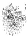
- the shape of the stage apparatus 1301 is such that it is longer in the Y direction, and the measurement optical system 1312 is disposed on the top surface of the frame 1701 ( Figure 17) in the Y direction.
- the transfer position is disposed topmost possible position in the Figure. With those arrangement, the number of movable parts above the mask 2 and the wafer 3 is reduced, so that the problem of contamination falling is eliminated. Also, the mask conveying apparatus 1311, the orientation flat detecting stage 1305, the injector 1304, the wafer traverser 1305 or the like are necessarily disposed at a lower side in the Figure of the transfer position, and therefore, the transfer position is protected from the dust produced by those subunits.
- the vacuum chamber 1408 and the frame 1407 are independently fixed to an unshown base, and therefore, the deformation of the vacuum chamber 1408 attributable to the changes in the temperature for the ambient pressure does not influence the pose or position of the X-ray mirror 1401. Therefore, the rigidity of the vacuum chamber 1408 can be decreased to permit reduction of the weight.
- a discharge port 1411 is connected with a discharge pump 1412 for maintaining a high vacuum in the vacuum chamber 1408.
- a shutter 1409 is provided to avoid that the X-ray mirror 1401 receives the SOR rays when it is not necessary, by which the time period during which the X-ray mirror 1401 is dozed with the SOR rays. The reduction of the time period is contributable to reduce the damage of the X-ray mirror 1401 by the radiation.
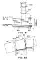
- the steel belt 1517 is stretched between the driving drum 1515 driven by the actuator unit 1518 and the idler drum 1516, and the inside of the steel belt 1515 is driven by the driving drum 1515 through friction.
- the driving drum 1515 is crowned by which the central portion of the drum has a larger diameter than that of the marginal portions by 50 - 100 microns so as to stabilize the movement of the steel belt 1517 without rolling. Adjacent opposite ends of the steel belt 1517, a small rectangular openings are formed, one of which is a timing aperture 1534, and the other of which is a position detecting aperture 1535.
- An X-ray detector is mounted to the fine movement stage 1804 ( Figure 18) when the two shutter units 1501 and 1502 are maintained opened, and a Y coarse movement stage 1705 ( Figure 17) is driven to scanningly move in the Y direction in the exposure area the X-ray detector 1511, the strength profile of the X-ray can be measured.
- a driving table for driving the actuator unit 1514 is produced, and the correcting drive to provide the constant energy absorption of the resist in the exposure area can be effected.
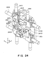
- the actuator units 2415 and 2416 in the ⁇ and ⁇ directions are hermetically sealed by an aluminum alloy casing enclosing a DC motor, a rotary encoder and a reduction mechanism, and similarly to the actuator unit for the exposure shut apparatus 1308, the heat generated by the motor and the reduction mechanism is carried over outside the chamber through an unshown pipes.
- the axis of the pattern on the mask 2 is directly aligned with the movement direction of the reference mark representing the coordinate axis of the stage apparatus 1301 ruling the column and line direction of the patterns, and therefore, the mask alignment is very precise.
- the adjustment is required to mechanically align with high precision the line defined by the two points to the coordinate axis of the stage apparatus 1301.
- such an adjustment is not necessary when the reference marks 1821 which are functionally deemed as one point are mounted on the laser distance measuring mirror 1810. This is particularly advantageous in the easy servicing operation in the field.
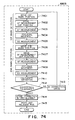
- a mask chamber 3103 is connected through a mask gate valve 3102 which will hereinafter be called also "MKGV".
- the shutter chamber 3104 accommodates the exposure shutter apparatus 1308, and to the chamber 3104 an X-ray mirror port 3105 is conencted through the Be window 3512.
- the prealignment system 1307 is accommodated in the automatic prealignment chamber 3106.
- the mask chamber 3103 contains the mask cassette loader 1309 with the exception of the elevator driving unit 2805 and the indexer.
- a wafer traverser 1304 is accommodated except X, ⁇ y driving units 2516 and 2515.
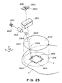
- Figure 40 shows the structures of the fine automatic alignment and automatic focusing controlling sections 3910a - 3910d, in which the elements shown in Figure 23 are omitted.
- a communication path 3909 for communication with the main assembly controlling unit 3902 shown in Figure 39
- a communication interface 3908b for reception of instructions through the communication path 3909 and transmission of alignment information and gap information
- fine alignment and focusing interface 4004 for receiving instructions from the communication interface 3908b, producing signals for alignment measurement and gap measurement and transmitting the alignment information and the gap information to the communication interface 3908b.
- a fine alignment and focusing laser diode driver 4001 drives the semiconductor laser 2301 by the light output determined by the fine alignment and focusing interface 4004.
- the ⁇ axis drivers 4206a - 4206d and ⁇ axis drivers 4207a - 4207d are driver, for DC motors, and it is possible that in response to the instructions from the main control unit 3902, its servo loop is shut off.
- the pickup head cramp controlling section 4205 includes a driver 4208 for an actuator for pressing the pickup device 2401 to the pickup reference surfaces 2401 in order to reduce the position control error by pitching and rolling of the pickup device 2401, and a sensor 4209 for confirming the pressing.
- only one electromagnetic valve (not shown) for a compressed air operable to press the pickups 2401 is provided for four pickup stages 2411.
- the sensor (not shown) for confirmation of the pressed state is provided for each of the pickup stages, and therefore the sensor 4209 is provided with four channel inputs.
- the pressure gauge input portion 4805 receives the sensor output from the mirror port pressure gauge 3519 for measuring the pressure of the mirror port 3105 and a sensor output from the main chamber pressure gauge 3510 for measuring the pressure of the main chamber 3101, and it processes the outputs and transmits the data to the supply and discharge interface 4803.
- the vacuum pump driver 4806 is used commonly for the main chamber 3101, the wafer loading sub-chamber 3109, the wafer unloading sub-chamber 3111 and the mask sub-chamber 3103. It also on-off controls the coarse discharge oil rotation pump 3303 and the main discharge oil rotation pump 3307 and drives and monitors the state of operation of the main discharge turbo molecule pump 3306.
- the mask cassette taking out instructions are to execute the process for taking the mask cassette set into the apparatus by the operator to establish an exchangeable conditions.
- the discrimination is made at step 4917 as to whether or not a mask cassette is currently set, and whether or not the conditions for execution of the mask cassette taking out processing are satisfied. If so, at step 4918 the mask cassette taking out process is executed. Then, the mask cassette 1310 can be taken out, and the sequence goes back to the step 4913.
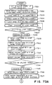
- the X-ray strength profile measurement instructions (step 4922) is to execute the process for producing shutter driving data for assuring uniform X-ray exposure amount over the entire exposure area against change in the X-ray strength profile due to electron injection into the SOR ring 4, exchange of the Be window 3512, X-ray mirror 1401 adjustment or the like. If it is discriminated at step 4922 that the X- ray strength profile measurement instructions are produced, the sequence goes to step 4922 where the discrimination is made as to whether the conditions for execution of the X-ray strength profile measurement are satisfied. If so, the X-ray strength profile measurement process is executed at step 4924 with the use of the X-ray detector 1551 ( Figure 15), and then the sequence goes back to the step 4903.
- the shutter driving data table determined at the step 6207 is set in the source table memory 4308 in the shutter controlling section 3913. This is the end of the X-ray strength profile measurement process.
- Figure 65 illustrates the process for obtaining the shutter driving data from the X-ray strength profile, wherein reference numeral 6501 designates an exposure period curve which is determined from the above described X-ray strength profile 6402 so that the reference X-ray exposure amount separately determined can be provided on the exposure area surface in its entirety.
- the curve 6501 indicates the exposure period until each point in the exposure area is exposed to a reference amount of exposure when the X-ray having the reference X-ray strength DXB is applied to the X-ray illuminometer 1541.
- the speed in the constant speed region is determined on the basis of the minimum exposure period t MIN in the exposure period curve 6501 and the distance l from the leading edge 1531 to the trailing edge 1532 of the shutter; and the exposure period region from the position P MIN providing the minimum exposure period to the shutter movement starting side a difference ⁇ ta at each point is corrected by the leading edge 1531 of the shutter, whereas the period region from the position P MIN to the end side of the shutter, the different ⁇ tb at each point is corrected by the trailing edge 1532; more particularly those corrections are provided by the movement speed of the leading and trailing edges 1531 and 1532 of the shutter by determining the starting curve during the transient period before the constant speed region and the ending curve during the transient region after the constant speed period.
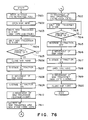
- Step 6817 expresses the synchronization between the concurrent exposure process and wafer collection-supply process.
- the exposed wafer (the wafer on the wafer chuck 1807) and the non-exposed wafer (the wafer on the orientation flat detection chuck 2521) are conveyed to the orientational flat detection chuck 2521 by the unloading hand 2531 and to the wafer chuck 1807 by the loading hand 2530, respectively, at step 6803.
- the sequence goes back to the step 6804 where the exposure process and the wafer collection/supply process are performed concurrently if the earlier wafer supply discrimination at step 6814 is affirmative.
- (x c , y c ) is coordinates of the point of intersection between the line 7201 and the perpendicular line. Since the angle ⁇ OF is determined by tan ⁇ 1, and therefore -90 degrees ⁇ ⁇ OF ⁇ 90 degrees. Therefore, the correction should be made to provide 0 degree ⁇ ⁇ OF ⁇ 360 degrees from the coordinates (x c , y c ).
- the output of the camera sensor 2117 show in Figure 21 is processed by the automatic prealignment and prefocusing controlling section 3910 to determine the deviations of ⁇ X1 and ⁇ Y1 between the target position 7503 and the actual position 7505 of the first mark.
- the thickness deviation ⁇ Z1 from an ideal wafer at the first mark position and the deviations ⁇ X1 and ⁇ Y1 of the first mark from the target position.
- a rotational deviation ⁇ 1 of the wafer 3 is calculated out of the deviations of the two marks.
- "i" in the form of subscript represents number of iteration of the correcting movement loop.
- the calculated ⁇ i is compared with a predetermined tolerable rotational deviation, and if it is outside the tolerance, the ⁇ coarse stage 1806 is actuated by the ⁇ coarse mechanisms 1814 - 1816 shown in Figure 18 to correct only the rotational deviation ⁇ i at step 7413, and the sequence goes to the step 7401 to repeat the operation from the detection of the first mark deviation, at step 7413.
- the correction drive amounts ⁇ Z, ⁇ w, ⁇ y are calculated from the above four point gaps so that the deviation Zexp of the alignment measurement shot exposure gap position is smallest as the entire shot area which is going to be exposed, and in accordance with which the stage controller section 3918 moves the Z tilt stage 1805. With this stage, the automatic focus is completed, so that the gap between the mask 2 and the wafer 3 are substantially uniform.
- the vibration of the main assembly of the exposure apparatus is suppressed by being supported by three air suspensions 8402, 8403 and 8404 disposed on the vibration suppressing frame 8401 fixed on the floor.
- the three air suspensions 8402 and 8404 are connected with three air lines 2412.
Landscapes
- General Physics & Mathematics (AREA)
- Physics & Mathematics (AREA)
- Engineering & Computer Science (AREA)
- Health & Medical Sciences (AREA)
- Public Health (AREA)
- Environmental & Geological Engineering (AREA)
- Epidemiology (AREA)
- Toxicology (AREA)
- Atmospheric Sciences (AREA)
- Life Sciences & Earth Sciences (AREA)
- Multimedia (AREA)
- Exposure And Positioning Against Photoresist Photosensitive Materials (AREA)
- Exposure Of Semiconductors, Excluding Electron Or Ion Beam Exposure (AREA)
Priority Applications (2)
| Application Number | Priority Date | Filing Date | Title |
|---|---|---|---|
| DE68921341T DE68921341T2 (de) | 1989-10-30 | 1989-10-30 | Ausrichtevorrichtung und eine damit versehene Synchrotron-Röntgenbelichtungsvorrichtung. |
| EP89311195A EP0425739B1 (fr) | 1989-10-30 | 1989-10-30 | Dispositif d'alignement et dispositif d'exposition par rayonnement synchrotron dans la gamme des rayons X utilisant celui-ci |
Applications Claiming Priority (1)
| Application Number | Priority Date | Filing Date | Title |
|---|---|---|---|
| EP89311195A EP0425739B1 (fr) | 1989-10-30 | 1989-10-30 | Dispositif d'alignement et dispositif d'exposition par rayonnement synchrotron dans la gamme des rayons X utilisant celui-ci |
Publications (2)
| Publication Number | Publication Date |
|---|---|
| EP0425739A1 true EP0425739A1 (fr) | 1991-05-08 |
| EP0425739B1 EP0425739B1 (fr) | 1995-02-22 |
Family
ID=8202834
Family Applications (1)
| Application Number | Title | Priority Date | Filing Date |
|---|---|---|---|
| EP89311195A Expired - Lifetime EP0425739B1 (fr) | 1989-10-30 | 1989-10-30 | Dispositif d'alignement et dispositif d'exposition par rayonnement synchrotron dans la gamme des rayons X utilisant celui-ci |
Country Status (2)
| Country | Link |
|---|---|
| EP (1) | EP0425739B1 (fr) |
| DE (1) | DE68921341T2 (fr) |
Cited By (3)
| Publication number | Priority date | Publication date | Assignee | Title |
|---|---|---|---|---|
| EP0789280A3 (fr) * | 1996-02-06 | 1998-03-25 | Canon Kabushiki Kaisha | Mécanisme de retenue et appareil d'exposition utilisant le mécanisme |
| EP0856872A3 (fr) * | 1997-01-27 | 2000-12-13 | Nikon Corporation | Appareil d'exposition par faisceau de particules chargées |
| CN117130186A (zh) * | 2023-10-25 | 2023-11-28 | 深圳市晶鸿电子有限公司 | 一种lcd显示屏瑕疵缺陷智能检测方法 |
Citations (2)
| Publication number | Priority date | Publication date | Assignee | Title |
|---|---|---|---|---|
| EP0109193A2 (fr) * | 1982-10-15 | 1984-05-23 | Hitachi, Ltd. | Système lithographique aux rayons X |
| EP0357425A2 (fr) * | 1988-09-02 | 1990-03-07 | Canon Kabushiki Kaisha | Dispositif d'exposition |
-
1989
- 1989-10-30 DE DE68921341T patent/DE68921341T2/de not_active Expired - Fee Related
- 1989-10-30 EP EP89311195A patent/EP0425739B1/fr not_active Expired - Lifetime
Patent Citations (2)
| Publication number | Priority date | Publication date | Assignee | Title |
|---|---|---|---|---|
| EP0109193A2 (fr) * | 1982-10-15 | 1984-05-23 | Hitachi, Ltd. | Système lithographique aux rayons X |
| EP0357425A2 (fr) * | 1988-09-02 | 1990-03-07 | Canon Kabushiki Kaisha | Dispositif d'exposition |
Non-Patent Citations (3)
| Title |
|---|
| JOURNAL OF VACUUM SCIENCE & TECHNOLOGY: PART B vol.1, no.4, October-December 1983, NEW YORK US pages 1262 - 1266; R.P.Haelbich et al.: "Design and performance of an x-ray lithography beam line at a storage ring" * |
| JOURNAL OF VACUUM SCIENCE & TECHNOLOGY: PART B vol.3, no.6, November/December 1985, NEW YORK US pages 1581 - 1586; T.Hayasaka et al.: "A step-and-repeat x-ray exposure system for 0.5 micron pattern replication" * |
| PATENT ABSTRACTS OF JAPAN vol. 9, no. 118 (E-316)(1841) 23 May 1985, & JP-A-60 7722 (FUJITSU K.K.) 16 January 1985, * |
Cited By (5)
| Publication number | Priority date | Publication date | Assignee | Title |
|---|---|---|---|---|
| EP0789280A3 (fr) * | 1996-02-06 | 1998-03-25 | Canon Kabushiki Kaisha | Mécanisme de retenue et appareil d'exposition utilisant le mécanisme |
| US6005910A (en) * | 1996-02-06 | 1999-12-21 | Canon Kabushiki Kaisha | Holding mechanism, and exposure apparatus using the mechanism |
| EP0856872A3 (fr) * | 1997-01-27 | 2000-12-13 | Nikon Corporation | Appareil d'exposition par faisceau de particules chargées |
| CN117130186A (zh) * | 2023-10-25 | 2023-11-28 | 深圳市晶鸿电子有限公司 | 一种lcd显示屏瑕疵缺陷智能检测方法 |
| CN117130186B (zh) * | 2023-10-25 | 2024-01-05 | 深圳市晶鸿电子有限公司 | 一种lcd显示屏瑕疵缺陷智能检测方法 |
Also Published As
| Publication number | Publication date |
|---|---|
| EP0425739B1 (fr) | 1995-02-22 |
| DE68921341D1 (de) | 1995-03-30 |
| DE68921341T2 (de) | 1995-08-17 |
Similar Documents
| Publication | Publication Date | Title |
|---|---|---|
| US5524131A (en) | Alignment apparatus and SOR x-ray exposure apparatus having same | |
| US7126689B2 (en) | Exposure method, exposure apparatus, and method for producing device | |
| JP3747566B2 (ja) | 液浸型露光装置 | |
| EP1650604B1 (fr) | Arrangement de support et méthode de support et de conditionnement thermique d'un substrat | |
| US6864955B2 (en) | Stage apparatus, exposure apparatus and method for exposing substrate plate | |
| US5448612A (en) | X-ray exposure apparatus | |
| US20010055117A1 (en) | Alignment method, exposure method, exposure apparatus and device manufacturing method | |
| US20040227925A1 (en) | Exposure apparatus | |
| KR20100015494A (ko) | 노광 장치 및 디바이스의 제조 방법 | |
| US7315347B2 (en) | Exposure apparatus and device manufacturing method | |
| US20020075467A1 (en) | Exposure apparatus and method | |
| TWI289736B (en) | Lithographic apparatus and device manufacturing method | |
| US20110171759A1 (en) | Lithographic Apparatus and Device Manufacturing Method | |
| US5959304A (en) | Semiconductor exposure apparatus | |
| US7126664B2 (en) | Lithographic apparatus and a device manufacturing method | |
| EP0425739B1 (fr) | Dispositif d'alignement et dispositif d'exposition par rayonnement synchrotron dans la gamme des rayons X utilisant celui-ci | |
| US20060077364A1 (en) | Lithographic apparatus and device manufacturing method | |
| US7349071B2 (en) | Pre-aligning a substrate in a lithographic apparatus, device manufacturing method, and device manufactured by the manufacturing method | |
| JP4838834B2 (ja) | サーボ制御システム、リソグラフィ装置および制御方法 | |
| US20070228295A1 (en) | Lithographic Apparatus, Support, Device Manufacturing Method, and a Method of Supporting | |
| JP6587138B2 (ja) | 物体支持装置及び露光装置 | |
| JP6822534B2 (ja) | 物体支持装置及び露光装置 | |
| JP4048205B2 (ja) | リトグラフ装置及びデバイス製造方法 | |
| US7384228B2 (en) | Insertion device, lithographic apparatus with said insertion device and device manufacturing method | |
| WO2002075795A1 (fr) | Procede et dispositif d'exposition et procede pour produire ledit dispositif |
Legal Events
| Date | Code | Title | Description |
|---|---|---|---|
| PUAI | Public reference made under article 153(3) epc to a published international application that has entered the european phase |
Free format text: ORIGINAL CODE: 0009012 |
|
| 17P | Request for examination filed |
Effective date: 19901231 |
|
| AK | Designated contracting states |
Kind code of ref document: A1 Designated state(s): DE FR GB NL |
|
| 17Q | First examination report despatched |
Effective date: 19930906 |
|
| GRAA | (expected) grant |
Free format text: ORIGINAL CODE: 0009210 |
|
| AK | Designated contracting states |
Kind code of ref document: B1 Designated state(s): DE FR GB NL |
|
| REF | Corresponds to: |
Ref document number: 68921341 Country of ref document: DE Date of ref document: 19950330 |
|
| ET | Fr: translation filed | ||
| PLBE | No opposition filed within time limit |
Free format text: ORIGINAL CODE: 0009261 |
|
| STAA | Information on the status of an ep patent application or granted ep patent |
Free format text: STATUS: NO OPPOSITION FILED WITHIN TIME LIMIT |
|
| 26N | No opposition filed | ||
| REG | Reference to a national code |
Ref country code: GB Ref legal event code: IF02 |
|
| PGFP | Annual fee paid to national office [announced via postgrant information from national office to epo] |
Ref country code: NL Payment date: 20061017 Year of fee payment: 18 |
|
| PGFP | Annual fee paid to national office [announced via postgrant information from national office to epo] |
Ref country code: GB Payment date: 20061018 Year of fee payment: 18 |
|
| PGFP | Annual fee paid to national office [announced via postgrant information from national office to epo] |
Ref country code: DE Payment date: 20061220 Year of fee payment: 18 |
|
| GBPC | Gb: european patent ceased through non-payment of renewal fee |
Effective date: 20071030 |
|
| NLV4 | Nl: lapsed or anulled due to non-payment of the annual fee |
Effective date: 20080501 |
|
| PG25 | Lapsed in a contracting state [announced via postgrant information from national office to epo] |
Ref country code: DE Free format text: LAPSE BECAUSE OF NON-PAYMENT OF DUE FEES Effective date: 20080501 |
|
| REG | Reference to a national code |
Ref country code: FR Ref legal event code: ST Effective date: 20080630 |
|
| PG25 | Lapsed in a contracting state [announced via postgrant information from national office to epo] |
Ref country code: NL Free format text: LAPSE BECAUSE OF NON-PAYMENT OF DUE FEES Effective date: 20080501 |
|
| PGFP | Annual fee paid to national office [announced via postgrant information from national office to epo] |
Ref country code: FR Payment date: 20061019 Year of fee payment: 18 |
|
| PG25 | Lapsed in a contracting state [announced via postgrant information from national office to epo] |
Ref country code: GB Free format text: LAPSE BECAUSE OF NON-PAYMENT OF DUE FEES Effective date: 20071030 |
|
| PG25 | Lapsed in a contracting state [announced via postgrant information from national office to epo] |
Ref country code: FR Free format text: LAPSE BECAUSE OF NON-PAYMENT OF DUE FEES Effective date: 20071031 |