EP0425990A2 - Appareil d'échange de cellules - Google Patents
Appareil d'échange de cellules Download PDFInfo
- Publication number
- EP0425990A2 EP0425990A2 EP90120334A EP90120334A EP0425990A2 EP 0425990 A2 EP0425990 A2 EP 0425990A2 EP 90120334 A EP90120334 A EP 90120334A EP 90120334 A EP90120334 A EP 90120334A EP 0425990 A2 EP0425990 A2 EP 0425990A2
- Authority
- EP
- European Patent Office
- Prior art keywords
- cells
- lines
- buffer
- outgoing
- incoming
- Prior art date
- Legal status (The legal status is an assumption and is not a legal conclusion. Google has not performed a legal analysis and makes no representation as to the accuracy of the status listed.)
- Granted
Links
Images


Classifications
-
- G—PHYSICS
- G06—COMPUTING OR CALCULATING; COUNTING
- G06F—ELECTRIC DIGITAL DATA PROCESSING
- G06F5/00—Methods or arrangements for data conversion without changing the order or content of the data handled
- G06F5/06—Methods or arrangements for data conversion without changing the order or content of the data handled for changing the speed of data flow, i.e. speed regularising or timing, e.g. delay lines, FIFO buffers; over- or underrun control therefor
- G06F5/065—Partitioned buffers, e.g. allowing multiple independent queues, bidirectional FIFO's
-
- H—ELECTRICITY
- H04—ELECTRIC COMMUNICATION TECHNIQUE
- H04L—TRANSMISSION OF DIGITAL INFORMATION, e.g. TELEGRAPHIC COMMUNICATION
- H04L12/00—Data switching networks
- H04L12/54—Store-and-forward switching systems
- H04L12/56—Packet switching systems
- H04L12/5601—Transfer mode dependent, e.g. ATM
-
- H—ELECTRICITY
- H04—ELECTRIC COMMUNICATION TECHNIQUE
- H04L—TRANSMISSION OF DIGITAL INFORMATION, e.g. TELEGRAPHIC COMMUNICATION
- H04L49/00—Packet switching elements
- H04L49/10—Packet switching elements characterised by the switching fabric construction
- H04L49/104—Asynchronous transfer mode [ATM] switching fabrics
- H04L49/105—ATM switching elements
- H04L49/108—ATM switching elements using shared central buffer
-
- H—ELECTRICITY
- H04—ELECTRIC COMMUNICATION TECHNIQUE
- H04L—TRANSMISSION OF DIGITAL INFORMATION, e.g. TELEGRAPHIC COMMUNICATION
- H04L49/00—Packet switching elements
- H04L49/25—Routing or path finding in a switch fabric
- H04L49/253—Routing or path finding in a switch fabric using establishment or release of connections between ports
- H04L49/255—Control mechanisms for ATM switching fabrics
-
- G—PHYSICS
- G06—COMPUTING OR CALCULATING; COUNTING
- G06F—ELECTRIC DIGITAL DATA PROCESSING
- G06F2205/00—Indexing scheme relating to group G06F5/00; Methods or arrangements for data conversion without changing the order or content of the data handled
- G06F2205/06—Indexing scheme relating to groups G06F5/06 - G06F5/16
- G06F2205/066—User-programmable number or size of buffers, i.e. number of separate buffers or their size can be allocated freely
-
- H—ELECTRICITY
- H04—ELECTRIC COMMUNICATION TECHNIQUE
- H04L—TRANSMISSION OF DIGITAL INFORMATION, e.g. TELEGRAPHIC COMMUNICATION
- H04L12/00—Data switching networks
- H04L12/54—Store-and-forward switching systems
- H04L12/56—Packet switching systems
- H04L12/5601—Transfer mode dependent, e.g. ATM
- H04L2012/5678—Traffic aspects, e.g. arbitration, load balancing, smoothing, buffer management
- H04L2012/5681—Buffer or queue management
Definitions
- This invention relates relates to a cell exchanging apparatus for exchanging cells at a high speed which are obtained from various information for multimedia, such as voices, data and images, in blocks.
- Fig. 1 is a block diagram showing a conventional cell exchanging apparatus disclosed in Japanese Patent disclosure No. 117241/90, for example.
- the reference numerals 1 1 - 1 n designate n (n ⁇ 2) incoming lines through which packets are input. Each packet has a fixed length and has a header portion including encoded destination information.
- 2 1 - 2 m designate m (m ⁇ 2) outgoing lines through which the packets are output dependent on the destinations specified by the header portions.
- 3 1 - 3 t designate t (l ⁇ n) buffer memories in which the input packets are temporarily stored.
- 4 designates an empty buffer selection switch for connecting each of the incoming lines 1 1 -1 n , through which a packet is input, to an empty one of the buffer memories 3 1 - 3 l .
- 5 1 - 5 l are header memory circuits provided in correspondence to the buffer memories 3 1 - 3 t for extracting and storing only the header portions of those packets which are stored in the corresponding buffer memories.
- 6 1 - 6 t denote outgoing line selection circuits provided in correspondence to the header memory circuits 5 1 - 5 t for making the outputs thereof significant, i.e., "1", from which the stored contents of the corresponding header memory circuits are sent to output lines.
- 7 1 - 7 m are encoders provided in correspondence to the outgoing lines 2 1 - 2 m for receiving outputs from the outgoing selection circuits 6 1 - 6 L to encode the outputs as buffer numbers of the buffer memories 3 1 - 3 l .
- 8 1 - 8 m are first-in, first-out type (hereinafter referred to FIFO) memories provided in correspondence to the encoders 7 1 - 7 m such that the buffer numbers encoded by the encoders 7 1 - 7 m are written into the FIFO memories and then read out therefrom in the same order that the buffer numbers are input.
- 9 1 - 9 m are buffer connection switches controlled in accordance with the buffer numbers delivered from the corresponding FIFO memories for outputting the packets stored in the buffer memories to the outgoing lines specified by the header portions of the packets.
- both the terms "cell” and “packet” mean the same thing in that multimedia information is divided into blocks and a header including destination information is added to each block. Generally, however, the two terms are different in that the packet is handled as having blocks of variable length, while the cell is handled as having a fixed length prescribed by the International Standard.
- Fig. 2 is a time chart showing a timing relation between signals at the various points. This figure illustrates a flow of control in the case of receiving, at the same time, packets sent from the incoming lines 1 1 and 1 n to the outgoing line 2 1 when the buffer memories 3 1 and 3 t are empty. It is also assumed that the packets handled here have a fixed length as mentioned above and the header portions include, as destination information, encoded outgoing line numbers.
- the empty buffer selection switch 4 selects an empty one of the buffer memories 3 1 - 3 t and connects it to the incoming line along which the packet has arrived.
- the empty buffer selection switch 4 selects the incoming lines 1 1 - 1 n and the buffer memories 3 1 - 3 t one by one in the ascending order, for example, and interconnects a selected pair of the incoming line and the buffer memory.
- the empty buffer selection switch 4 connects the incoming line 1 1 to the buffer memory 3 1 and the incoming line 1 n to the buffer memory 3 t , whereby a packet A having arrived along the incoming line 1, is stored in the buffer memory 3 1 and a packet B having arrived along the incoming line 1 n is stored in the buffer memory 3 t , respectively.
- the packet A is also supplied to the header memory circuit 5 1 corresponding to the buffer memory 3 1 and the packet B is also supplied to the header memory circuit 5 t corresponding to the buffer memory 3 t .
- the header memory circuits 5 1 - 5 t serve to extract only the header portions of the received packets and to store the contents of the header portions, i.e., the outgoing line numbers. Accordingly, the outgoing line number "1" " designating the outgoing line 2 1 is stored in the header memory circuits 5 1 and 5 l .
- the contents of the header memory circuits 5, and 5 l are sent to the corresponding outgoing line selection circuits 6 1 and 6 l , respectively.
- the outgoing line selection circuit 6 1 sets the output to the encoder 7 1 to “1” “ as shown in Fig. 2(c), and the outgoing line selection circuit 6 t also sets the output to the encoder 7 1 to “1” “ as shown in Fig. 2(d).
- a corresponding one of the encoders 7 1 - 7 m encodes the buffer number of the buffer memory which corresponds to one of the outgoing line selection circuits 6 1 - 6 l , and causes the encoded buffer number to be stored in corresponding one of the FIFO memories 8 1 - 8 m .
- the encoder 7 1 causes the buffer numbers to be stored in the FIFO memory 8 1 in the ascending order, for example.
- the FIFO memory 8 1 first stores the buffer number (D of the buffer memory 3 1 and then stores the buffer number of the buffer memory 3 t .
- Each of the buffer connection switches 9 1 - 9 m reads out the buffer numbers, stored in the FIFO memories 8 1 - 8 m , in the order of the buffer numbers stored, and connects the buffer memories designated by the read-out buffer numbers to the outgoing line connected to the buffer connection switch.
- the buffer connection switch 9 first reads the buffer number 1 out of the FIFO memory 8 1 and, after the completion of the necessary connection process, reads the next buffer number therefrom.
- the buffer memory 3i is connected to the outgoing line 2 1 and the packet A stored in the buffer memory 3 1 is output to the outgoing line 2 1 as shown in Fig. 2(f).
- the buffer number is read out as mentioned above, whereupon the buffer memory 3 t is connected to the outgoing line 2 1 and the packet B stored in the buffer memory 3 t is output to the outgoing line 2 1 , as shown in Fig. 2-(g).
- the packets A and B are output to the outgoing line 2i successively as shown in Fig. 2(h).
- the buffer connection switches 9 1 - 9 m resease a corresponding one of the buffer memories 3 1 - 3 t and inform the empty buffer selection switch 4 of the fact so as to make it ready for receiving further packets.
- This invention has been made to solve the problems as explained above, and has for its object to provide a cell exchanging apparatus which can reduce the number of cells discarded due to collisions using a small number of buffer memories, and which can also reduce the size of switching devices for connecting the buffer memories to incoming lines and outgoing lines.
- a cell exchanging apparatus of the present invention comprises header processing circuits provided in correspondence to incoming lines for detecting destinations from header portions of received cells, and a plurality of buffer memories capable of storing the cells in accordance with specified addresses and reading out the stored cells in accordance with the specified addresses independently of the order of the cells stored.
- the header processing circuits are connected to the buffer memories through an incoming line spatial switch, and the buffer memories are connected to the outgoing lines through an outgoing line spatial switch.
- a buffer control circuit controls the incoming line spatial switch to select the buffer memories for writing the cells in the selected buffer memories, and manages the addresses of the written cells in the buffer memories for each of the destinations of the cells.
- the buffer control circuit also controls the outgoing line spatial switch in accordance with those addresses under management so that the cells are output to the specified outgoing lines in a predetermined order.
- the cells input through the incoming lines are stored in the buffer memories selected by the incoming line spatial switch after detection of the cell destinations.
- the addresses of the stored cells in the buffer memories are managed for each of the destinations of the cells.
- the buffer memories are accessed to cause the cells stored therein to be read out and output to the outgoing lines connected to the buffer memories through the outgoing line spatial switch. Consequently, when reading the cells out of the buffer memories, a plurality of cells can be led to the outgoing lines through the spatial switch while avoiding collision between cells.
- a processing speed (rate) is the same throughout the circuits, whereby the cells can be exchanged without any necessity to increase such a speed.
- the number of buffer memories can be reduced, which enables a lowering in the number of cells discarded when the number of written cells exceeds the capacity of the buffer memories, without any necessity to increase the size of the spatial switches for connecting the buffer memories to the incoming lines and the outgoing lines.
- the cells input through the incoming lines are held in the header processing circuits for a period of one time slot.
- the buffer memories are provided in number equal to or greater than (number of incoming lines + number of outgoing lines - 1).
- the buffer control circuit controls the incoming line spatial switch such that the cells held in the header processing circuits are written in the buffer memories which are selected so as to avoid the overlapping of the cells, i.e., to prevent a plurality of cells from being written in one buffer memory at the same time within one time slot.
- the outgoing line spatial switch is controlled such that, when the cells have already been written in the buffer memories and are managed using the addresses in the buffer memories for each of the destinations and for each of the reading time slots so as to avoid the overlapping of the destinations within the same time slot, the cells are output to the outgoing lines specified by the cell header portions in a predetermined order.
- the cells held in the header processing circuits are written in the buffer memories selected so as to avoid the overlapping of the cells within one time slot.
- the cells which are managed using the addresses in the buffer memories for each of the destinations and reading time slots so as to avoid the overlapping of the destinations within the same time slot are read out to the outgoing lines specified by the header portions. Consequently, it is possible to reduce the number of cells discarded due to collision therebetween or delay of the cells during the writing and reading operations.
- outgoing line speed adjusting buffers connected to the buffer memories through the outgoing line spatial switch for storing the cells to adjust an outgoing line speed are additionally provided in correspondence to the outgoing lines.
- the buffer control circuit functions to control the incoming line spatial switch to select the buffer memories in which the cells are to be written, to manage the addresses of the cells written in the buffer memories for each destination, to read the cells out of the buffer memories in accordance with those addresses under management in a predetermined order at a speed r (2 s r ⁇ number of outgoing lines) times the outgoing line speed, to control the outgoing line spatial switch to write the read-out cells in the specified outgoing line speed adjusting buffers in a predetermined order, and to read out those written cells in accordance with the outgoing line speed to output the cells to the outgoing lines.
- the cells the destinations of which have been detected are stored in the selected buffer memories.
- the addresses of the cells stored in the buffer memories are managed for each destination, and the buffer memories are accessed in accordance with those addresses for reading out the stored cells at a speed r (2 r ⁇ number of outgoing lines) times the outgoing line speed. Consequently, when reading the cells out of the buffer memories, a plurality of cells can be led to the outgoing lines through the spatial switch so as to avoid any collision between cells, while allowing the cells up to a number of r to be read out of the same buffer memory in overlapped relation.
- the reading speed is raised as high as r times the outgoing line speed at its maximum and, therefore, the cells can be exchanged without any necessity to increase the speed. Because the opportunities of reading the cells out of the same buffer memory is increased, it is possible to further reduce the number of cells discarded by collision during the reading operation.
- incoming line speed adjusting buffers for storing the cells to adjust an incoming speed are additionally provided in correspondence to the incoming lines.
- the buffer control circuit functions to control the outgoing line spatial switch to control the connection between the buffer memories and the outgoing lines, to control the incoming line spatial switch to select the buffer memories in which the cells are to be written, to write the cells read out of the incoming line speed adjusting buffers to the selected buffer memories at a speed w (2 s w ⁇ number of incoming lines) times the incoming line speed, to manage the addresses of the cells written in the buffer memories for each destination, and to control the outgoing line spatial switch in accordance with those addresses under management to output the cells to the specified outgoing lines in a predetermined order.
- the cells for which destinations have been detected are written in the buffer memories selected by the incoming line spatial switch as a speed w (2 w ⁇ number of incoming lines) times the incoming line speed.
- the addresses of the cells stored in the buffer memories are managed for each destination, and the buffer memories are accessed in accordance with those addresses for reading out the stored cells. Consequently, even in a condition that the buffer memories become almost full with cells and a plurality of cells must be written in one buffer memory in one time slot, it is possible to write up to w cells in one buffer memory.
- a plurality of cells can be led to the outgoing lines through the spatial switch, while avoiding collisions between cells.
- the writing speed is raised as high as w times the incoming line speed at its maximum and, therefore, the cells can be exchanged without any necessity to increase the speed. As a result, it is possible to further reduce the number of cells discarded due to collision during the writing operation.
- Fig. 3 is a block diagram showing the structure of a cell exchanging apparatus according to a first embodiment of the present invention.
- n n (n ? 2) incoming lines through which cells are input, each cell comprising a data portion and a header portion including an outgoing line number as destination information.
- 2 1 - 2 m designates m (m ⁇ 2) outgoing lines through which the cells are output dependent on the designations specified by their header portions.
- the above arrangement is identical to that shown in Fig. 1.
- Denoted by 10a, - 10an are header processing circuits provided in correspondence to the incoming lines 1 1 - 1 n for detecting the outgoing lines designated by the header portions of the cells received through the incoming lines.
- 11, - 11 p designate p (p ⁇ 2) buffer memories, each buffer memory being capable of storing cells at specified addresses and reading out the stored cells by specifying the addresses regardless of the order in which the cells are stored or written.
- These buffer memories 11, - 11 p are different from the conventional buffer memories 3 1 - 3 t shown in Fig. 1 in that a plurality of cells can be stored in each buffer memory.
- each storage control circuit designate storage control circuits provided in correspondence to the buffer memories 11 1 - 11 p , each storage control circuit supervising empty addresses using, for example, an FIFO-type memory to give an associated one of the buffer memories 11 1 - 11 READ and WRITE addresses.
- Denoted by 13 is an incoming line spatial switch for selectively connecting the header processing circuits 10a, - 10an to predetermined buffer memories 11, - 11 p , and 14 designates an outgoing line spatial switch for selectively connecting the buffer memories 11 1 - 11 p to predetermined outgoing lines 2 1 - 2 m .
- Denoted by 15a is a buffer control circuit which functions to (i) control a switching operation of the incoming line spatial switch 13 to select the buffer memories in which cells are to be stored, (ii) manage the addresses of the stored cells in the buffer memories on the basis of the respective destinations of the cells, and (iii) control a switching operation of the outgoing line spatial switch 14 in accordance with the addresses under management for the respective destinations, thereby outputting the cells, in a predetermined order, to the outgoing lines specified by the cell headers.
- the buffer control circuit 15a comprises a first buffer selection circuit 16 which, when a cell arrives along one of the incoming lines 1 1 - 1n, receives the outgoing line number of the cell detected by the header processing circuits 10a, - 10an associated with that incoming line, selects one of the buffer memories 11 1 - 11 p in which the cell is to be stored, and controls a switching operation of the incoming line spatial switch 13 so that the selected buffer memory is connected to the cell-detecting header processing circuit.
- the 17 designates an address exchanging circuit which functions to sort out the arriving cells on the basis of the destinations, i.e., the outgoing lines, by referring to the outgoing line numbers detected by the buffer selection circuit 16, and obtain, from the storage control circuits associated with the buffer memories, the WRITE addresses in the buffer memories in which the cells are written to write the obtained WRITE addresses in address queues (described later).
- Denoted by 18 1 - 18 m are address queues each constituted by an FIFO-type memory and provided in corresponding to the outgoing lines 2 1 - 2 m .
- the address exchanging circuit 17 writes, in the address queues, the WRITE addresses in the buffer memories in which the cells destined for the outgoing lines are stored, in the order in which the addresses arrive, for every outgoing lines 2 i - 2 m corresponding to the address queues.
- 19 designates a second buffer selection circuit which functions to determine the cells to be read out of the buffer memories by referring to the address queues 18 1 - 18 m , send the address read out of the address queues, as READ addresses, to the storage control circuits associated with the corresponding buffer memories, and control a switching operation of the outgoing line spatial switch 14 to cause the buffer memories to the corresponding outgoing lines.
- Fig. 4 is a time chart showing a timing relation between signals at various points in the cell exchanging apparatus.
- the time chart illustrates a control flow in which the number n of the incoming lines 1 1 - 1 n and the number m of the outgoing lines 2 1 - 2 m are respectively four (4) and the number p of the buffer memories 11 1 - 11 p is ten (10). It is also assumed that the cells handled here are input at random and have a fixed length, and that the phases of the respective cells are adjusted prior to being input to the incoming lines 1, - 1 n in such a manner that the cells are supplied at the same phase through all the incoming lines.
- Figs. 4(a) - 4(d) show examples of the cells input to the incoming lines 1 1 - 1 4
- Figs. 4(e) - 4(n) show examples of the cells stored in the buffer memories 11 1 - 11 10 in that case
- the Figs. 4(o) - 4(r) show examples of the cells output to the outgoing lines 2 1 - 2 4 .. It is assumed that all the circuits are synchronized with each other, and one cell per one time slot can be input and output.
- the header processing circuits 10a 1 - 10a 4 When the cells are input to the incoming lines, the header processing circuits 10a 1 - 10a 4 provided in correspondence to the incoming lines 1 1 -1 4 detect the outgoing line numbers from the header portions of the input cells. While referring to the header processing circuits 10a 1 -10a 4 , the first buffer selection circuit 16 of the buffer control circuit 15a instructs the incoming line spatial switch 13 to respectively connect the incoming lines along which the cells have arrived to the buffer memories which are selected for storing the cells.
- the manner in which the incoming line spatial switch 13 connects between the incoming lines and the buffer memories can be described in various ways. It is undesirable that two or more cells to be read exist in the same buffer memory at the time the cells are stored and then read out of the buffer memories. To avoid this, the cells are preferably distributed to a number of buffer memories. To accomplish this the same number of buffer memories as that of the incoming lines is not sufficient. Control is facilitated by using as many buffer memories as possible. As a simpler example of control, it can also be envisaged to select a buffer memory which holds the least number of cells therein, and to write cells in the buffer memory. In other words, when x cells arrive simultaneously, x buffer memories which hold the least number of cells therein are selected, and the incoming lines receiving the x cells are spatially connected to the selected buffer memories.
- Fig. 4 shows, as a further simpler example of control, a manner in which the buffer memories 11 1 - 1110 are sequentially selected and arriving cells are written in the buffer memories.
- the buffer memories 11 1 , 11 2 , 11 3 , ..., 11 10 are written therein successively.
- the first cell of a signal f (referred to as an "F1 cell” herein; the remaining cells are similarly referred to) is input from the incoming line 1 1 , a G1 cell of a signal g from the incoming line 1 2 , and an 11 cell of a signal i from the incoming line 1 4 ..
- the header portion of the respective cells include outgoing line numbers; that is, the F1 cell has the number 0 1 specifying the outgoing line 2 1 , the G1 cell has 0 4 specifying the outgoing line 2 4 , and the 11 cell has O 3 specifying the outgoing line 2 3 , respectively.
- the incoming line spatial switch 13 connects the incoming line 1 1 to the buffer memory 11 1 , the incoming line 1 2 to the buffer memory 11 2 , and the incoming line 1 4 to the buffer memory 11 3 , respectively. Therefore, these cells are stored, in the time slot 2, in the buffer memories 11 1 - 114 at the addresses specified by the storage control circuits 12 1 - 12 3 .
- the storage control circuits 12 1 - 12 3 send the WRITE addresses of the buffer memories to the address exchanging circuit 17.
- the WRITE addresses are selected from among those addresses which are managed by the storage control circuits 12 1 - 12 3 as empty addresses.
- the address exchanging circuit 17 sorts out the input cells for each destination outgoing line in reference to the first buffer selection circuit 16, and writes the WRITE address of the buffer memory 11, in the tail end of the address queue 18 1 , the WRITE address of the buffer memory 11 2 in the tail end of the address queue 18 4 , and the WRITE address of the buffer memory 11 3 in the tail end of the address queue 18 3 , respectively.
- the second buffer selection circuit 19 takes out the addresses stored in the address queues 18 1 - 18 3 , sends the addresses to the storage control circuits 12 1 - 12 3 associated with the buffer memories 11 1 -11 3 , and instructs the outgoing line spatial switch 14 to connect the buffer memories 11 1 - 11 3 to the outgoing lines 2 1 , 2 3 and 2 4 , respectively.
- the outgoing line spatial switch 14 connects the buffer memory 11, to the outgoing line 2 1 , the buffer memory 11 2 to the outgoing line 2 4 and the buffer memory 11 3 to the outgoing line 2 3 , respectively, in the time slot 3.
- the storage control circuits 12i -12 3 send the received addresses to the associated buffer memories 11 1 - 11 3 as READ addresses and, thereafter, manage those addresses as empty ones.
- the cells read out of the respective buffer memories 11, - 11 3 are output to the destination outgong lines 2,, 24 and 2 3 specified by their headers, respectively.
- the cells input in the time slot 2 have the header portions specifying the same destination outgoing lines.
- An F2 cell, a G2 cell and an H1 cell input in the time slot 2 are respectively written in the buffer memories 11 4 , 11 s and 11 6 in a like manner, but the header portions of these three cells include the outgoing line number 04 specifying the same outgoing line 2 4 .
- higher priority is given for an incoming line of a smaller number, thereby to causing cells to be delayed.
- the F2, G2 and H1 cells are read out of the buffer memories 11 4 , 11 5 and 11 6 in this order in time slots 4, 5 and 6, respectively, and output to the outgoing line 2 4 . Subsequently, such cell exchange will be executed in the manner described above.
- an 12 cell and an H6 cell are stored in the buffer memory 11 3 .
- these 12 and H6 cells have different destinations, i.e., the outgoing line 2 2 and the outgoing line 2 3 , respectively, they are stored in the same buffer memory 11 3 and hence cannot be taken out simultaneously.
- a collision of the two cells can be avoided by giving the outgoing lines 2i - 2 4 fixed preferential orders or variable preferential orders to be changed on the basis of a random number and by taking out only one cell, e.g., the 12 cell while delaying the other H6 cell.
- a similar event also occurs in other time slots 9, 10 and 15, but not cell is lost due to collision.
- the cells input through the incoming lines are stored in the respective buffer memories selected by the incoming line spatial switch, after the detection of the cell destinations.
- the addresses of the stored cells in the buffer memories are managed for each of the destinations of the cells.
- the buffer memories are accessed for reading out the cells stored therein and outputting those cells to desired outgoing lines connected to the buffer memories through the outgoing line spatial switch.
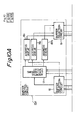
- Fig. 5 is a block diagram showing the construction of a cell exchanging apparatus according to a second embodiment of the present invention.
- the same or corresponding elements are denoted by the same reference numerals as in the cell exchanging apparatus according to the first embodiment and not explained here.
- 10b 1 - 10b n are header processing circuits provided in correspondence to the incoming lines 1 1 - 1 n for detecting the outgoing lines from the header portions of the cells input through the incoming lines and for holding the cells therein for a period of one tme slot.
- 15b designates a buffer control circuit which (i), for a period of one time slot, controls a switching operation of the incoming line spatial switch 13 to select the buffer memories in which the cells are to be written (i.e., the writing of cells), (ii) manages, for each of the destination of the cells and for each time slot for reading out the cells, the addresses of the stored cells in the buffer memories and (iii) outputs the cells in each reading time slot to the outgoing lines specified by their headers in a predetermined order.
- the buffer control circuit 15b comprises an address table 21 provided in correspondence to the outgoing lines 2 1 - 2 m .
- the address table 21 receives the outgoing line numbers of the arriving cells which are detected by the header processing circuits associated with the incoming lines, and selects the buffer memories in which the cells are to be stored, and then stores the buffer memory numbers and the corresponding WRITE addresses in the table for each of the destination outgoing lines.
- 20 designates an incoming line connection instructing circuit which receives the number of the buffer memories storing the cells determined by the address table 21 and the WRITE addresses and controls a switching operation of the incoming line spatial swtich 13 to connect between the header processing circuits 10bi - 10b n and the buffer memories 11 1 - 11 p.
- 22 designates an outgoing line connection instructing circuit which determines the cells to be read out of the buffer memories in reference to the address table 21, sends the addresses read out of the address table 21, as READ addresses, to the storage control circuits associated with the buffer memories, and controls a switching operation of the outgoing line spatial switch 14 to connect the buffer memories to the corresponding outgoing lines respectively.
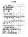
- Fig. 6 is a time chart showing a timing relation between signals at various points in the cell exchanging apparatus.
- the time chart illustrates a control flow in which the number n of the incoming lines 1 1 - 1 n and the number m of the outgoing lines 2 1 - 2 m are each four (4) and the number p of the buffer memories 11 1 - 11 is equal to (n + m - 1); i.e., seven (7).
- the cells handled here have a fixed length, and that the input phases of the respective cells are adjusted prior to being input to the incoming lines 1 1 - 1 n in such a manner that input cells are supplied at the same phase through all the incoming lines.
- those incoming lines 1 1 - 1 4 . are indicated by 1 0 , 1 1 , 1 2 and 1 3
- those outgoing lines 2 1 - 2 4 are indicated by Oo, 0 1 , 0 2 and 0 3 , respectively.
- the buffer memories 11 1 -11 7 are indicated by buffer #0, buffer #1, ..., buffer #6, respectively.
- Fig. 6(a) shows time slot numbers
- Fig. 6(b) shows examples of the cells input to the incoming lines l o - 1 3
- Fig. 6(c) shows the internal state of the address table 21
- Figs. 6(d) and (e) show the internal states of the incoming line connection instructing circuit 20 and the outgoing line connection instruction circuit 22, respectively
- Fig. 6(f) shows the state of the buffer memories 11 1 - 11 7 storing cells
- Fig. 6(g) shows the cells output through the outgoing lines 0 1 - 0 3 . It is assumed that all the circuits are synchronized with each other, and only on cell can be input and output per one time slot.
- the header processing circuits 10bi - 10b 4 When the cells are input to the incoming lines, the header processing circuits 10bi - 10b 4 provided in correspondence to the incoming lines lo - 1 3 detect the outgoing line numbers from the header portions of the input cells, and hold the cells for a period of one time slot.
- the address table 21 in the buffer control circuit 15b determines in which buffer memory the cells input through the incoming lines are to be written.
- the incoming line spatial switch 13 connects the incoming lines at which the cells have arrived to the buffer memories which have been selected for storing the cells. Because only one cell can be written in and read out of one buffer memory within the same one time slot, the buffer memories 11 1 - 117 must be so selected that the writing and reading of a plurality of cells do not occur in the same time slot.
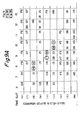
- the address table 21 includes a table rows of which represent destination outgong lines and columns of which represent reading time slots. Each of the boxes in the table contains the buffer memory number and the address in the buffer memory in which the cell to be read out in that time slot is written. Null signals are put in those boxes corresponding to the outgoing lines through which no cells are to be output in any time slots.
- the incoming line spatial switch 13 can be considered to connect the cells to the buffer memories 11 1 - 117 in various ways. It is, however, undesirable for two or more cells to exist in the same one buffer memory in the case where the cells are stored and then read out of the buffer memories. To prevent this situation, the cells are preferably distributed to a number of buffer memories.
- the number p of the buffer memories should be at least (number n of incoming lines) + (number m of outgoing lines) - 1. (In this second embodiment, the number p of the buffer memories is 7.)
- Fig. 6 the matrix-like table in the address table 21 is partitioned for each of the reading time slots. Because the capacity is finite, the table is cyclically reused in various time slots. To this end, a READ pointer rp is employed to point a READ position in the next time slot, and is cyclically updated. The table is arranged to prepare queues for the arriving cells in the order of arrival for each of the destination outgoing lines.
- Fig. 6 shows an example of WRITE pointers wp o - wp 3 employed for the respective destination outgoing lines to point the next writing positions next to the tail ends of the respective queues.
- the buffer memories 11 1 - 11 7 are checked sequentially from the incoming lines 1 1 - l 3 to confirm that the writing of a plurality of cells in the same buffer memory will not be effected in the same time slot and that the reading of a plurality of cells out of the same buffer memory will not be effected in the same time slot, and then buffer memories in which the cells to be written are determined. In this case, those buffer memories which are not filled with cells are selected in a cyclic manner.
- Fig. 6 it is assumed that no cell arrives before a time slot 1, and that three cells arrive through the incoming lines lo, I 1 and 1 3 in the time slot 1. each cell is identified using the incoming line number, the outgoing line number and the time slot in which the cell arrived. For instance, a cell 312 indicates that his cell arrives through the incoming line 1 3 in the time slot 2 and is destined for the outgoing line 0 1 .
- the READ pointer rp is positioned at the column No. 2 in the table in the time slot 1, and, it is assumed that, though not shown in Fig. 6, the WRITE pointer wpo - wp 3 are all positioned at the column No. 3 in the table at the beginning of the time slot 1.
- a cell 011 arriving through the incoming line lo is stored in, for example, the buffer #0 because no other cell exists the table at this time slot.
- This buffer memory 11 1 is associated with the storage control circuit 12 1 for managing the WRITE addresses.
- the WRITE address of the cell 011 is assumed to be 0.
- the upper side represents a buffer memory number and the lower side represents an address in the buffer memory.
- a cell 121 arriving through the incoming line 1, is destined for the outgoing line 0 2 and, therefore, a buffer memory other than the buffer #0, for example, the buffer #1, used for storing the cell 011 is selected as a candidate. In reading the cell 121, it is required to check the column No. 3 in the table.
- the buffer #1 meets the requirements. Accordingly, the cell 121 is stored at an address 0 in the buffer #1. A cell 311 arriving through incoming line 1 3 is destined for the outgoing line 0 1 and, therefore, stored at an address 0 in a buffer other than the buffer #0 and #1 used for storing the cells 011 and 121, that is, in the buffer #2, for example.
- the address table 21 sends constructions to the incoming line connection instructing circuit 20 and the outgoing line connection instruction circuit 22 to cause the incoming line spatial switch 13 and the outgoing line spatial switch 14 to perform necessary exchanging operations.
- the incoming line spatial swtich 13 connects the incoming line lo to the buffer #0, the incoming line 1 1 to the buffer #1 and the incoming line 1 3 to the buffer #2, respectively and the cells are written in these buffers in the time slot 2.
- the column No. 2 of the table pointed by the READ pointer rp is fully occupied by null signals and, therefore, the outgoing line connection instructing circuit 22 is instructed to cause the outgoing line spatial switch 14 to perform no exchanging operation.
- the time slot 2 cells arrive through all the incoming lines 1 0 - 1 3 . Similar to the operation in the time slot 1, some of the buffer memories 11 1 - 11 7 are selected so that a plurality of cells will not be written in or read out of the same buffer memory in the same time slot.
- the READ pointer rp is updated by one as compared with the time slot 1 and positioned in the column No. 3 of the table.
- the cell information in the column No. 3 of the table is sent to the outgoing line connection instructing circuit 22.
- the outgoing line spatial switch 14 then connects the buffer #0 to the outgoing line 0 1 and the buffer #1 to the outgoing line 0 2 in a time slot 3, respectively, and the reading of the cells is effected in the time slot 3.
- the buffer memories 11 1 - 11 7 are checked in turn to confirm that a plurality of cells will not be written in the same buffer memory in the same single time slot, and a plurality of cells will not be read out of the same buffer memory in the same single time slot. Then, a buffer memory in which the cell is to be written is determined as a candidate. At this time, those buffer memories which are not filled with the cells are selected as candidates in a cyclic manner. In a time slot 4, a cell 134 being destined for an outgoing line 0 3 , the buffer #5 was first selected as a candidate. However, because the cell in the buffer #5 is read out in the same time slot, the buffer #6 is determined as a candidate. Likewise, the buffer #3 is finally selected for a cell 304. These two examples are indicated by o in Fig. 6.
- one time slot is set as the unit of an operation cycle, and cells are written in buffer memories selected so as to avoid overlapping of the cells within each time slot.
- Cells are written in buffer memories, and are managed, in addresses in the buffer memories, for each destination and for each reading time slot in such a manner as to avoid overlapping of destinations within the same time slot.
- Those cells are then output to predetermined outgong lines. Consequently, as compared with the case of merely allocating the buffer memories 11 1 -11 7 in a cyclic manner, it is possible to avoid any collision between cells, and hence discarding of cells due to collision and delayed reading of the cells during the writing and reading operations can be avoided.
- Fig. 7 is a block diagram showing the construction of a cell exchanging apparatus according to the third embodiment of the present invention.
- the same or corresponding elements are denoted by the same reference numerals as those in the cell exchanging apparatus according to the first embodiment and are not explained here.
- outgoing line speed adjusting buffers 231 - 23 m are provided in correspondence to the outgoing lines 2 1 - 2 m to be connected to predetermined buffer memories through the outgoing line spatial switch 14.
- the speed adjusting buffers store the cells read out of the buffer memories at a speed r (2 ⁇ r ⁇ number of outgoing lines) times the outgoing line speed, and then output the cells of the corresponding outgong lines in accordance with the outgoing line speed.
- a buffer control circuit 15c comprises a first buffer selection circuit 16, an address exchanging circuit 17, address queues 181 - 18 m and a second buffer selection circuit 19.
- the buffer control circuit 15c functions to (i) control a switching operation of the incoming line spatial switch 13 to select the buffer memories in which cells are to be written, (ii) manage the addresses of the written cells in the buffer memories for each of the destinations of the cells, (iii) cause the cells to be read out of the buffer memories in accordance with the managed addresses in a predetermined order at a speed r (2 ⁇ r ⁇ number of outgoing lines) times the outgoing lines speed, (iv) control the outgoing line spatial switch 14 to cause the read-out cells to be output to the outgoing lines specified by the header portions, (v) write the cells in the corresponding outgoing line speed adjusting buffers, and (vi) read out the stored cells in accordance with the outgoing line speed for outputting them to the corresponding outgoing lines.
- Fig. 8 is a time chart showing a timing relation between signals at various points in the cell exchanging apparatus. Similar to the first embodiment, the time chart illustrates a control flow in which the number n of the incoming lines 1i - 1 n and the number m of the outgoing lines 2 1 - 2 m are each four (4) and that the number p of the buffer memoires 11 1 - 11 p is ten (10).
- Figs. 8(a) -8(r) show the same states as those in Figs. 4(a) - 4(r), respectively.
- the basic sequence of exchanging cells proceeds in a manner similar to the first embodiment. It is noted that an 12 cell and an H6 cell are both stored in the buffer memory 11 3 in a time slot 8 as illustrated. Although the 12 and H6 cells have destinations different from each other; that is, the 12 cell is destined for the outgoing line 2 2 and the H6 cell is destined for the outgoing cell 2 3 , because these cells are stored in the same buffer memory 11 3 , they cannot be taken out simultaneously at a speed equal to the outgoing line speed in the outgoing lines 2 1 - 2 4 ..
- Fig. 9 is a time chart partially showing the time slots 6 - 13 in Fig. 8 on a larger scale.
- Fig. 9 shows the case where the cells are read out of the buffer memories 11 1 - 11 10 at a speed 3 times the outgoing line speed in the outgoing lines 2 1 - 2 m .
- Figs. 9(e) - 9(n) show examples of the cells stored in the buffer memories 11 1 - 11 10
- Figs. 9(s) - 9(v) show states of the cells written in the outgoing line speed adjusting buffers 23 1 - 23 4
- Figs. 9(o) - 9(r) show examples of the cells output to the outgoing lines 2 1 - 2 4 , respectively.
- the 12 cell and the H6 cell in the buffer memory 11 3 are destined for different destinations in the same time slot 8.
- both the 12 and H6 cells would be simultaneously output to the corresponding outgoing lines 2 2 and 2 3 by reading these cells out of the buffer memory 11 3 at a speed 3 times the outgoing lines speed.
- the speed of reading cells out of the buffer memories 11 1 - 11 10 is not limited to 3 times the outgoing line speed, and may be generally set at r (2 5 r ⁇ number of outgoing lines) times the outgoing line speed. While it is assumed that the buffer memories 11 1 - 11 10 are of the type of a dual-port memory, this embodiment is also made feasible by using single-port memories which can operate at a speed double or more the outgoing line speed.
- Fig. 10 is a block diagram showing the construction of a cell exchanging apparatus according to a fourth embodiment of the present invention.
- the same or corresponding elements are denoted by the same reference numerals as those in the cell exchanging apparatus according to the third embodiment and are therefore not explained here.
- incoming line speed adjusting buffers 24 1 - 24 n are provided in correspondence to the incoming lines 1 1 - 1 for storing the cells output from the corresponding header processing circuits 10a 1 - 10an and for then reading the stored cells at a speed w (2 ⁇ w ⁇ number of incoming lines) times the incoming line speed to deliver the cells to predetermined buffer memories 11 1 - 11 through the incoming line spatial switch 13.
- a buffer control circuit 15d comprises a first buffer selection circuit 16, an address exchanging circuit 17, address queues 18 i - 18 m and a second buffer selection circuit 19.
- the buffer control circuit 15d functions to (i) cause the cells stored in the incoming line speed adjusting buffers to be read out at a speed w (2 w ⁇ number of incoming lines) times the incoming line speed, (ii) control the incoming line spatial switch 13 to select the buffer memories in which the cells are to be written, (iii) cause the read-out cells to be written the selected buffer memories at a speed w times the incoming line speed, (iv) manage the addresses of the cells written in the buffer memories for each of the destinations of the cells, and (v) control the outgoing line spatial switch 14 in accordance with those addresses under management for outputting the cells in a predetermined order to the outgoing lines specified by the header portions.
- Fig. 11 is a time chart showing a timing relation between signals at various points in the cell exchanging apparatus of Fig. 10. Similar to the first embodiment shown in Fig. 4, the time chart illustrates a control flow in which the number n of the incoming lines 1 i - 1 n and the number m of the outgoing lines 2 1 - 2 m are each four (4) and that the number p of the buffer memories 11 1 -11 p is ten (10).
- Figs. 11 (a) - 11 (r) show the same states as those in Figs. 4(a) - 4(r), respectively.
- the buffer memories 11 1 - 11 p each have capacities equal to two cells, that cells handled in this embodiment are input at random and have a fixed length, and that the phases of respective cells input are adjusted prior to being input to the incoming lines 1 1 - 1 n in such a manner that the input cells are supplied at the same phase through all the incoming lines.
- the header processing circuits associated with the incoming lines detect outgoing line numbers from the cell headers and cause the cells to write in the corresponding incoming line speed adjusting buffers.
- the first buffer selection circuit 16 in the buffer control circuit 15d instructs the incoming line spatial switch 13 to interconnect the incoming line speed adjusting buffers in which the cells have been written and the buffer memories selected for storing the cells, respectively.
- a speed of reading cells out of the incoming line speed adjusting buffers 24 1 - 24 4 i.e., a speed of writing cells in the buffer memories 11 1 - 11 1 o is assumed to be set 2 times the incoming line speed in the incoming lines 1, -1 4 , thereby allowing two cells to be written in the same buffer memory in one time slot.
- the buffer memories 11 1 , 11 2 , 11 3 , ..., 11 10 are selected in this order to cause the arriving cells to be written in the buffer memories in the order of arrival, if some of the buffer memories in which cells are to be written in any time slot are already filled with the cells, the filled buffer memoires are skipped over, and a cell is written in the next buffer memory.
- the cells are preferably distributed by being written in the buffer memories.
- the speed of writing cells in the buffer memories 11 1 - 11 10 is set at 2 times the incoming line speed, it is possible to write a plurality (two) of cells in which of the buffer memoires 11 1 - 11 10 in one time slot if any cells are unavoidably discarded, thereby reducing the number of cells discarded.
- Fig. 11 because the buffer memory 11 6 is empty to be able to receive two cells and the buffer memory 11 7 is empty to be able to receive one cell in a time slot 11, three cells, i.e., F10, H10 and 18 cells input in the time slot 11 cannot be written in different buffer memories.
- the speed of writing cells in the buffer memories 11 1 - 11 10 is twice the incoming line speed, therefore, the both F10 and H10 cells are written in the buffer memory 11 6 in order to prevent the cells from being discarded.
- the state after those three cells have been written in the buffer memories is indicated in Figs. 11 (i) and 11(j) by putting the symbols F10, H10 and 18 is circles.
- the basic sequence of exchanging cells proceeds in a manner similar to the first embodiment.
- the speed of writing cells in the buffer memories 11 1 - 11 10 is set at 2 times the incoming line speed in the above case, that speed may generally be set to w (2 ⁇ w ⁇ number of incoming lines) times the incoming line speed. While it is assumed that the buffer memories 11 1 - 11 10 are each constituted by dual-port memories, this embodiment is also made feasible by using single-port memories which can operate at a double speed or more.
- destinations of cells are detected and the cells are then written, at a speed w (2 s w ⁇ number of incoming lines) times the incoming line speed, in the buffer memories selected by the incoming line spatial switch. It is therefore possible to write no more than w cells in the same buffer memory and hence to reduce the number of cells discarded due to collision during the writing operation.
Landscapes
- Engineering & Computer Science (AREA)
- Computer Networks & Wireless Communication (AREA)
- Signal Processing (AREA)
- Theoretical Computer Science (AREA)
- Physics & Mathematics (AREA)
- General Engineering & Computer Science (AREA)
- General Physics & Mathematics (AREA)
- Data Exchanges In Wide-Area Networks (AREA)
Applications Claiming Priority (6)
| Application Number | Priority Date | Filing Date | Title |
|---|---|---|---|
| JP27564589 | 1989-10-23 | ||
| JP275645/89 | 1989-10-23 | ||
| JP51120/90 | 1990-03-02 | ||
| JP5112090 | 1990-03-02 | ||
| JP17899390 | 1990-07-06 | ||
| JP178993/90 | 1990-07-06 |
Publications (3)
| Publication Number | Publication Date |
|---|---|
| EP0425990A2 true EP0425990A2 (fr) | 1991-05-08 |
| EP0425990A3 EP0425990A3 (en) | 1992-09-16 |
| EP0425990B1 EP0425990B1 (fr) | 1998-07-22 |
Family
ID=27294212
Family Applications (1)
| Application Number | Title | Priority Date | Filing Date |
|---|---|---|---|
| EP90120334A Expired - Lifetime EP0425990B1 (fr) | 1989-10-23 | 1990-10-23 | Appareil de commutation de cellules |
Country Status (4)
| Country | Link |
|---|---|
| US (1) | US5649217A (fr) |
| EP (1) | EP0425990B1 (fr) |
| CA (1) | CA2028329C (fr) |
| DE (1) | DE69032498T2 (fr) |
Cited By (2)
| Publication number | Priority date | Publication date | Assignee | Title |
|---|---|---|---|---|
| EP0700187A3 (fr) * | 1994-09-02 | 1999-11-10 | Mitsubishi Denki Kabushiki Kaisha | Procédé et dispositif pour la commutation de cellules |
| EP0969356A3 (fr) * | 1998-06-30 | 2001-02-14 | Sun Microsystems, Inc. | Système et procédé pour la gestion de tampons utilisant des tampons PEPS à pointeurs libre, contentant des pointeurs aux tampons vides |
Families Citing this family (21)
| Publication number | Priority date | Publication date | Assignee | Title |
|---|---|---|---|---|
| US5991835A (en) * | 1994-11-22 | 1999-11-23 | Teac Corporation | Peripheral data storage device in which time interval used for data transfer from relatively fast buffer memory to relatively slower main memory is selected in view of average of time intervals during which data blocks were recently received from host |
| JP3075163B2 (ja) * | 1996-01-10 | 2000-08-07 | 日本電気株式会社 | マルチポートフレーム交換方式 |
| JPH10283088A (ja) * | 1997-04-02 | 1998-10-23 | Oki Electric Ind Co Ltd | シリアル通信回路 |
| US6122274A (en) * | 1997-11-16 | 2000-09-19 | Sanjeev Kumar | ATM switching system with decentralized pipeline control and plural memory modules for very high capacity data switching |
| JPH11261566A (ja) * | 1998-03-09 | 1999-09-24 | Fujitsu Ltd | 画像伝送装置 |
| US6239815B1 (en) | 1998-04-03 | 2001-05-29 | Avid Technology, Inc. | Video data storage and transmission formats and apparatus and methods for processing video data in such formats |
| US6275508B1 (en) * | 1998-04-21 | 2001-08-14 | Nexabit Networks, Llc | Method of and system for processing datagram headers for high speed computer network interfaces at low clock speeds, utilizing scalable algorithms for performing such network header adaptation (SAPNA) |
| EP1180874A4 (fr) * | 1999-05-28 | 2008-02-27 | Fujitsu Ltd | Procedes et dispositifs de lecture et d'ecriture de messages, et logiques d'adressage memoire de lecture et d'ecriture de messages de longueur variable |
| JP4222694B2 (ja) * | 1999-08-30 | 2009-02-12 | 富士通株式会社 | Atmセル多重装置 |
| US6477595B1 (en) * | 1999-10-25 | 2002-11-05 | E-Cell Technologies | Scalable DSL access multiplexer with high reliability |
| US7102999B1 (en) * | 1999-11-24 | 2006-09-05 | Juniper Networks, Inc. | Switching device |
| US6704817B1 (en) * | 2000-08-31 | 2004-03-09 | Hewlett-Packard Development Company, L.P. | Computer architecture and system for efficient management of bi-directional bus |
| US7006505B1 (en) * | 2000-10-23 | 2006-02-28 | Bay Microsystems, Inc. | Memory management system and algorithm for network processor architecture |
| JP4185678B2 (ja) * | 2001-06-08 | 2008-11-26 | 株式会社日立製作所 | 液晶表示装置 |
| US7145567B2 (en) | 2003-04-03 | 2006-12-05 | Avid Technology, Inc. | Bitstream format and reading and writing methods and apparatus therefor |
| WO2006026461A2 (fr) * | 2004-08-27 | 2006-03-09 | Board Of Regents, The University Of Texas System | Procedes pour systemes d'attribution de memoire et architecture pour commutateurs internet a base de modules de memoire parallele partageable |
| US7639678B2 (en) * | 2004-12-02 | 2009-12-29 | Nortel Networks Limited | Multimodal data switch |
| US9154255B2 (en) | 2009-08-27 | 2015-10-06 | Maged E. Beshai | Single-rotator latent space switch with an external controller |
| US8971340B2 (en) | 2009-08-27 | 2015-03-03 | Maged E. Beshai | Latent space switch using a single transposing rotator |
| US9252909B2 (en) | 2009-08-27 | 2016-02-02 | Maged E. Beshai | Single-rotator latent space switch with an embedded controller |
| FR2982054B1 (fr) * | 2011-10-28 | 2014-06-20 | Ingenico Sa | Procede et dispositif de gestion d'une matrice de touches, produit programme d'ordinateur et moyen de stockage correspondants. |
Family Cites Families (14)
| Publication number | Priority date | Publication date | Assignee | Title |
|---|---|---|---|---|
| US4692894A (en) * | 1984-12-18 | 1987-09-08 | Advanced Micro Devices, Inc. | Overflow/Underflow detection for elastic buffer |
| US4734907A (en) * | 1985-09-06 | 1988-03-29 | Washington University | Broadcast packet switching network |
| US4920534A (en) * | 1986-02-28 | 1990-04-24 | At&T Bell Laboratories | System for controllably eliminating bits from packet information field based on indicator in header and amount of data in packet buffer |
| US4949301A (en) * | 1986-03-06 | 1990-08-14 | Advanced Micro Devices, Inc. | Improved pointer FIFO controller for converting a standard RAM into a simulated dual FIFO by controlling the RAM's address inputs |
| US4851991A (en) * | 1987-02-24 | 1989-07-25 | Digital Equipment Corporation | Central processor unit for digital data processing system including write buffer management mechanism |
| BE1000396A7 (fr) * | 1987-03-18 | 1988-11-22 | Electronique Et Telecomm Bell | Systeme de commutation. |
| FR2618624B1 (fr) * | 1987-07-24 | 1992-04-30 | Michel Servel | Systeme de commutation de multiplex temporels hybrides a memoire tampon optimisee |
| US5144622A (en) * | 1988-02-15 | 1992-09-01 | Hitachi, Ltd. | Network system |
| US4975906A (en) * | 1988-02-15 | 1990-12-04 | Hitachi, Ltd. | Network system |
| JPH0211724A (ja) * | 1988-06-29 | 1990-01-16 | Kawasaki Steel Corp | 鋼管の浸漬焼入れ時における焼割れ防止方法 |
| JP2910770B2 (ja) * | 1989-03-20 | 1999-06-23 | 富士通株式会社 | 自己ルーチング交換システム及び自己ルーチング交換システムの現用/予備切替え方法 |
| JP2795375B2 (ja) * | 1989-03-01 | 1998-09-10 | 富士通株式会社 | Atm交換装置及びその現用/予備切替え方法 |
| US5210744A (en) * | 1989-06-28 | 1993-05-11 | Mitsubishi Denki Kabushiki Kaisha | Cell exchange apparatus |
| JPH03182140A (ja) * | 1989-12-11 | 1991-08-08 | Mitsubishi Electric Corp | 共通バッファ形交換装置 |
-
1990
- 1990-10-23 EP EP90120334A patent/EP0425990B1/fr not_active Expired - Lifetime
- 1990-10-23 DE DE69032498T patent/DE69032498T2/de not_active Expired - Lifetime
- 1990-10-23 CA CA002028329A patent/CA2028329C/fr not_active Expired - Lifetime
-
1993
- 1993-09-02 US US08/116,215 patent/US5649217A/en not_active Expired - Lifetime
Cited By (2)
| Publication number | Priority date | Publication date | Assignee | Title |
|---|---|---|---|---|
| EP0700187A3 (fr) * | 1994-09-02 | 1999-11-10 | Mitsubishi Denki Kabushiki Kaisha | Procédé et dispositif pour la commutation de cellules |
| EP0969356A3 (fr) * | 1998-06-30 | 2001-02-14 | Sun Microsystems, Inc. | Système et procédé pour la gestion de tampons utilisant des tampons PEPS à pointeurs libre, contentant des pointeurs aux tampons vides |
Also Published As
| Publication number | Publication date |
|---|---|
| DE69032498D1 (de) | 1998-08-27 |
| EP0425990A3 (en) | 1992-09-16 |
| CA2028329C (fr) | 2000-01-18 |
| US5649217A (en) | 1997-07-15 |
| EP0425990B1 (fr) | 1998-07-22 |
| CA2028329A1 (fr) | 1991-04-24 |
| DE69032498T2 (de) | 1999-03-04 |
Similar Documents
| Publication | Publication Date | Title |
|---|---|---|
| US5649217A (en) | Switching system having control circuit and plural buffer memories for data exchange in asynchronous transfer mode | |
| US4788679A (en) | Packet switch with variable data transfer rate links | |
| KR100356447B1 (ko) | 메모리인터페이스유닛,공유메모리스위치시스템및관련방법 | |
| EP0299473B1 (fr) | Système de commutation et son procédé de construction | |
| US5099475A (en) | Switching system | |
| EP0195589B1 (fr) | Système de commutation pour la transmission de données | |
| EP0603916A2 (fr) | Système de commutation de paquets utilisant l'état d'occupation des mémoires de sortie | |
| EP0357618B1 (fr) | Systeme de commutation | |
| EP1030483B1 (fr) | Commutateur ATM | |
| JP3269273B2 (ja) | セル交換装置及びセル交換システム | |
| EP0405530B1 (fr) | Dispositif de commutation de cellules | |
| JPH11266272A (ja) | 共用バッファ制御装置 | |
| EP0519563A2 (fr) | Système pour convertir des signaux à multiplexage temporelle synchrones en paquets de données asynchrones | |
| EP0417083B1 (fr) | Element de commutation de transmissions | |
| EP0454797B1 (fr) | Systeme de commutation a multiplexage temporel asynchrone | |
| EP0503560A2 (fr) | Commutateur de communication situé entre des portes d'entrée et des portes de sortie | |
| JP2583679B2 (ja) | セル交換装置 | |
| GB2306076A (en) | ATM network switch | |
| JP2584868B2 (ja) | セル交換装置 | |
| JP2549200B2 (ja) | セル交換装置 | |
| JP2575220B2 (ja) | セル交換装置 | |
| JP2726108B2 (ja) | セル交換装置 | |
| CA2306286C (fr) | Sequenceur a donnees et commutateur a cellule mta utilisant le decalage et l'exploration | |
| JPH06132976A (ja) | Atmスイッチエレメントおよびatmスイッチ | |
| JPH0316348A (ja) | 競合パケットに対する調停機能を有するパケット交換システム |
Legal Events
| Date | Code | Title | Description |
|---|---|---|---|
| PUAI | Public reference made under article 153(3) epc to a published international application that has entered the european phase |
Free format text: ORIGINAL CODE: 0009012 |
|
| 17P | Request for examination filed |
Effective date: 19910102 |
|
| AK | Designated contracting states |
Kind code of ref document: A2 Designated state(s): DE FR GB SE |
|
| PUAL | Search report despatched |
Free format text: ORIGINAL CODE: 0009013 |
|
| AK | Designated contracting states |
Kind code of ref document: A3 Designated state(s): DE FR GB SE |
|
| 17Q | First examination report despatched |
Effective date: 19960123 |
|
| GRAG | Despatch of communication of intention to grant |
Free format text: ORIGINAL CODE: EPIDOS AGRA |
|
| GRAG | Despatch of communication of intention to grant |
Free format text: ORIGINAL CODE: EPIDOS AGRA |
|
| GRAH | Despatch of communication of intention to grant a patent |
Free format text: ORIGINAL CODE: EPIDOS IGRA |
|
| GRAH | Despatch of communication of intention to grant a patent |
Free format text: ORIGINAL CODE: EPIDOS IGRA |
|
| GRAA | (expected) grant |
Free format text: ORIGINAL CODE: 0009210 |
|
| AK | Designated contracting states |
Kind code of ref document: B1 Designated state(s): DE FR GB SE |
|
| REF | Corresponds to: |
Ref document number: 69032498 Country of ref document: DE Date of ref document: 19980827 |
|
| ET | Fr: translation filed | ||
| PLBE | No opposition filed within time limit |
Free format text: ORIGINAL CODE: 0009261 |
|
| STAA | Information on the status of an ep patent application or granted ep patent |
Free format text: STATUS: NO OPPOSITION FILED WITHIN TIME LIMIT |
|
| 26N | No opposition filed | ||
| REG | Reference to a national code |
Ref country code: GB Ref legal event code: IF02 |
|
| REG | Reference to a national code |
Ref country code: GB Ref legal event code: 746 Effective date: 20020306 |
|
| REG | Reference to a national code |
Ref country code: FR Ref legal event code: D6 |
|
| PGFP | Annual fee paid to national office [announced via postgrant information from national office to epo] |
Ref country code: DE Payment date: 20091015 Year of fee payment: 20 Ref country code: SE Payment date: 20091007 Year of fee payment: 20 |
|
| PGFP | Annual fee paid to national office [announced via postgrant information from national office to epo] |
Ref country code: GB Payment date: 20091021 Year of fee payment: 20 Ref country code: FR Payment date: 20091029 Year of fee payment: 20 |
|
| REG | Reference to a national code |
Ref country code: GB Ref legal event code: PE20 Expiry date: 20101022 |
|
| EUG | Se: european patent has lapsed | ||
| PG25 | Lapsed in a contracting state [announced via postgrant information from national office to epo] |
Ref country code: GB Free format text: LAPSE BECAUSE OF EXPIRATION OF PROTECTION Effective date: 20101022 |
|
| PG25 | Lapsed in a contracting state [announced via postgrant information from national office to epo] |
Ref country code: DE Free format text: LAPSE BECAUSE OF EXPIRATION OF PROTECTION Effective date: 20101023 |