EP0426034A2 - Schaltung zur digitalen Modulation - Google Patents
Schaltung zur digitalen Modulation Download PDFInfo
- Publication number
- EP0426034A2 EP0426034A2 EP90120597A EP90120597A EP0426034A2 EP 0426034 A2 EP0426034 A2 EP 0426034A2 EP 90120597 A EP90120597 A EP 90120597A EP 90120597 A EP90120597 A EP 90120597A EP 0426034 A2 EP0426034 A2 EP 0426034A2
- Authority
- EP
- European Patent Office
- Prior art keywords
- bits
- data
- digital modulating
- modulating method
- code signal
- Prior art date
- Legal status (The legal status is an assumption and is not a legal conclusion. Google has not performed a legal analysis and makes no representation as to the accuracy of the status listed.)
- Granted
Links
Images







Classifications
-
- H—ELECTRICITY
- H03—ELECTRONIC CIRCUITRY
- H03M—CODING; DECODING; CODE CONVERSION IN GENERAL
- H03M5/00—Conversion of the form of the representation of individual digits
- H03M5/02—Conversion to or from representation by pulses
- H03M5/04—Conversion to or from representation by pulses the pulses having two levels
- H03M5/14—Code representation, e.g. transition, for a given bit cell depending on the information in one or more adjacent bit cells, e.g. delay modulation code, double density code
- H03M5/145—Conversion to or from block codes or representations thereof
-
- G—PHYSICS
- G11—INFORMATION STORAGE
- G11B—INFORMATION STORAGE BASED ON RELATIVE MOVEMENT BETWEEN RECORD CARRIER AND TRANSDUCER
- G11B20/00—Signal processing not specific to the method of recording or reproducing; Circuits therefor
- G11B20/10—Digital recording or reproducing
- G11B20/14—Digital recording or reproducing using self-clocking codes
- G11B20/1403—Digital recording or reproducing using self-clocking codes characterised by the use of two levels
- G11B20/1423—Code representation depending on subsequent bits, e.g. delay modulation, double density code, Miller code
- G11B20/1426—Code representation depending on subsequent bits, e.g. delay modulation, double density code, Miller code conversion to or from block codes or representations thereof
Definitions
- This invention relates to a digital modulating method used for recording a PCM audio signal, digital data used in a computer, etc. on an optical disc or other recording medium.
- the digital data to be recorded is modulated.
- This modulation is called a digital modulation or a channel coding.
- Parameters for evaluation of digital modulating methods are their window margin Tw, minimum length between transition Tmin, maximum length between transition Tmax, recording density DR (density ratio), and so on.
- Digital modulating methods having been proposed heretofore are directed to removal of a DC component in a frequency spectrum of a modulated signal (so-called DC free) and an increase of the minimum length between transition Tmin or an increase of the window margin Tw.
- EFM electronic length to fourteen modulation
- a CD compact disc
- bit patterns of 14 bits which include two or more "0"s (logic 0) sandwiched between "1" (logic 1) and "1".
- 256 picese among these 267 patterns are associated with 256 pieces of 8-bit data bits by one to one.
- Respective symbols of 14 bits satisfy the condition that two or more "0"s are placed between “1” and "1".
- 3-bit coupling bits are used. Prepared are four such coupling bits (000), (100), (010) and (001).
- One of four coupling bits is determined so as to satisfy the parameters Tmin, Tmax, etc. and to minimize DSV (digital sum value; where the summation is done regarding high levels as +1 and low levels as -1) of data after modulation.
- Tmin, Tmax, etc. and to minimize DSV (digital sum value; where the summation is done regarding high levels as +1 and low levels as -1) of data after modulation.
- the EFM for example, which is one of conventional digital modulating methods, provides easy extraction of clocks from modulated data and, for reducing low frequency components of demodulated data, the EFM minimizes the maximum length between transition Tmax.
- restriction on Tmax may be alleviated.
- Examples of such cases having no or less need for removal of DC components are a case not passing through a transformer or other element incapable of DC transmission, and a case using an NRZI or other recording and reproducing method in which edges invertible from “0" to "1” or vice versa have information.
- the EFM which converts 8 bits into 17 bits, involves a problem that the generation of modulation clocks is diffucult. More specifically, a frequency of a clock regarding data bits and a frequency of a clock regarding channel bits are not held in an integer ratio relationship: therefore, the scale of hardware for producing both clocks is large.
- an object of the invention to provide a digital modulating method capable of alleviating restriction on maximum length between transition Tmax and improving other parameters.
- a further object of the invention is to provide a digital modulating method facilitating generation of a clock for data bits and a clock for channel bits.
- a still further object of the invention is to provide an information recording medium such as optical disc on which digital data modulated by the invention process is recorded.
- a digital modulating method for coding M data bits into N channel bits being configured to maximize the minimum value of the number of successive "0"s sandwiched between "1" and "1" in a row of coded bits.
- an information recording medium such as optical disc on which a digital signal having been modulated and recorded by the above digital modulating methods.
- Tmin can be elongated. Further, removal of restriction on the maximum length between transition Tmax can decrease N as compared to other modulating methods in which the number of successive "0"s is identical.
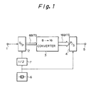
- reference numeral 1 denotes an input terminal which is supplied with digital data to be recorded on a recording medium such as magneto-optical disc
- numeral 2 refers to a serial-parallel converter for converting input data into data of 8 parallel bits
- numeral 3 denotes a data converter.
- the data converter 3 which is made of ROM, PLA and so on, is fed with data bits d1, d2, ..., d8 in the form of 8 bits and outputs channel bits c1, c2, ..., c16 in the form of 16 bits.
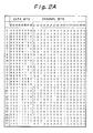
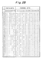
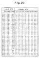
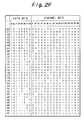
- Tables for converting 8 bits into 16 bits are, for example, as shown in Figs. 2A to 2H.
- the data of 16 parallel bits c1, c2, ..., c16 from the data converter 3 is applied to a parallel-serial converter 4, and recording data of serial bits is obtained at an output terminal 5.
- the recording data is fed to an optical pickup not shown and recorded on a magneto-optical disc.
- the magneto-optical disc is provided with concentrical or vortex tracks. Each track is divided into a predetermined number of sectors and each sector is subdivided into segments. Servo areas are prerecorded on respective segments in an embossing process. Formed in the servo area are an access code coinciding with a lower significant bit of a track address, a clock pit for clock extraction and a wobbling pit for detection of a tracking error. The recording data is recorded in a data area subsequent to the servo area. The access code is used in seeking operation for seeking a target track. When the data is reproduced from the disc, a playback clock synchronizing with a reproduced output of the clock pit in the servo area is formed by the PLL, and the tracking servo is activated by the reproduced output of the wobbling pit.
- a clock generator shown at 6 is provided, and an output signal of the clock generator 6 is supplied to the parallel-serial converter 4.
- the output signal of the clock generator 6 is fed to a 1/2 frequency divider 7, and a clock whose frequency is divided into 1/2 by the 1/2 frequency divider 7 is fed to the serial-parallel converter 2.
- the code conversion tables shown in Figs. 2A to 2H comply with the rule that the data (c1 to c16) obtained by such modulatior never fails to place 2 or more "0"s between "1" and "1", and the rule is complied with also when symbols of 16 bits are coupled.
- Figures 2A to 2H show that last 2 bits c15 and c16 of the channel bits are both "0", and they never fail to comply with the rule that two or more "0"s are present between “1” and “1” even when symbols of 16 bits are coupled.
- Tb indicates intervals of data bits.
- Tw (1/2)
- Tb DR 3/2
- this invention does not necessarily require removal of DC components, and can remove restriction on the maximum length between transition Tmax in a recording/reproducing mode which can form clocks synchronizing with reproduced data, by other means of recorded data. Therefore, the minimum length between transition Tmin and the recording density DR which are parameters other than the maximum length between transition Tmax can be improved.
- required degrees of reducing low frequency components or Tmax usually vary depending on characteristics of transmission paths, contents of transmitted data, and so on.
- a transmission path may have a very bad transmission characteristic as for low frequency components and may require more suppression of low frequency components than that of the EFM.
- Another transmission path may not necessarily require removal of low frequency components or extraction of clocks from modulated data.
- this invention can provide a digital modulator and an associated demodulator circuit having a simple circuit arrangement and readily adaptive to variant characteristics of transmission paths.
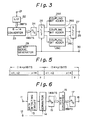
- reference numeral 21 refers to an input terminal supplied with digital data to be recorded on a recording medium such as magneto-optical magnetic disc
- numeral 22 refers to a serial-parallel converter for converting input data into data of 8 parallel bits
- numeral 23 denotes a data converter.
- the data converter 23 which consists of ROM, PLA and others, is supplied with data bits d1, d2, ... and d8 in the form of 8 bits, and supplies channel bits c1, c2, ... and c14 in the form of 14 bits.
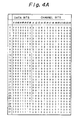
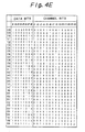
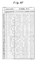
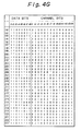
- Tables for converting 8 bits into 14 bits are, for example, as shown in Figs. 4A to 4H which are the same conversion tables as the formerly proposed EFM modulations. More specifically, the code conversion tables shown in Figs. 4A to 4H comply with the rule that two or more "0"s are inserted between "1" and “1", and limit such "0"s between "1" and "1” within 10 pieces in order to shorten Tmax.
- the data of 14 parallel bits c1, c2, ... and c14 from the data converter 23 are fed to the parallel-serial converter 24, from which is obtained a first code signal in the form of serial bits.
- the first code signal is fed to the selector 25.
- the selector 25 has three output terminals which are connected to coupling bit adders 26A, 26B and 26C.
- the coupling bit adders 26A, 26B and 26C are circuits which add coupling bits of p bits as a second code signal to each junction between a 14-bit code signal c1 to c14 and an adjacent such signal formed by the data converter 23.
- These coupling bit adders 26A, 26B and 26C each add coupling bits so as to satisfy the requirement regarding the Tmin in the data converter 23, i.e., the condition that two or more successive "0"s are present between "1" and "1".
- Tb indicates data bit intervals.
- Tw (8/17)
- Tb DR (24/17)
- the coupling bit adder 26A adds 2-bit coupling bits at 14 bits intervals. Therefore, an output signal of the coupling bit adder 26A is made of a 16-bit symbol corresponding to 8-bit data. The output signal of the coupling bit adder 26A is fed to the selector 27.
- the coupling bit adder 26A adds coupling bits (00) to the end of each 14-bit symbol of the EFM conversion tables shown in Figs. 4A to 4H. In this case, 2-bit "0"s may be added to the head of each set of 14 bits obtained from the EFM conversion tables, or 1-bit, "0" may be added to the head and tail, respectively. Further, 2-bit patterns of (10) and (01) may be prepared in addition to (00) to determine coupling bits so as to minimize DSV in the same manner as the coupling bit adder 26B.
- bit patterns (0000), (0001), (0010), (0100), (1000) and (1001) are prepared in the coupling bit adder 26C, and one of the coupling bits is determined, considering which one of the coupling bits should be inserted between successive two 14-bit patterns to minimize DSV. Since more patterns of coupling bits are prepared than those prepared in the coupling bit adder 26B; better suppression of low frequency components can be provided.
- Tb (4/9)Tb
- An output signal of the coupling bit adder 26C is fed to the selector 27.
- the output signal of the coupling bit adder 26B or 26C is suitable for a system to extract clocks from modulated data itself.
- the output signal of the coupling bit adder 26A in the case where a fixed data (00) is suitable for a system having other clock extracting means such as clock bits of a magneto-optical disc. Recording density can be increased most by a system using the coupling bit adder 26A, and it is decreased least by a system using the coupling bit adder 26C. Low frequency components, however, can be reduced most by the system using the coupling bit adder 26C.
- Any one output signal of the coupling bit adders 26A, 26B and 26C selected by the selector 27 is extracted at an output terminal 28.
- a select signal from a select signal generator 29 is supplied to the selectors 25 and 27, and one of output signals of the coupling bit adders 26A, 26B and 26C is selected in response to the select signal.
- the select signal generator 29 generates the select signal in response to a key signal, instructions from a control circuit and so on.
- the modulated data and the select signal taken out at the output terminals 28 and 30, respectively, are converted into recording data by a formating circuit not shown.
- the recording data is fed to an optical pickup or other recording means via a recording amplifier and recorded on a magneto-optical disc or other recording medium.
- Fig. 6 shows an arrangement of digital demodulator associated with the foregoing digital modulator.
- an input terminal shown at 11 is supplied with reproduced data
- an input terminal shown at 12 is supplied with a select signal which is reproduced together with reproduced data.
- the reproduced data is fed to a data detector 13 and its waveform shaping is done.
- An output signal of the data detector 13 is supplied to a separator 14.
- the separator 14 excludes the coupling bits and extracts the first code signal alone.
- the bit number p of the coupling bits is 2 bits, 3 bits or 4 bits as indicated above.
- the select signal indicates the bit number of the coupling bits. Therefore, it is fed to the separator 14.
- the separator 14 separates the first code signal alone in which 14 bits form a symbol.
- An output signal of the separator 14 is supplied to a serial-parallel converter 15 and converted into parallel data of 14 bits.
- the 14-bit data is fed to a data converter 16, which converts the 14-bit data into 8-bit data, in contrast to the modulation process, according to the conversion tables shown in Figs. 4A to 4H.
- the data converter 16 is made of ROM, PLA and so on.
- the 8-bit parallel data from the data converter 16 is fed to a parallel-serial converter 17, and serial output data is obtained at an output terminal 18.
- the data conversion tables are completely identical in three different modulating methods in the foregoing embodiment.
- the invention can be also applied to the case where the conversion rule is identical in most part and different in minor part.
- Kinds of different modulating methods are not limited to three.
- this invention uses a common circuit for converting data excluding coupling bits for different modulating method. Therefore, the circuit having a simple construction, is adaptive to any characteristics of transmission paths, contents of data to be transmitted, and so on.
Landscapes
- Engineering & Computer Science (AREA)
- Signal Processing (AREA)
- Theoretical Computer Science (AREA)
- Signal Processing For Digital Recording And Reproducing (AREA)
Applications Claiming Priority (4)
| Application Number | Priority Date | Filing Date | Title |
|---|---|---|---|
| JP1284401A JP3013366B2 (ja) | 1989-10-31 | 1989-10-31 | ディジタル変調回路及び復調回路 |
| JP284402/89 | 1989-10-31 | ||
| JP1284402A JP3013367B2 (ja) | 1989-10-31 | 1989-10-31 | ディジタル変調方法及び記録方法 |
| JP284401/89 | 1989-10-31 |
Publications (3)
| Publication Number | Publication Date |
|---|---|
| EP0426034A2 true EP0426034A2 (de) | 1991-05-08 |
| EP0426034A3 EP0426034A3 (en) | 1992-01-22 |
| EP0426034B1 EP0426034B1 (de) | 1996-05-08 |
Family
ID=26555456
Family Applications (1)
| Application Number | Title | Priority Date | Filing Date |
|---|---|---|---|
| EP90120597A Expired - Lifetime EP0426034B1 (de) | 1989-10-31 | 1990-10-26 | Schaltung zur digitalen Modulation |
Country Status (3)
| Country | Link |
|---|---|
| US (1) | US5206646A (de) |
| EP (1) | EP0426034B1 (de) |
| DE (1) | DE69026904T2 (de) |
Cited By (1)
| Publication number | Priority date | Publication date | Assignee | Title |
|---|---|---|---|---|
| EP2290962A1 (de) | 1994-09-29 | 2011-03-02 | Sony Corporation | Programminformationsübertragungsverfahren, Programminformationsanzeigeverfahren und Empfangsgerät |
Families Citing this family (8)
| Publication number | Priority date | Publication date | Assignee | Title |
|---|---|---|---|---|
| US5349349A (en) * | 1991-09-30 | 1994-09-20 | Sony Corporation | Modulator circuit for a recording for a digital recording medium |
| US5378174A (en) * | 1993-03-18 | 1995-01-03 | The Whitaker Corporation | Enclosure for variety of terminal blocks |
| KR100231379B1 (ko) * | 1995-04-12 | 1999-11-15 | 니시무로 타이조 | 코드 변환/복호 장치 및 방법 |
| JPH09135172A (ja) * | 1995-11-08 | 1997-05-20 | Sony Corp | 符号変換方法 |
| EP0918398B1 (de) * | 1997-10-24 | 2003-09-17 | Victor Company Of Japan, Ltd. | Signalverarbeitungsvorrichtung |
| EP1303924A2 (de) * | 2000-02-29 | 2003-04-23 | Inari, Inc. | Verfahren und anordnung für stromversorgungsnetz mit hoher datenrate |
| DE60029097T2 (de) * | 2000-08-04 | 2007-06-14 | Stmicroelectronics S.R.L., Agrate Brianza | Pulscodemodulation/Pulsbreitenmodulation-Umsetzer mit Pulsbreitenmodulation-Leistungsverstärker |
| US7949052B1 (en) * | 2003-03-27 | 2011-05-24 | Cisco Technology, Inc. | Method and apparatus to deliver a DVB-ASI compressed video transport stream |
Family Cites Families (9)
| Publication number | Priority date | Publication date | Assignee | Title |
|---|---|---|---|---|
| US3689899A (en) * | 1971-06-07 | 1972-09-05 | Ibm | Run-length-limited variable-length coding with error propagation limitation |
| US4323931A (en) * | 1976-07-14 | 1982-04-06 | Sperry Corporation | Method and apparatus for encoding and recovering binary digital data |
| JPS55141852A (en) * | 1979-04-24 | 1980-11-06 | Sony Corp | Data converting system |
| NL186790C (nl) * | 1980-07-14 | 1991-02-18 | Philips Nv | Werkwijze voor het coderen van een reeks van blokken tweetallige databits in een reeks van blokken van tweetallige kanaalbits, alsmede modulator, demodulator en registratiedrager te gebruiken bij de werkwijze. |
| EP0059224B1 (de) * | 1980-09-05 | 1986-12-03 | Mitsubishi Denki Kabushiki Kaisha | Binäres datenkodier- und -dekodiersystem |
| JPS57132461A (en) * | 1981-02-09 | 1982-08-16 | Sony Corp | Converter for binary data code |
| JPS5846751A (ja) * | 1981-09-11 | 1983-03-18 | Sony Corp | Z値符号変調方法及び記録媒体 |
| US4598326A (en) * | 1983-10-18 | 1986-07-01 | Honeywell Inc. | Digital recording apparatus with disparity reducing encoder |
| DE3587535T2 (de) * | 1984-10-01 | 1994-01-20 | Matsushita Electric Ind Co Ltd | Verfahren und Vorrichtung zur numerischen Datenkodierung. |
-
1990
- 1990-10-26 EP EP90120597A patent/EP0426034B1/de not_active Expired - Lifetime
- 1990-10-26 DE DE69026904T patent/DE69026904T2/de not_active Expired - Fee Related
- 1990-10-26 US US07/603,932 patent/US5206646A/en not_active Expired - Lifetime
Cited By (3)
| Publication number | Priority date | Publication date | Assignee | Title |
|---|---|---|---|---|
| EP2290962A1 (de) | 1994-09-29 | 2011-03-02 | Sony Corporation | Programminformationsübertragungsverfahren, Programminformationsanzeigeverfahren und Empfangsgerät |
| EP2290963A1 (de) | 1994-09-29 | 2011-03-02 | Sony Corporation | Programminformationsübertragungsverfahren, Programminformationsanzeigeverfahren und Empfangsgerät |
| EP2290964A1 (de) | 1994-09-29 | 2011-03-02 | Sony Corporation | Programminformationsanzeigeverfahren und Empfangseinrichtung |
Also Published As
| Publication number | Publication date |
|---|---|
| DE69026904D1 (de) | 1996-06-13 |
| DE69026904T2 (de) | 1997-01-02 |
| EP0426034A3 (en) | 1992-01-22 |
| EP0426034B1 (de) | 1996-05-08 |
| US5206646A (en) | 1993-04-27 |
Similar Documents
| Publication | Publication Date | Title |
|---|---|---|
| JP3227901B2 (ja) | 変調方法及び復調装置 | |
| GB2083322A (en) | Method of coding a sequence of blocks of binary data bits into a sequence of blocks of binary channel bits and arrangement for decoding the data bits coded in accordance with the method | |
| JPH0449304B2 (de) | ||
| US6829306B2 (en) | Method and apparatus of converting a series of data words into a modulated signal | |
| JP3722331B2 (ja) | 変調装置および方法、並びに記録媒体 | |
| US4672362A (en) | Binary data encoding and decoding process | |
| US5633632A (en) | Data conversion method and apparatus imbedding pilot signal into converted data and reducing error propagation between datawords | |
| US5206646A (en) | Digital modulating method | |
| US4549167A (en) | Method of encoding and decoding binary data | |
| US6778105B2 (en) | Method of modulating series of data words into constrained sequence | |
| US6768432B2 (en) | Method of converting a series of m-bit information words into a modulated signal | |
| JPH08235785A (ja) | 記録信号変調装置、記録信号復調装置、記録信号変調方法および記録信号復調方法 | |
| JP3013366B2 (ja) | ディジタル変調回路及び復調回路 | |
| US5812073A (en) | Method and apparatus for generating run-length limited code | |
| JPH0363859B2 (de) | ||
| JP3013367B2 (ja) | ディジタル変調方法及び記録方法 | |
| US20040263362A1 (en) | Coding method and device | |
| KR20040099945A (ko) | 디스크형 기록 매체로의 기록을 위한, 데이터 변조 방법및 그 장치와, 이에 사용되는 싱크 코드 삽입 방법 및 그장치와, 이를 구현하기 위한 프로그램을 기록한 기록 매체 | |
| KR100565079B1 (ko) | 코드 생성 방법, 변조 장치 및 변조 방법 | |
| JP2713011B2 (ja) | 情報変換方法および情報記録装置・情報再生装置 | |
| JPS57183611A (en) | Digital modulating method | |
| AU2001231700A1 (en) | Method of converting a series of M-bit information words into a modulated signal |
Legal Events
| Date | Code | Title | Description |
|---|---|---|---|
| PUAI | Public reference made under article 153(3) epc to a published international application that has entered the european phase |
Free format text: ORIGINAL CODE: 0009012 |
|
| 17P | Request for examination filed |
Effective date: 19901220 |
|
| AK | Designated contracting states |
Kind code of ref document: A2 Designated state(s): DE FR GB NL |
|
| PUAL | Search report despatched |
Free format text: ORIGINAL CODE: 0009013 |
|
| AK | Designated contracting states |
Kind code of ref document: A3 Designated state(s): DE FR GB NL |
|
| 17Q | First examination report despatched |
Effective date: 19950203 |
|
| GRAH | Despatch of communication of intention to grant a patent |
Free format text: ORIGINAL CODE: EPIDOS IGRA |
|
| GRAA | (expected) grant |
Free format text: ORIGINAL CODE: 0009210 |
|
| AK | Designated contracting states |
Kind code of ref document: B1 Designated state(s): DE FR GB NL |
|
| REF | Corresponds to: |
Ref document number: 69026904 Country of ref document: DE Date of ref document: 19960613 |
|
| ET | Fr: translation filed | ||
| PLBE | No opposition filed within time limit |
Free format text: ORIGINAL CODE: 0009261 |
|
| STAA | Information on the status of an ep patent application or granted ep patent |
Free format text: STATUS: NO OPPOSITION FILED WITHIN TIME LIMIT |
|
| 26N | No opposition filed | ||
| REG | Reference to a national code |
Ref country code: GB Ref legal event code: IF02 |
|
| PGFP | Annual fee paid to national office [announced via postgrant information from national office to epo] |
Ref country code: NL Payment date: 20071003 Year of fee payment: 18 Ref country code: DE Payment date: 20071018 Year of fee payment: 18 |
|
| PGFP | Annual fee paid to national office [announced via postgrant information from national office to epo] |
Ref country code: FR Payment date: 20071009 Year of fee payment: 18 Ref country code: GB Payment date: 20071024 Year of fee payment: 18 |
|
| GBPC | Gb: european patent ceased through non-payment of renewal fee |
Effective date: 20081026 |
|
| NLV4 | Nl: lapsed or anulled due to non-payment of the annual fee |
Effective date: 20090501 |
|
| REG | Reference to a national code |
Ref country code: FR Ref legal event code: ST Effective date: 20090630 |
|
| PG25 | Lapsed in a contracting state [announced via postgrant information from national office to epo] |
Ref country code: NL Free format text: LAPSE BECAUSE OF NON-PAYMENT OF DUE FEES Effective date: 20090501 |
|
| PG25 | Lapsed in a contracting state [announced via postgrant information from national office to epo] |
Ref country code: DE Free format text: LAPSE BECAUSE OF NON-PAYMENT OF DUE FEES Effective date: 20090501 |
|
| PG25 | Lapsed in a contracting state [announced via postgrant information from national office to epo] |
Ref country code: FR Free format text: LAPSE BECAUSE OF NON-PAYMENT OF DUE FEES Effective date: 20081031 |
|
| PG25 | Lapsed in a contracting state [announced via postgrant information from national office to epo] |
Ref country code: GB Free format text: LAPSE BECAUSE OF NON-PAYMENT OF DUE FEES Effective date: 20081026 |